Transistors, as power elements of many radio-electronic devices, must perform the following functions for normal operation:
1. Provide control of a given load current with high power gain.
2. Have sufficient (taking into account the given output power and ranges of input and output voltages) power dissipation.
To assemble a radio-electronic device, you can pre-make a DIY KIT kit using the link.
3. Have the maximum permissible collector-emitter voltage, which allows, without the risk of breakdown, to ensure the required voltage drop at the collector-emitter junction at possible values of the input and output voltages.
In some cases, the available transistors do not allow one or more of the conditions described above to be met, then they resort to the help of so-called composite transistors. There are a great many circuits of composite transistors, but there are only three basic circuits.
Why do we need a Darlington circuit?
You must remember that a bipolar transistor is a current controlled element. When a current of known magnitude flows into the base, we expect the collector current to be β times greater, where β is the current gain that couples the base and collector currents together.
Now let's imagine the situation: suppose we want to use a transistor to turn on a motor that draws a current of 5 A. The supply voltage is so low that the use of MOSFETs is not possible, so they remain only bipolar ones. It turns out that transistors capable of conducting such a large current have a β parameter in the range of 40–100.
Divide the collector current by the current gain. The result will be in the range of 50–125 mA. Therefore, to saturate the transistor, it is necessary to provide a base current at least three times higher than the calculated one, that is, about 150–375 mA. However, our microcontroller (like Arduino) can only supply 20mA (safe performance for a single output), which is definitely too low... This is where the Darlington circuit comes in handy.
Circuits for testing transistor timing parameters
Input signal diagram.
Measuring circuit for resistive load.
Mode parameters:
- UCC = 125 V.
- RC = 125 Ohm.
- RB = 47 Ohm.
- D1 diode 1N5820 or similar.
- SCOPE – Tektronics 475 oscilloscope or similar.
- tr, tf ˂ 10 ns; duty cycle ≤ 1%.
Measurement diagram with the parameters of the elements with an inductive load of the transistor.
- Input signal: rectangular pulse with an amplitude of 5 V and the length of the tr and tf fronts no more than 10 ns. Pulse duty cycle 10%.
- The pulse length is selected from the required value of the collector current IC.
- UCC is selected from the required IC value.
- RB is selected from the required value of IB1.
- The MR826 diode is selected for a voltage of 1 kV.
- Limiting voltage UCLAMP = 300 V.
Diagrams of output currents and voltages.
On the image:
- tf CLAMPED – decay time of the current pulse when the voltage is limited at the UCLAMPED level.
- IC(PK) is the maximum achievable current value, based on which the UCC value and input pulse duration are selected.
Calculation formulas: t1 = L × IC(PK) / UCC; t2 = L × IC(PK) / UCLAMP.
Darlington circuit idea
If one transistor can amplify the current, will using two transistors improve our situation? Yes, that's right, it will improve. All we need to do is combine our transistors into a Darlington circuit, this circuit was developed in 1953 by Sidney Darlington.
Approximate connection of two bipolar transistors in a Darlington circuit
When describing the operation of a Darlington circuit, we assume that the collector current is equal to the emitter current (for simplicity, we omit the base current here). We will also take into account that the circuit uses the same type of bipolar transistors. The principle of operation is as follows: the current supplied to the base of T1 flows from its emitter amplified. Let us denote the current gain of this transistor β T1.
T1 flows from the emitter I BT1 · β T1 and directly affects the base of T2. Transistor T2 is amplified by β T2 - multiple. As a result, current I BT1 · β T1 · β T2 flows through the collector T2. Much more of the current flows through T2, so T1's collector current can be considered negligible.
| As a result, the overall current gain of this system is β D = β T1 · β T2. |
Distribution of currents flowing in a Darlington circuit
When transforming the formulas, we made several simplifications. However, they will have little effect on the result (about one percent). The current gain of transistors fluctuates much more (temperature, manufacturer).
| If you have trouble understanding the diagram above, try drawing it on a piece of paper yourself (step by step). |
Advantages of the Darlington circuit
Darlington transistors are used in the same way as single bipolar ones. They can be considered as one transistor with changed parameters. The most important feature of this change is the multiplication of the current gains.
Let's return to the example given at the beginning: combining a power transistor with β = 40 with a smaller value of β, we get a gain of 1600. To turn on a load that consumes 5 A, only 3 mA is required - this is the current that most microcontrollers successfully provide.
Read also: What is a smartphone?
However, it must be remembered that the transistors in this connection are not evenly loaded: most of the current passes through T2. This means that they do not have to be the same type. For example, T1 could be a low power transistor with a large β, making the resulting gain even higher!
Sziklai pair and cascode circuit
Another name for a compound semiconductor triode is a Darlington pair. In addition to her, there is also a couple of Siklai. This is a similar combination of a dyad of basic elements, which differs in that it includes different types of transistors.
As for the cascode circuit, this is also a variant of a composite transistor, in which one semiconductor triode is connected according to a circuit with an OE, and the other according to a circuit with an OB. Such a device is similar to a simple transistor, which is included in a circuit with an OE, but has better frequency characteristics, high input impedance and a large linear range with less distortion of the transmitted signal.
Disadvantages of the Darlington scheme
Unfortunately, that's where the benefits end. The first drawback of this circuit is that the voltage at the emitter base is twice as high. Here we are dealing with a series connection of base-emitter junctions, so the voltages on each of them add up (about 0.7 V when turned on).
| This means that the UBE of the Darlington circuit is approximately 1.4 volts. This should be taken into account when choosing base current limiting resistors. |
However, a much more serious disadvantage is the increased saturation voltage. This issue is best analyzed using a voltage recording diagram.
Voltage distribution in a saturated Darlington transistor
The collector-emitter voltage of a Darlington transistor consists of:
- base-emitter voltage of transistor T2,
- collector-emitter voltage T1.
When the system is saturated, transistor T2 should still be on, that is, its base-emitter voltage is 0.7 V. Due to this, transistor T1 can saturate properly and its U CE drops to an arbitrary level of 0.2 V. After summation These voltage values, it turns out that U CE of transistor T2 is as much as 0.9 V!
| This voltage loss must be taken into account when designing the circuit because it is definitely not a value that can be neglected! |
In our example circuit from the beginning of this article, a single transistor has a big advantage: in a saturated state it will have about 0.2 V (in practice a little more), which, combined with the 5 A current flowing through the collector, will lead to power dissipation about 1 W.
This amount of heat can be easily dissipated using a small radiator, that is, an element that removes heat. It is usually made of aluminum, which is lightweight and conducts heat well. Radiators have different shapes - most often in cross section they resemble a comb, increasing the surface of contact with the flowing air.
Radiator - heat sink element
But let's get back to controlling our engine. If we use Darlington, this power will be wasted, and we will need a much stronger radiator. In addition, the receiver supply voltage will be lower by about 1 V. In the case of circuits powered from a low voltage, such as 3.3 V, this will be a significant reduction.
| 5 W is a lot of power. 5 W, for example, can be consumed by an LED table lamp. |
And also, in a clogged state, the collector-emitter voltage of both transistors is almost the same. This means that when driving the receiver from a power source, for example 60 V, both transistors must withstand this voltage (with a margin).
Modifications (versions) of transistors of the 13003 series
Design - TO-92. Ta = 25°C.
| Type, marking on body | PC, W | UCB, B | UCE, V | IC, A | UCE(sat), V | Time parameters ton / ts / tf µs |
| TS13003HU Marking TSC13003H | 0,5 | 900 | 530 | 1,5 | 1 | — / 4 / 0,7 |
| 3DD13003S1D 3DD13003V1D | 0,8 | 350 | 200 | 1,5 | 0,45 | 1 / 4,5 / 1 |
| 3DD13003ULD | 0,8 | 350 | 200 | 1,8 | 0,4 | 1 / 4,5 / 1 |
| 13003DE | 0,8 | 600 | 400 | 1,3 | 0,22 | 1 / 5 /1 |
| 13003DF/DH | 0,8 | 600 | 400 | 1,5 | 0,3 | 1 / 5 /1 |
| 3DD13003H1D | 0,8 | 600 | 400 | 1,8 | 0,25 | 1 / 5 /1 |
| BU13003D | 0,8 | 700 | 400 | 1,5 | 0,6 | 0,7 / 2,5 /0,9 |
| APT13003LZ Marking 13003LZ-G1 | 0,8 | 700 | 450 | 0,8 | 0,5 | — |
| 3DD13003B | 0,9 | 700 | 400 | 1,5 | 0,8 | — / 4 / 0,7 |
| CS13003 | 0,9 | 700 | 480 | 1 | 0,5 | — |
| 13003DW | 1 | 350 | 200 | 2 | 0,21 | 1 / 4,5 / 1 |
| MJE13003LF1 MJE13003VF1 | 1 | 400 | 200 | 1,2 | 0,8 | — / 4 / 0,6 |
| MJE13003VG1 | 1 | 400 | 200 | 1,5 | 0,6 | — / 3,5 / 0,6 |
| MJE13003VH1 | 1 | 400 | 200 | 2 | 1 | — / 3,5 / 0,6 |
| MJE13003VI1 | 1 | 400 | 200 | 2,5 | 1,3 | — / 3,5 / 0,6 |
| MJE13003VK1 BR3DD13003VK1K Marking BR13003V | 1 | 400 | 200 | 3 | 1,5 | — / 3,5 / 0,6 |
| MJE13003G1/F1 | 1 | 600 | 400 | 0,75 | 0,5 | — / 3,5 / 0,6 |
| MJE13003H1 | 1 | 600 | 400 | 1,2 | 0,8 | — / 3,5 / 0,6 |
| MJE13003DG1 | 1 | 600 | 400 | 1,3 | 0,5 | — / 3,5 / 0,6 |
| MJE13003DI1/I1 | 1 | 600 | 400 | 1,5 | 0,8 | — / 3,5 / 0,6 |
| MJE13003DK1 | 1 | 600 | 400 | 1,75 | 0,5 | — / 4 / 0,5 |
| MJE13003B | 1 | 700 | 400 | 1 | 1 | — / — / 0,3 |
| MJE13003M1 | 1 | 700 | 400 | 1,8 | 0,8 | — / 4 / 0,8 |
| R13003F1 MJE13003E1 | 1 | 700 | 450 | 0,5 (0,45) | 0,5 | — / 4 / 0,6 |
| 13003ADA | 1 | 700 | 450 | 1,5 | 0,18 | — / 4 / 0,7 |
| 13003BS | 1 | 800 | 450 | 2 | 0,8 | 2 / 5 / 2 |
| 13003EDA | 1 | 850 | 500 | 1,3 | 0,2 | 1 / 5 / 1 |
| SBN13003HB | 1 | 850 | 850 (530) | 1 | 1 | 1 / 4 / 0,7 |
| MJE13003T1 MJE13003J1G | 1 | 900 | 530 | 1,5 | 1 | — / 6 / 1,2 |
| MJE13003L1 | 1 | 900 | 530 | 1,5 | 0,8 | — / 5 / 1,2 |
| CSL13003 TSL13003 | 1,1 | 600 | 400 | 1,5 | 1 | 1,1 / 4 / 0,7 |
| SBN13003A1 | 1,1 (1,14) | 700 | 400 | 1,5 | 1 | 0,25 / 1,32 / 0,23 |
| STD13003Q FJN13003 MJE13003A MJE13003D-P MJE13003E KSB13003AR KSB13003A KSB13003ER | 1,1 | 700 | 400 | 1,5 | 1 | 1 / 4 / 0,7 |
| R13003F1 | 1,1 | 700 | 450 | 0,5 (0,45) | 0,5 | — / 4 / 0,6 |
| MJE13003E1 | ||||||
| APT13003SZ Marking 13003SZ-G1 | 1,1 | 700 | 450 | 1,3 | 0,6 | 1 / 3 / 0,5 |
| APT13003DZ APT13003EZ Marking 3003DZ | 1,1 | 700 | 450 | 1,5 | 0,4 | 1 / 3 / 0,4 |
| KSB13003CB KSB13003C | 1,1 | 800 | 450 | 1,5 | 0,5 | 1,1 / 4 / 0,7 |
| APT13003HZ Marking 13003HZ-G1 | 1,1 | 800 | 450 | 1,5 | 0,4 | 1 / 3 / 0,4 |
| KSB13003H | 1,1 | 900 | 530 | 1,5 | 0,8 | 1,1 / 4 / 0,7 |
| 13003DF | 1,25 | 600 | 400 | 1,5 | 0,3 | 1 / 5 / 1 |
| 13003DH | 1,25 | 600 | 400 | 1,8 | 0,3 | 1 / 5 / 1 |
| STX13003 Marking X13003 | 1,5 | 700 | 400 | 1 | 1 | 1 / 4 / 0,7 |
| TS13003CT TS13003BCT Marking TSC13003B | 1,5 | 700 | 400 | 1,5 | 1 | 1 / 4 / 0,7 |
| ST13003H | 1,5 | 900 | 500 | 1,5 | 1 | 1 / 4 / 0,7 |
| TS13003HV | 1,5 | 900 | 530 | 1,5 | 1 | 1,1 / 2 / 0,4 |
| PHE13003A | 2,1 | 700 | 400 | 1 | — | — |
| PHD13003C PHE13003C | 2,1 | 700 | 400 | 1,5 | — | — |
| TS13003MVCT Marking TSC13003H | 5,8 | 800 | 400 | 1,5 | 0,8 | 1 / 4 / 0,6 |
| WBN13003B2D | 15 | 600 | 400 | 1,2 | 0,3 | 1 / 4 / 0,4 |
| WBN13003A1 | 18 | 600 | 400 | 1,2 | 0,8 | — / 4 / 0,7 |
| WBN13003B | 18 | 600 | 400 | 1,5 | 0,5 | 0,2 / 1,5 / 0,15 |
Design of TO-126 (D/F/S). Tc = 25°C.
| Transistor type | PC, W | UCB, B | UCE, V | IC, A | UCE(sat), V | Time parameters ton / ts / tf µs |
| 13003DE | 0,8 | 600 | 400 | 1,3 | 0,22 | 1 / 4 / 1 |
| MJE13003HT | 1,3 | 850 | 500 | 1 | 0,5 | — |
| 3N13003GP BD13003B | 1,5 | 700 | 400 | 1,5 | 0,6 | 1 / 4 / 0,5 |
| MJE13003D-P | 1,5 | 700 | 400 | 1,5 | 1 | 1 / 4 / 0,7 |
| P13003 | 12 | 700 | 400 | 1 | 0,6 | 0,7 / 3,5 / 0,9 |
| H13003H | 12 | 900 | 600 | 1,6 | 0,6 | 1 / 3,0 / 0,8 |
| S13003AD-H | 15 | 800 | 500 | 1,6 | 0,6 | 1 / 3,5 / 0,8 |
| WBR13003B3 | 18 | 600 | 450 | 1 | 0,3 | 0,2 / — / 0,15 |
| J13003 | 18 | 700 | 400 | 1,2 | 0,6 | 0,7 / 4 / 0,9 |
| WBR13003LD | 20 | 350 | 200 | 3 | 0,5 | — / 4 / 0,8 |
| MJE13003LF5 | 20 | 400 | 200 | 1,2 | 0,8 | — / 4 / 0,6 |
| MJE13003VH5 | 20 | 400 | 200 | 2 | 0,5 | — / 3,5 / 0,6 |
| MJE13003VI5 | 20 | 400 | 200 | 2,5 | 0,5 | — / 3,5 / 0,6 |
| MJE13003VK5 | 20 | 400 | 200 | 3 | 0,5 | — / 3,5 / 0,6 |
| MJE13003F6 | 20 | 600 | 400 | 0,5 | 0,5 | — / 4 / 0,6 |
| MJE13003F5 | 20 | 600 | 400 | 0,8 | 0,5 | — / 4 / 0,6 |
| MJE13003BR | 20 | 600 | 400 | 1 | 0,3 | — / 2,4 / 1 |
| WBR13003B2 WBR13003B2D | 20 | 600 | 400 | 1,2 | 0,3 | 0,2 / — / 0,18 |
| WBR13003X | 20 | 600 | 400 | 1,2 | 0,8 | — / 4 / 0,7 |
| WBR13003B1 | 20 | 600 | 400 | 1,2 | 1,6 | 1 / 5 / 1 |
| S13003 | 20 | 600 | 400 | 1,5 | 0,6 | 0,7 / 2,5 / 0,9 |
| WBR13003 | 20 | 600 | 400 | 1,5 | 0,18 | — / 4 / 0,7 |
| 13003 | 20 | 700 | 400 | 1,5 | 0,5 | 1 / 4 / 0,7 |
| 13003D | 20 | 700 | 400 | 1,5 | 1,3 | 1 / 4 / 0,7 |
| KSE13003 | 20 | 700 | 400 | 1,5 | 1 | 1,1 / 4 / 0,7 |
| MJE13003E | 20 | 700 | 400 | 1,5 | 2,5 | 0,5 / 2 / 0,4 |
| P13003D | 20 | 700 | 400 | 1,5 | 0,6 | 0,7 / 2,5 / 0,9 |
| SBR13003BD | 20 | 700 | 400 | 1,5 | 0,2 | 0,2 / 1,5 / 0,15 |
| APT13003SU Marking EU13003S/GU13003S | 20 | 700 | 450 | 1,3 | 0,6 | 1 / 3 / 0,5 |
| 13003ADA | 20 | 700 | 450 | 1,5 | 0,18 | — / 4 / 0,7 |
| APT13003DU Marking GU13003D | 20 | 700 | 450 | 1,5 | 0,4 | 0,7 / 3 / 0,35 |
| APT13003EU Marking EU13003E/GU13003E | 20 | 700 | 465 | 1,5 | 0,29 | 0,3 / 1,8 / 0,28 |
| APT13003HU Marking GU13003H | 20 | 800 | 465 | 1,5 | 0,4 | 0,3 / 1,8 / 0,28 |
| 13003BS | 20 | 800 | 450 | 2 | 0,8 | 2 / 5 / 2 |
| 13003EDA | 20 | 850 | 500 | 1,3 | 0,2 | 1 / 5 / 1 |
| KSC13003H | 20 | 900 | 530 | 1,5 | 1 | 1,1 / 4 / 0,7 |
| SBR13003H | 20 | 900 | 530 | 1,5 | 1 | 0,25 / 1,32 / 0,23 |
| MJE13003HV | 20 | 900 | 530 | 1,5 | 2,5 | 1,1 / 3 / 0,7 |
| S13003DL | 22 | 400 | 200 | 3 | 0,6 | 0,7 / 2,5 / 0,9 |
| 13003A-D | 22 | 700 | 400 | 1,8 | 0,6 | 0,7 / 2,5 / 0,9 |
| 13003A | 22 | 700 | 400 | 1,8 | 0,6 | 0,7 / 2,5 / 0,9 |
| S13003A | 22 | 700 | 400 | 1,8 | 0,6 | 0,7 / 2,5 / 0,9 |
| H13003AH | 22 | 880 | 700 | 2,5 | 0,6 | 0,5 / 3,5 / 0,5 |
| S13003ADL | 25 | 400 | 200 | 3,5 | 0,6 | 1 / 2,5 / 0,9 |
| 13003F BU13003F S13003AD | 25 | 650 | 400 | 2 | 0,6 | 1 / 3,1 / 0,8 |
| SBR13003B1 | 25 | 700 | 400 | 1,5 | 0,5 | 0,2 / 1,5 / 0,15 |
| H13003 | 26 | 650 | 400 | 2 | 0,6 | 0,9 / 3,3 / 0,9 |
| H13003D | 26 | 650 | 400 | 2 | 0,6 | 0,5 / 3,3 / 0,5 |
| H13003ADL | 28 | 400 | 200 | 4 | 0,6 | 0,6 / 2,9 / 0,6 |
| H13003AD | 28 | 700 | 400 | 2,3 | 0,6 | 0,8 / 3,5 / 0,8 |
| H13003DL | 29 | 400 | 200 | 4 | 0,6 | 0,3 / 3 / 0,3 |
| H13003VG5 | 30 | 400 | 200 | 1,5 | 0,6 | — / 4 / 0,6 |
| MJE13003G5/G6 | 30 | 600 | 400 | 0,75 | 0,5 | — / 3,5 / 0,6 |
| NJM13003-1.63 | 30 | 600 | 400 | 1,5 | 0,35 | — / 3 / 0,8 |
| WBR13003 | 30 | 600 | 400 | 1,5 | 0,5 | 0,2 / 1,5 / 0,3 |
| MJE13003BR | 30 | 600 | 400 | 2 | 0,35 | — / 3 / 0,8 |
| MJE13003DG5 | 30 | 700 | 400 | 1,3 | 0,5 | — / 3 / 0,8 |
| SBR13003B | 30 | 700 | 400 | 1,5 | 0,5 | 0,2 / 1,5 / 0,15 |
| TS13003 | 30 | 700 | 400 | 1,5 | 1 | 0,5 / 2 / 0,4 |
| MJE13003HN6 | 30 | 1400 | 800 | 1,5 | 0,6 | — / 6 / 4 |
| 3DD13003U6D | 35 | 350 | 200 | 1,5 | 0,45 | 1 / 4,3 / 1 |
| 3DD13003V6D | 35 | 350 | 200 | 1,8 | 0,4 | 1 / 4,5 / 1 |
| 13003DW | 35 | 350 | 200 | 2 | 0,21 | 1 / 4,5 / 1 |
| 13003C | 35 | 700 | 400 | 2 | — | — |
| WBR13003L2 | 40 | 350 | 200 | 1,5 | 0,8 | — / 3 / 0,8 |
| 3DD13003W6D | 40 | 350 | 200 | 2 | 0,4 | 1 / 4,5 / 1 |
| MJE13003H5/H6 | 40 | 600 | 400 | 1,2 | 0,8 | — / 3,5 / 0,6 |
| 3DD13003E6D | 40 | 600 | 400 | 1,3 | 0,4 | 1/ 4/ 1 |
| MJE13003I6 | 40 | 600 | 400 | 1,5 | 0,8 | — / 3,5 / 0,6 |
| C13003 | 40 | 600 | 400 | 1,5 | 1 | 1 / 4 / 0,7 |
| WBR13003D | 40 | 600 | 400 | 2 | 1,6 | — / 3 / 0,8 |
| CR13003 | 40 | 700 | 400 | 1,5 | 1 | 1 / 4 / 0,7 |
| MJE13003 | 40 | 700 | 400 | 1,5 | 1 | 0,5 / 2 / 0,4 |
| SBR13003A | 40 | 700 | 400 | 1,5 | 0,5 | 0,2 / 1,5 / 0,15 |
| SBR13003D | 40 | 700 | 400 | 1,5 | 1,6 | — / 3 / 0,8 |
| MJE13003DJ5 | 40 | 800 | 480 | 1,5 | 0,8 | — / 3,5 / 0,6 |
| CD13003 CD13003D | 45 | 600 | 400 | 1,5 | 1 | 1,1 / 4 / 0,7 |
| 13003E | 45 | 700 | 400 | 2,5 | — | — |
| MJE13003VN5 | 50 | 400 | 200 | 5 | 0,6 | — / 4 / 0,6 |
| 13003DF 13003DH 3DD13003F6D | 50 | 600 | 400 | 1,5 | 0,3 | 1 / 5 / 1 |
| MJE13003DK5 | 50 | 600 | 400 | 1,75 | 0,9 | — / 4 / 0,8 |
| 3DD13003H6D | 50 | 600 | 400 | 1,8 | 0,25 | 1 / 5 / 1 |
| 3DD13003K6 | 50 | 700 | 400 | 1,8 | — | — |
| 3DD13003I6D 3DD13003I7D | 50 | 700 | 400 | 2 | 0,5 | 1 / 5 / 0,8 |
| 3DD13003N5 | 50 | 700 | 400 | 2 | 0,8 | — / 6 / 0,8 |
| MJE13003DN5 | 50 | 700 | 400 | 2 | 0,6 | — / 6 / 0,8 |
| 3DD13003X1 | 50 | 700 | 400 | 2 | 0,3 | 1 / 4,5 / 2 |
| 3DD13003D | 50 | 700 | 400 | 2,5 | 0,5 | 1 / 5 / 0,8 |
| MJE13003M5/M6 | 50 | 700 | 450 | 1,8 | 0,8 | — / 4 / 0,8 |
| MJE13003HK5 | 50 | 900 | 530 | 1,2 | 0,8 | — / 5 / 1,2 |
| MJE13003L5/L6 | 50 | 900 | 530 | 1,5 | 0,8 | — / 6 / 1,2 |
Design TO-220 (AB/HW/F). Tc = 25°C (unless otherwise stated).
| Type, marking on body | PC, W | UCB, B | UCE, V | IC, A | UCE(sat), V | Time parameters ton / ts / tf µs |
| ST13003 | 1,5 | 600 | 400 | 1,5 | 1 | 1 / 4 / 0,7 |
| SBP13003 | 20 | 700 | 400 | 1,5 | 0,5 | — / 4 / 0,8 |
| 13003B | 28 | 650 | 400 | 2 | 0,6 | 0,5 / 3,3 / 0,5 |
| 13003AD | 30 | 700 | 400 | 2,3 | 0,6 | 0,8 / 3,5 / 0,8 |
| KSE13003T KSH13003H | 30 | 700 | 400 | 1,5 | 0,5 | 1,1 / 4 / 0,7 |
| SBP13003H | 30 | 900 | 530 | 1,5 | 0,5 | 0,2 / 1,32 / 0,23 |
| HMJE13003E | 35 | 700 | 400 | 1,5 | 0,5 | — |
| WBP13003D | 40 | 600 | 400 | 2 | 0,5 | — / 4 / 0,8 |
| MJE13003D | 40 | 700 | 400 | 1,5 | 0,5 | 1 / 4 / 0,7 |
| SBP13003D | 40 | 700 | 400 | 1,5 | 0,5 | — / 4 / 0,8 |
| SBP13003O | 40 | 700 | 400 | 1,5 | 0,5 | — / 4 / 0,3 |
| XW13003-220 | 45 | 600 | 400 | 1,5 | — | — |
| BR3DD13003VK7R Marking BR13003V | 50 | 400 | 200 | 3 | 0,5 | — / 3,5 / 0,6 |
| MJE13003VK7 | 50 | 400 | 200 | 3 | 0,5 | — / 3,5 / 0,6 |
| MJE13003VN7 | 50 | 400 | 200 | 5 | 0,6 | — / 4 / 0,6 |
| MJE13003I7 | 50 | 600 | 400 | 1,5 | 0,8 | — / 3,5 / 0,6 |
| MJE13003K7 MJE13003K8 | 50 | 600 | 400 | 1,5 | 0,9 | — / 4 / 0,8 |
| MJE13003DK7 | 50 | 600 | 400 | 1,75 | 0,9 | — / 4 / 0,8 |
| CDT13003 | 50 | 600 | 400 | 1,8 | 0,5 | 1,1 / 4 / 0,7 |
| MJE13003M7 MJE13003M8 | 50 | 700 | 400 | 1,8 | 0,8 | — / 4 / 0,8 |
| MJE13003N8 | 50 | 700 | 400 | 2 | 0,8 | — / 6 / 0,8 |
| 3DD13003M8D | 60 | 600 | 400 | 1,8 | 0,25 | 1 / 5 / 1 |
| 3DD13003K8 | 60 | 700 | 400 | 1,8 | 0,3 | 1 / 5 / 1 |
| 3DD13003J8D | 60 | 700 | 400 | 2 | 0,5 | 1 / 4 / 1 |
| 3DD13003M8D | 60 | 700 | 400 | 2 | 0,5 | 1 / 4 / 1 |
Design of TO-251. Tc = 25°C (unless otherwise stated).
| Type, marking on body | PC, W | UCB, B | UCE, V | IC, A | UCE(sat), V | Time parameters ton / ts / tf µs |
| MJE13003HT | 1,0 | 850 | 500 | 2 | 0,5 | — |
| MJE13003K3 | 10 | 700 | 450 | 1,5 | 0,9 | — / 4 / 0,8 |
| 13003ADA | 10 | 700 | 450 | 1,5 | 0,18 | — / 4 / 0,7 |
| 13003BS | 10 | 800 | 450 | 2 | 0,8 | 2 / 5 / 2 |
| 13003EDA | 10 | 850 | 500 | 1,3 | 0,2 | 1 / 5 / 1 |
| MJD13003 | 15 | 700 | 400 | 1,5 | 0,5 | 1 / 4 / 0,7 |
| SBU13003BD | 20 | 700 | 400 | 1,5 | 0,6 | 1 / 3 / 0,4 |
| STD13003 | 20 | 700 | 400 | 1,5 | 0,9 | 1 / 4 / 0,7 |
| APT13003DI | 24 | 700 | 450 | 1,5 | 0,3 | 0,7 / 3 / 0,35 |
| ALJ13003 ALJ13003-251 | 25 | 600 | 400 | 1,2 | 0,8 | — / 6 / 1 |
| KSU13003E KSU13003ER | 25 | 700 | 400 | 1,5 | 0,5 | 1,1 / 4 / 0,7 |
| MJE13003K | 25 | 700 | 400 | 1,5 | 0,5 | 1 / 4 / 0,7 |
| MJE13003P | 25 | 700 | 400 | 1,5 | 0,5 | 1 / 4 / 0,7 |
| KSU13003H KSU13003HR | 25 | 900 | 530 | 2 | 0,8 | 1,1 / 4 / 0,7 |
| 3DD13003U3D | 30 | 350 | 200 | 1,8 | 0,4 | 1 / 4,5 / 1 |
| MJE13003VK3 | 30 | 400 | 200 | 3 | 1,5 | — / 3,5 / 0,6 |
| 3DD13003F3D | 30 | 600 | 400 | 1,5 | 0,3 | 1 / 4,5 / 1 |
| MJE13003DK3 | 30 | 700 | 400 | 1,75 | 0,9 | — / 4 / 0,8 |
| MJE13003DI3 | 30 | 800 | 480 | 1,5 | 0,8 | — / 3,5 / 0,6 |
| 13003DW | 35 | 350 | 200 | 2 | 0,21 | 1 / 4,5 / 1 |
| 3DD13003W3D | 35 | 350 | 200 | 2 | 0,4 | 1 / 4,5 / 1 |
| 3DD13003H3D | 35 | 600 | 400 | 1,8 | 0,25 | 1 / 5 / 1 |
| HI13003 | 40 | 700 | 400 | 1,5 | 0,5 | — |
| MJE13003M3 | 40 | 700 | 400 | 1,8 | 0,8 | — / 4 / 0,8 |
| MJE13003H3 | 40 | 700 | 450 | 1,2 | 0,8 | — / 3,5 / 0,6 |
| MJE13003L3 | 40 | 900 | 530 | 1,5 | 0,8 | — / 6 / 1,2 |
| 13003DH | 50 | 600 | 400 | 1,8 | 0,3 | 1 / 5 / 1 |
| MJE13003I | 50 | 600 | 400 | 1,5 | 0,8 | — / 3,5 / 0,6 |
Design of TO-252. Tc = 25°C (unless otherwise stated).
| Type, marking on body | PC, W | UCB, B | UCE, V | IC, A | UCE(sat), V | Time parameters ton / ts / tf µs |
| MJE13003HT | 1,0 | 850 | 500 | 2 | 0,5 | — |
| CZD13003 | 1,25 | 700 | 400 | 1,5 | 1 | — / 2,5 / 0,5 |
| DXT13003DK Marking 13003D | 3,9 | 700 | 450 | 1,5 | 0,3 | 0,35 / 2,3 / 0,21 |
| DXT13003EK Marking 13003E | 3,9 | 700 | 460 | 1,5 | 0,3 | 0,43 / 1,64 / 0,28 |
| WBD13003D | 10 | 600 | 400 | 2 | 0,5 | — / 4 / 0,8 |
| HJ13003 | 15 | 700 | 400 | 1,5 | — | — |
| STD13003D | 15 | 700 | 400 | 1,5 | 0,5 | 1,1 / 4 / 0,7 |
| CJD13003 | 15 | 700 | 400 | 1,5 | 0,5 | 1,1 / 4 / 0,7 |
| STD13003 | 20 | 700 | 400 | 1,5 | 0,5 | 1 / 4 / 0,7 |
| KSD13003E KSD13003ER | 25 | 700 | 400 | 1,5 | 0,5 | 1,1 / 4 / 0,7 |
| MJE13003K | 25 | 700 | 400 | 1,5 | 0,5 | 1 / 4 / 0,7 |
| MJE13003P | 25 | 700 | 400 | 1,5 | 0,5 | 1 / 4 / 0,7 |
| KSH13003 KSH13003I | 40 | 700 | 400 | 1,5 | 0,5 | 1,1 / 4 / 0,7 |
| MJE13003K4 | 50 | 600 | 400 | 1,5 | 0,9 | — / 4 / 0,8 |
Design versions TO-826, SOT23, SOT223, SOT89, LSTM. Tc = 25°C (unless otherwise stated).
| PC, W | UCB, B | UCE, V | IC, A | UCE(sat), V | Time parameters ton / ts / tf µs | Type, marking on body |
| 0,5 | 350 | 200 | 1,5 | 0,45 | 1 / 3,5 / 1 | 3DD13003SUD Housing SOT23, TO89S |
| 0,5 | 350 | 200 | 1,5 | 0,45 | 1 / 4 / 1 | 3DD13003SUD Housing SOT23, TO89S |
| 0,5 | 700 | 400 | 1,5 | 0,6 | — / 4 / 0,5 | 3DD13003/A/C/E/F SOT89 housing |
| 0,9 | 600 | 400 | 1,5 | 1 | 0,4 / 1,4 / 0,2 | TTC13003L, LSTM Marking 13003L |
| 1,0 | 600 | 400 | 0,5 | 0,5 | — / 4 / 0,6 | MJE13003FT, SOT89 Marking H03F |
| 1,25 | 700 | 450 | 1,5 | 1 | 1 / 4 / 0,7 | PZT13003 |
| 3,0 | 700 | 450 | 1,3 | 0,4 | 0,7 / 3 / 0,35 | DXT13003DG Marking 13003D |
| 20 | 600 | 400 | 1,5 | 0,6 | 0,7 / 2,5 / 0,9 | S13003, TO826 |
| 20 | 700 | 400 | 0,5 | 1,2 | — / 2,5 / 0,18 | ST13003N, SOT32 Marking 13003N |
| 20 | 700 | 400 | 0,5 | 1,2 | — / 2,5 / 0,18 | ST13003DN, SOT32 Marking 13003DN |
| 22 | 700 | 400 | 1,8 | 0,6 | 0,7 / 2,5 / 0,9 | S13003A |
| 25 | 650 | 400 | 2 | 0,6 | 12 / 3,1 / 0,8 | S13003AD |
| 26 | 650 | 400 | 2 | 0,6 | 0,5 / 3,3 / 0,5 | H13003D |
| 28 | 700 | 400 | 2,3 | 0,6 | 0,8 / 3,5 / 0,8 | H13003AD |
| 40 | 700 | 400 | 1,5 | 1 | 1 / 4 / 0,7 | ST13003D-K, SOT32 Marking 13003D |
| 40 | 700 | 400 | 1,5 | 1 | 1 / 4 / 0,7 | ST13003K, SOT32 Marking 13003 |
| 40 | 700 | 400 | 1,5 | 1 | 1 / 4 / 0,7 | STK13003, SOT82 |
Note: the table data is obtained from the datasheet of the manufacturing companies.
Darlington circuit in practice
It's time to test the properties of the Darlington circuit in practice. Of course, according to the previous diagram, such a configuration can be built “manually” using two transistors. However, this circuit is so popular that manufacturers also sell ready-made Darlington transistors that have this dual connection and look like a regular single transistor.
In our experiment, we will use the MPSA29 (β>10000) transistor , which is an off-the-shelf Darlington transistor. Let's compare its performance with the previously reviewed BC546 (β = 200–450). This time, we'll build two versions of a "graphite paper potentiometer" in which one of the paths through which current flows will be drawn in pencil on a piece of paper!
Read also: What is soldering?
To complete this exercise you will need:
- Resistor 1 × 10 kOhm,
- Resistor 1 × 1 kOhm,
- 1 × LED (choose your favorite color),
- 1 × BC546 transistor,
- 1 × MPSA29 transistor,
- 1 × pencil,
- 1 × sheet of paper,
- 4 × AA batteries, 1 × slot for 4 AA batteries,
- 1 × development board,
- set of connecting wires.
| When doing the exercises, note that the BC546 and MPSA29 transistors have different pin positions (see below for details)! |
First make the potentiometer by yourself. On a piece of paper, draw a thick line with a pencil, several centimeters long. Draw the pencil along the line several times to make sure it is clear (one stroke is not enough because the carbon footprint on the sheet will not be continuous). As you probably know, graphite conducts electricity, but has a fairly high resistance. By drawing a line, you have made a resistor with a resistance of hundreds of kilo-ohms per centimeter. You can check this with help. multimeter.
Using a multimeter, you can measure the resistance of a line drawn with a pencil
Now we need to place a chip on the breadboard that will use our graphite resistor . For now we will use the well known BC546 transistor. However, you should immediately pay attention to the different pinout arrangement of the MPSA29!
Comparison of BC546 and MPSA29 transistor pinouts
We will use the graphite line as a "potentiometer" to regulate the current flowing through the base. Simply press the wires onto a piece of paper. The greater the distance between the conductors, the greater the resistance between them. A 10 kOhm resistor is used to protect the transistor from fire if these wires are accidentally short-circuited.
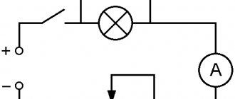
Circuit diagram for BC546 gain testing
In practice, the whole scheme might look like this:
| Assembling the circuit on a breadboard | Scheme with BC546 in practice |
It's time to check how the circuit behaves at different resistances . When performing this exercise, do not touch the “potentiometer” wires with your fingers - the skin resistance is relatively low, which will disrupt the progress of this experiment.
| Resistance is low - LED is on | Resistance is high - LED does not light up |
The longer the path between the ends of the wires, the higher the resistance and less current flows into the base. At what length of the track does the LED stop lighting? Record your result, turn off the power and replace the transistor with an MPSA29. However, remember that this transistor has a different emitter and collector!
Circuit diagram for MPSA29 amplification testing
In practice, the whole scheme might look like this:
| Circuit on breadboard | Example with MPSA29 |
After assembling the circuit, turn on the power, and again press the ends of the wires to the track on the sheet. Now the distance between the wires on which the LED lights up should be much greater. This is all thanks to the properties of the new transistor, which has a much higher beta gain.
| Resistance is low - LED is on | Resistance is high - LED is still on |
Darlington transistors are slow!
The Darlington circuit has a certain phenomenon that makes it very difficult to operate at high frequencies. Switching it, and especially turning it off, takes a lot of time (for electronics).
Let's look at the circuit diagram again. When the power is turned on, the potential of the T1 base is raised (for example, by a microcontroller), thereby introducing current into it. This transistor very quickly goes from a blocked state to an active state, in which it amplifies this current and supplies it to the base of T2, which is also turned on very efficiently. Everything happens pretty quickly.
Read also: What is 3G technology?
| Let's assume that this transistor is used to turn on a high-power receiver, such as a motor, that requires it to be heavily saturated. |
An approximate diagram of connecting two bipolar transistors to a Darlington circuit.
Now turn off the Darlington transistor. The base potential of T1 is pulled to ground by a resistor. The charge carriers accumulated in this base must flow away from it through this resistor. Since T1 was “really” saturated, there were quite a lot of such carriers there.
During this time, T2 was still conductive, although it should no longer be so. Assuming that the carriers have left the T1 base, the question is: where should the carriers leave the T2 base? The only way out is the base, but only a clogged transistor is connected to it... We can only wait until these carriers spontaneously “dissipate” and the transistor finally stops conducting.
The following illustrations demonstrate this phenomenon (the current values, of course, do not reflect the real ones - they serve only to illustrate the scale and the fact of the current flow; RL and the motor symbol symbolize some element that is powered by the transistor, for example a motor).
| Both transistors are non-conducting | Current flow through the base activates both transistors |
In the off state the situation is as follows:
| Charge accumulated after turning off the current | The captured charge slowly dissipates |
Thus, two events influence the switching off of the Darlington transistor:
- removal of saturation and clogging T1,
- waiting until transistor T2 stops conducting.
The first problem can be somehow solved by using, for example, appropriate circuits to speed up the switching of transistors. However, there is a problem with the latter, because the media must provide a flow from the base to the emitter.
Electronics has come up with a way to partially solve this problem. This method involves adding a resistor between the base and emitter of T2. Thanks to this, charge carriers find a way out of the base. One disadvantage is the reduction in current gain because this resistor "steals" current from the emitter of T1.
Such modified Darlington transistors are commercially available as single units or as integrated circuits with many components inside. A good example is the popular ULN2003 microcircuit , which includes as many as 7 such systems.
Popular chip ULN2003
This chip also includes resistors that limit the base current of T1 (2.7 kOhm) and speed up the turn-off of T1. The use of such integrated blocks is convenient because it saves space on the board; the input of this circuit is connected directly to the output of the microcontroller.
Internal diagram of ULN2003
The principle of construction and operation of inverter welding machines
Influence of operating frequency on transformer dimensions
A transformer is a necessary element of any welding source.
It reduces the network voltage to the arc voltage level, and also provides galvanic isolation of the network and the welding circuit. It is known that the dimensions of a transformer are determined by its operating frequency, as well as the quality of the magnetic core material. Note.
As the frequency decreases, the dimensions of the transformer increase, and as the frequency increases, they decrease.
Transformers of classical sources operate at a relatively low network frequency. Therefore, the weight and dimensions of these sources were mainly determined by the mass and volume of the welding transformer.
Recently, various high-quality magnetic materials have been developed that make it possible to somewhat improve the weight and size parameters of transformers and welding sources. However, a significant improvement in these parameters can only be achieved by increasing the operating frequency of the transformers. Since the frequency of the mains voltage is standard and cannot be changed, it is possible to increase the operating frequency of the transformer using a special electronic converter.
Block diagram of inverter welding source
A simplified block diagram of an inverter welding source (IWS) is shown in Fig. 1 . Let's look at the diagram. The mains voltage is rectified and smoothed, and then supplied to the electronic converter. It converts direct voltage into high frequency alternating voltage. High-frequency alternating voltage is transformed using a small-sized high-frequency transformer, then rectified and fed into the welding circuit.
Rice. 1
Transformer types
The operation of the electronic converter is closely related to the magnetization reversal cycles of the transformer. Since the ferromagnetic material of the transformer core has nonlinearity and is saturated, the induction in the transformer core can only grow to a certain maximum value Vm.
After reaching this value, the core must be demagnetized to zero or remagnetized in the opposite direction to the value – Bm. Energy can be transmitted through a transformer:
- in the magnetization cycle;
- in the magnetization reversal cycle;
- in both cycles.
Definition.
Converters that provide energy transfer in one cycle of magnetization reversal of the transformer are called single-cycle .
Accordingly, converters that provide energy transfer in both magnetization reversal cycles of the transformer are called push-pull .
Single-ended forward converter
Advantages of single-ended converters. Single-cycle converters are most widely used in cheap and low-power inverter welding sources designed to operate from a single-phase network. Under conditions of sharply variable load, such as the welding arc, single-cycle converters compare favorably with various push-pull converters:
- they do not require balancing;
- they are not susceptible to such a disease as through currents.
Therefore, to control this converter, a simpler control circuit is required compared to what would be required for a push-pull converter.
Classification of single-cycle converters. According to the method of transferring energy to the load, single-cycle converters are divided into two groups: forward and flyback ( Fig. 2 ). In forward converters, energy is transferred to the load at the moment of the closed state, and in flyback converters - at the moment of the open state of the key transistor VT. In this case, in a flyback converter, energy is stored in the inductance of the transformer T during the closed state of the switch and the switch current has the shape of a triangle with a rising edge and a steep cutoff.
Rice. 2
Note.
When choosing the type of ISI converter between forward and flyback, preference is given to a forward single-ended converter.
Indeed, despite its great complexity, a forward converter, unlike a flyback converter, has a high power density . This is explained by the fact that in a flyback converter a triangular current flows through the key transistor, and in a forward converter, a rectangular current flows. Consequently, at the same maximum switch current, the average current value of a forward converter is twice as high.
The main advantages of a flyback converter are:
- lack of a choke in the rectifier;
- possibility of group stabilization of several voltages.
These advantages provide an advantage to flyback converters in various low-power applications, such as power supplies for various household television and radio equipment; as well as service power supplies for the control circuits of the welding sources themselves.
Transformer of a single-transistor forward converter (SFC) , shown in Fig. 2, b , has a special demagnetizing winding III. This winding serves to demagnetize the core of the transformer T, which is magnetized during the closed state of the transistor VT.
At this time, the voltage on winding III is applied to diode VD3 in blocking polarity. Due to this, the demagnetizing winding does not have any influence on the magnetization process.
After turning off the transistor VT:
- the voltage on winding III changes its polarity;
- diode VD3 is unlocked;
- the energy accumulated in the transformer T returns to the primary power source Up.
Note.
However, in practice, due to insufficient coupling between the transformer windings, part of the magnetizing energy is not returned to the primary source. This energy is typically dissipated in the VT transistor and snubber circuits (not shown in Figure 2 ), degrading the overall efficiency and reliability of the converter.
Oblique bridge. This disadvantage is absent in a two-transistor forward converter (FFC) , which is often called an “oblique bridge” ( Fig. 3, a ). In this converter (due to the introduction of an additional transistor and diode), the primary winding of the transformer is used as a demagnetizing winding. Since this winding is completely connected to itself, the problems of incomplete return of magnetization energy are completely eliminated.
Rice. 3
Let us consider in more detail the processes occurring at the moment of magnetization reversal of the transformer core.
A common feature of all single-ended converters is that their transformers operate in conditions with one-way magnetization.
Magnetic induction B (in a transformer with one-way magnetization) can only vary within the range from maximum Bm to residual Br, describing a partial hysteresis loop.
When transistors VT1, VT2 of the converter are open, the energy of the power source Up is transferred to the load through transformer T. In this case, the transformer core is magnetized in the forward direction (section a-b in Fig. 3 , b).
When transistors VT1, VT2 are locked, the current in the load is maintained by the energy stored in the inductor L. In this case, the current is closed through the diode VD0. At this moment, under the influence of the EMF of winding I, the diodes VD1, VD2 open, and the demagnetization current of the transformer core flows through them in the opposite direction (section b-a in Fig. 3, b ).
The change in induction ∆B in the core occurs practically from Bm to Br and is significantly less than the value ∆B = 2·Bm possible for a push-pull converter. Some increase in ∆B can be obtained by introducing a non-magnetic gap into the core. If the core has a non-magnetic gap δ, then the residual induction becomes less than Br . If there is a non-magnetic gap in the core, the new value of the residual induction can be found at the intersection point of a straight line drawn from the origin at an angle Ѳ to the magnetization reversal curve (point B1 in Fig. 3, b ):
tgѲ= µ0 lc/δ,
where µ0 – magnetic permeability;
lc – length of the average magnetic field line of the magnetic core, m;
δ – length of non-magnetic gap, m.
Definition.
Magnetic permeability is the ratio of induction B to tension H for a vacuum (also valid for a non-magnetic air gap) and is a physical constant, numerically equal to µ0=4π·10-7H/m.
The value tgѲ can be considered as the conductivity of the non-magnetic gap reduced to the length of the core. Thus, introducing a non-magnetic gap is equivalent to introducing a negative magnetic field strength:
Н1 = -В1/ tgѲ.
Push-pull bridge converter
Advantages of push-pull converters. Push-pull converters contain more elements and require more complex control algorithms. However, these converters provide lower input current ripple and greater output power and efficiency from the same discrete key component power.
Scheme of a push-pull bridge converter. In Fig. 4, a shows a diagram of a push-pull bridge converter. If we compare this converter with single-ended converters, it is closest to a two-transistor forward converter ( Fig. 3 ). A push-pull converter is easily converted into it if you remove a pair of transistors and a pair of diodes located diagonally (VT1, VT4, VD2, VD3 or VT2, VT3, VD1, VD4).
Rice. 4
Thus, a push-pull bridge converter is a combination of two single-cycle converters operating alternately. In this case, energy is transferred to the load during the entire period of operation of the converter, and the induction in the transformer core can vary from -Bm to +Bm.
As in the DPP, diodes VD1-VD4 serve to return the energy accumulated in the leakage inductance Ls of the transformer T to the primary power source Up. MOSFET internal diodes can be used as these diodes.
Operating principle. Let us consider in more detail the processes occurring at the moment of magnetization reversal of the transformer core.
Note.
A common feature of push-pull converters is that their transformers operate in conditions with symmetrical magnetization reversal.
Magnetic induction B, in the core of a transformer with symmetrical magnetization reversal, can vary from negative -Bm to positive +Bm maximum induction.
In each half-cycle of the DMP operation, two keys located diagonally are open. During pause, all transistors of the converter are usually closed, although there are control modes when some transistors of the converter remain open during pause.
Let's focus on the control mode, according to which all DMP transistors are closed during a pause.
When transistors VT1, VT4 of the converter are open, the energy of the power source Up is transferred to the load through transformer T. In this case, the transformer core is magnetized in the conventional reverse direction (section b-a in Fig. 4, b ).
During a pause, when transistors VT1, VT4 are closed, the current in the load is maintained by the energy stored in the inductor L. In this case, the current is closed through the diode VD7. At this moment, one of the secondary windings (IIa or IIb) of transformer T is short-circuited through an open diode VD7 and one of the rectifier diodes (VD5 or VD6). As a result of this, the induction in the transformer core remains virtually unchanged.
After the pause is completed, transistors VT2, VT3 of the converter open, and the energy of the power source Up is transferred to the load through transformer T.
In this case, the transformer core is magnetized in the conventional forward direction (section a-b in Fig. 4 ). During a pause, when transistors VT2, VT3 are closed, the current in the load is maintained by the energy stored in the inductor L. In this case, the current is closed through the diode VD7. At this moment, the induction in the transformer core remains virtually unchanged and is fixed at the achieved positive level.
Note.
Due to the fixation of inductions in pauses, the core of the transformer T is capable of reversing magnetization only when the diagonally located transistors are open.
In order to avoid one-sided saturation under these conditions, it is necessary to ensure equal open time of the transistors, as well as symmetry of the power circuit of the converter.