Elements of electrical circuits in all cases, except for a branch, are necessarily present in the set. In practice, you can imagine a circuit diagram in the form of a passive and active two-terminal network.
The grounding and grounding circuit is closed with the help of soil. Otherwise, no current will flow in the circuit.
Electronic elements used in key circuits can be divided into two classes according to their key properties: - elements whose key properties are ensured by setting their operating mode; - elements whose key properties are determined by the very principle of their operation. READING ELECTRICAL DIAGRAMS WITH A TRANSISTOR - PART 3
Otherwise, current will not flow in the circuit. Basic elements during calculations for electrical circuits They are used in complex structures to check what and how will work: Branch.
Nominal mode This mode is necessary to create the technical properties of the entire circuit and individual components. Conclusion So, we have examined electrical circuits, elements of electrical circuits and practical features of interaction with them.
In order for there to be current in a circuit, it must be closed, i.e. Electrical Circuit Diagram Questions What is the purpose of a current source in an electrical circuit?
Taking into account the reactive parameters of the device makes the dynamic equivalent circuit suitable for the analysis of fast processes, in particular for the analysis of processes that arise when a nonlinear circuit is affected by the pulse front. Exercise 23 We have already found out that to use electricity we need things such as a current source, conductors, devices, etc.
Electrical circuits (part 1)
1.1. Switches on bipolar transistors
Table of contents
1. Keys on bipolar transistors……………………………………………………………………………………. 2
1.1.General information…………………………………………………………………………………………. 2
a) Ideal key…………………………………………………………………………………………. 2
b) Real key………………………………………………………………………………………….. 2
c) Transistor switch circuits………………………………………………………………………………………. 3
1.2.Model of a bipolar transistor………………………………………………………………………………….. 3
1.3.Operating mode of bipolar npn transistor…………………………………………………. 4
1.Active mode:…………………………………………………………………………………. 4
2.In cut-off mode:………………………………………………………………………………….. 4
2.a) In deep cut-off mode:………………………………………………………………. 4
2.b) Cut-off limit with active mode:………………………………………………………………. 5
3.In saturation mode:………………………………………………………………………………5
3.a) Saturation limit with active mode:………………………………………….. 5
4.Inverse mode……………………………………………………………………………….. 5
1.4.Transistor switch with OE……………………………………………………………………………………………….. 6
2. Residual parameters of the key on the BT………………………………………………………………………………… 9
2.1. Residual parameters of a closed transistor…………………………………………………………………… 9
2.2. Residual parameters of the saturated transistor……………………………………………. 12
3. Composite transistor switch………………………………………………………………………………… 15
3.1.???…………………………………………………………………………………………………………… 15
a) If transistor VT1 is locked, then…………………………………………………………. 17
b) If the transistor is saturated, then……………………………………………………………… 17
3.2.Multi-emitter transistor in switching mode…………………………………………. 19
a) Apply low voltage to any input……………………………………………………… 20
Electromagnetic relay
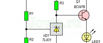
A relay is an electromagnet that controls a group of contacts. An analogy can be drawn with a conventional push-button switch. Only in the case of a relay, the force is taken not from the hand, but from the magnetic field that is located around the excitation coil. The contacts can switch a very large load - it all depends on the type of electromagnetic relay. These devices have become very widespread in automotive technology - with their help, all powerful consumers of electricity are turned on.
This allows you to divide all the electrical equipment of the car into a power part and a control part. The current consumption of the relay excitation winding is very small. And the power contacts are coated with precious or semi-precious metals, which eliminates the possibility of an arc. Transistor switch circuits for 12 volts can be used instead of relays. At the same time, the functionality of the device improves - the switching on is silent, the contacts do not click.
2.2. Bipolar transistor model
Used to obtain the static current-voltage characteristics of the transistor. Based on an equivalent circuit (nonlinear).
The equivalent circuit and Ebers-Moll equations describe the static mode of an idealized transistor and are obtained under the following assumptions:
1) the volumetric resistance values of the base, emitter and collector are negligible;
;
— transfer coefficient.
2) the effect of modulation of the base width when the voltage at the base-collector junction changes is not taken into account (the efficiency of the emitter does not depend on the current);
3) the injection current density is low (the degree of base doping remains constant and low).
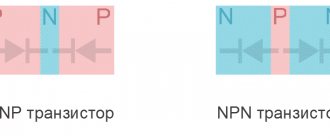
2.3. Operating mode of bipolar npn transistor
In any circuit, regardless of whether it operates in static or dynamic mode, the transistor at any given time operates in one of the following modes: active, cutoff, saturation, inverse.
Active mode:
The emitter junction is forward biased, the collector junction is reverse biased. Potential npn
BT:
| Rice. 1.3.a: ??? | ,; |
In cutoff mode:
The emitter and collector junctions are reverse biased. Potential cut-off criterion:,.
2.1) In deep cut-off mode:
if the voltage blocking the emitter and collector junctions significantly exceeds the temperature potential.
Potential criterion:
,;
,;
2.2) Cut-off limit with active mode:
if the collector junction is locked and the voltage at the emitter junction is “0”.
,;
In saturation mode:
both junctions are forward biased (double injection mode).
,;
3.1) Saturation limit with active mode:
if the emitter junction is forward biased and the voltage at the collector junction is zero:
,;
Inverse mode
called the mode when the emitter junction is biased in the opposite direction, and the collector junction is forward biased. In this case, the collector works as an emitter, i.e., it injects carriers into the base, and the emitter performs the functions of a collector.
,.
In transistor switches, the transistor can operate in all of the specified modes. If the BT operates in cut-off mode or in active mode at very low collector currents, then it is an open switch. If it operates in saturation mode or active mode at high collector currents, it acts as a closed switch. During the transition from one state to another, the BT operates in active mode.
Scheme of the simplest electrical circuit
So, the simplest version of the electrical circuit is shown in Figure 3.
Figure 3. Diagram of a simple electrical circuit
What parts does it consist of?
- Current source
- Current receiver
- Closing device
- Connecting wires
In this case, the current source is a galvanic cell or battery, the receiver is a light bulb, and the closing device is a key. All these elements are connected to each other by wires.
3.1. Residual parameters of a closed transistor
a) When the value of the blocking voltage at the emitter junction changes, that is, when the cutoff depth () changes, the base current does not change and remains equal. This equality is called the current cutoff criterion.
b) Both in the deep cutoff mode and at the cutoff boundary, the emitter current is .
The equivalent circuit of the key in cut-off mode can be represented as:
| Rice. 2.1.a: Equivalent circuit of a key in cut-off mode |
Switch output voltage
c) From the diagram it is clear that the voltage applied to the emitter, control junction depends on the residual base current;
.
In its turn .
To maintain the cutoff mode when changing from and resistances, it is necessary to fulfill the following condition:
.
Otherwise, despite the negative polarity of the control signal, the transistor will switch to active mode.
d) In transistor switches, it is necessary to use transistors with low reverse transition currents.
Note:
Integrated circuits do not use negative control signals to turn off transistors because digital circuits are single-supply powered. The open state of the key does not correspond to the cut-off mode, but to the active mode at low collector current. This has a beneficial effect on reducing the duration of transient processes.
|
The transistor turn-off threshold is a conditional value. The more open, the more can be selected. Usually accepted.
Electronic signature or digital signature?
Previously, the bypass contained the abbreviation EDS - electronic digital signature. But after Federal Law No. 63 came into force, this name was shortened to ES, electronic signature. It is for electronic signature that an electronic key is used. According to the legislation of the Russian Federation, an electronic signature is understood as the equivalent of a signature, which is placed “by hand” and has similar legal force. Electronic signature allows individuals to remotely (via the Internet) sign documents with government, financial, medical, educational and other institutions. Legal entities can use it to participate in electronic auctions, conduct electronic document management (EDF), submit reports to the tax office, etc.
3.2. Residual parameters of a saturated transistor.
| Rice. 2.2.a Designation of voltages at the terminals of the transistor | ; |
a) The smallest of the residual stresses is . Therefore, it is desirable to use a switch such that the residual voltage is , that is, the preferred circuit is a switch with an OE.
b) Dependence of residual stresses on the degree of saturation
|
are the voltages at open junctions, they increase with increasing.
decreases with increase.
c) In real transistors, residual voltages depend on the voltage drops across the volumetric resistances of the layers. At high currents, the voltage drops increase.
Since the “K” layer has a large resistance and length??? the current through it is high, a hidden “n+” sublayer is introduced into the design of the epitaxial-planar transistor.
|
d) The weak dependence of interelectrode voltages on “N” allows us to present the equivalent circuit of a transistor in saturation mode in the following form:
Rice. 2.2.d: Equivalent circuit of a transistor in saturation mode |
;
.
Since residual voltages are small compared to the power supply voltage, they can often be neglected. The simplified equivalent circuit takes the form:
| Rice. 2.2.d: Transistor-equipotential point |
Required Electrical Circuit Parts
The first thing that must be present in an electrical circuit is a current source .
It will create an electric field and maintain it, an electric current will arise. We can use his energy.
How? For this we need a consumer or receiver of electrical energy . This is the name for all the electrical appliances that we use, from simple light bulbs and flashlights to computers, electric motors, and various household appliances.
The current source and its consumer must be connected to each other by wires . Through them, the current from the source will reach the consumer.
4.1. ???
If the load of the OE key is a sufficiently large capacity, then the key has low performance.
Let's assume that the transistor in the key circuit turns off instantly.
Rice. 3.1.a: Key diagram after switching (previously it was saturated) |
The output voltage is the voltage across the capacitor.
The previously discharged capacity begins to charge with current.
The duration of the front is determined by the charging time of the capacitance, that is. Since it is several kOhms, the duration of the falling edge turns out to be unacceptably long.
| For example: ; . Then . |
To improve the parameters of the key, it is built according to the structural diagram:
Rice. 3.1.b: Key structure diagram |
In this circuit, there is a low-resistance circuit for charging.
The principle of operation of a composite key is as follows.
When a positive pulse arrives at the input, the OE switch closes and the OK switch opens. The load capacity is quickly discharged through a saturated OE switch. The output voltage is close to zero.
At the end of the positive pulse, the OE key opens and the OK key closes. Now the load capacity is charged through the saturated OK switch. Since the saturation current of the transistor is high, the capacitance is charged quickly.
Rice. 3.1.c: Schematic diagram of a composite key |
A star key is assembled on transistor VT1, which represents a combination of OE and OK keys. The signal at the collector has a polarity opposite to the polarity of the input signal, that is, the collector circuit VT1 acts as an inverter. The emitter circuit VT1 does not invert the signal.
VT2 - OK key;
VT3 - OE key.
1) If transistor VT1 is locked, then
.
Since, transistor VT3 is also locked.
The voltage at the collector VT1 is:
and close to the supply voltage.
Therefore, transistor VT2 is open and the load capacitance in steady state is charged to voltage
,
where , is the voltage drop across the emitter junction of the open transistor VT2 and across the open diode VD1.
2) If the transistor is saturated, then
and transistor VT3 is also in saturation mode. In this case, VT2 must be locked. To do this, it is necessary that the voltage at its base be less than or equal to the voltage at the emitter or
From the last relationship it is clear that in the absence of a diode in the circuit, the condition for turning off transistor VT2 is not satisfied.
In this state of the key, the capacitance is discharged through the saturated transistor VT3 and the voltage across it (low level).
During the transition process, due to the delay in turning off the transistors, some transistors (both VT2 and VT3) are open for some time. This results in an inrush of current drawn by the key from the power supply. To limit this current, a small resistance is introduced into the collector circuit of transistor VT2
Often, transistor VT2 with diode VD is replaced with a composite transistor VT2′, VT2".
Rice. 3.1.d: Composite transistor VT2′, VT2" |
The principle of operation of the circuit does not change. The function of the bias diode VD here is performed by the emitter junction of transistor VT2.”
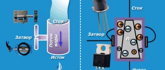
How a field-effect transistor works: 6 types - brief information
The classification shown in the picture below, where their types are structured, will help us deal with a specific field grass and understand its structure.
JFET and MOSFET have different structure. In JFET, the gate (Gate) is directly built into the cross section of the channel and works as a control pn junction.
For mosfet:
- there is an additional fourth pin connected internally to the housing. It is not used when connecting to external circuits;
- The gate output region is separated by a layer of silicon dioxide (dielectric) from the channel semiconductor. It works as a plate capacitively coupled capacitor. Due to this modification, it is called an “insulated gate” or MOS transistor.
MIS stands for metal-dielectric-semiconductor and MOS stands for metal-oxide-semiconductor. The difference between them for a novice electrician is not significant, practically absent.
In the diagrams, mosfet and jifet are designated in different ways. MOSFET is drawn with:
- the fourth pin, which is not connected anywhere;
- a shutter separated from the main channel.
Mosfets are manufactured with different substrates (channels), which can be depleted or enriched in major charge carriers.
I will not describe and describe in more detail the differences between each type of these semiconductors for a novice electrician: there is not much point.
Below are just typical schedules of their work. They will give a general idea of behavior, and you will need to take specific data from the datasheet - technical documentation.
The amount of current flowing through the drain depends on the applied voltage between gate and source, as well as the ambient temperature.
The output drain current characteristics depend on the magnitude of the applied voltage between drain-source and gate-source.
This is how a MOS transistor with a built-in channel works. The current slope increases with increasing voltage Usi, Uzi.
And here are the characteristics of transistors with an induced channel.
Before any check of each transistor, it is necessary to clarify its technical capabilities according to the factory documentation.
Such graphical images and dependencies of electrical engineering processes, due to their clarity, have better information content.
6 features of electronic devices using MOSFETs
Recently, we are increasingly working with mosfet-type field devices with a channel of any conductivity.
Let us briefly analyze such a scheme and its properties.
Point No. 1: which shoulder to place the load on?
When a semiconductor junction is fully open, a very small resistance of tens or hundreds of milliOhms (Ropen) is created between drain and source, which creates a low voltage drop across
and in this section (In·Ropen), where In is the value of the load current.
The voltage potential applied to the gate may not be sufficient to fully open the semiconductor. Therefore, the load is turned on higher on the drain side in an n-type field switch, and on the source side in a p-type field switch when the circuit is powered from a single source.
If the device uses additional voltage sources, then this requirement is not necessary.
Point No. 2: tricks for connecting a field worker to microcontrollers
For reliable operation of the MOSFET, it is necessary to apply a threshold voltage value between its gate and source (gate-source), which is indicated in the datasheet. It is usually around 10 volts. Still, digital devices work up to five: their power supply is not enough, you will need to add a level.
You can solve the problem in one of three ways:
- a key with bipolar transistors supplies the necessary power to the gate;
- connect a special driver (chip) to generate a control signal. They are designed for both the upper and lower shoulder to accommodate the load. Moreover, the high-side driver often uses a circuit to increase the output voltage;
- use a specialized low-level field operator (logic level). However, acquiring it can be problematic.
Point No. 3: how to avoid the influence of electrical interference
The appearance of any interference potential at the output of a transistor often leads to its unauthorized switching and disruption of electronic operating algorithms.
Therefore, the gate is always “pulled” to power or ground through a certain resistance, even when connected through a microcontroller. It should not be left in a free state, accessible to the penetration of extraneous interference.
We recommend reading: How to make a radio-controlled airplane at home
Point No. 4: combating surge current when turned on
The natural presence of capacitance at the gate pin leads to a “current surge” each time the transistor is turned on. This can lead to damage to the semiconductor junction.
The problem is solved by introducing a resistor of sufficient value into the gate circuit. However, its value must be selected taking into account the increase in the key opening time.
Feature No. 5: inrush current protection when disconnecting inductive loads
A protective high-speed TVS diode, connected in parallel between the source and drain, reliably shunts the pulses created by disconnecting inductive loads.
When operating at high frequencies in bridge or half-bridge circuits of switching power supplies or induction heaters of hobs, a Schottky diode is connected counter-currently to the drain output, blocking the parasitic diode, because it increases the closing time, which can damage the semiconductor.
Point No. 6: additional MOSFET protection
Safe operation of a high-speed high-frequency switch in the switching mode of powerful inductive loads is ensured by its connection to snubber circuits. They:
- aperiodic currents created by transient processes close on themselves;
- reduce heating of semiconductors;
- protect the field switch from unauthorized opening during a rapid increase in voltage between drain and source.
4.2. Multi-emitter transistor in switching mode
A multi-emitter transistor (MET) is designed to perform logical functions in a TTL element.
Rice. 3.2.a: Physical structure of a multi-emitter transistor??? |
The MET has several emitters (four in the above design), located in such a way that direct interaction between them through the disconnecting sections of the base is excluded. MET is several transistor structures that have a common collector.
Rice. 3.2.b: Connection circuit for a multi-emitter transistor |