Hello dear readers of the site. In the first part of the article, we figured out what a semiconductor is and how current arises in it. Today we will continue the topic we started and talk about the operating principle of semiconductor diodes .
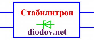
Diode
is a semiconductor device with one
p-n
junction, which has two terminals (anode and cathode), and is designed for rectification, detection, stabilization, modulation, limitation and conversion of electrical signals.
According to their functional purpose, diodes are divided into rectifier, universal, pulse, microwave diodes, zener diodes, varicaps, switching, tunnel diodes, etc.
Theoretically, we know that a diode passes current in one direction and not in the other. But how and in what way he does this is not known and understood by many.
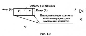
Schematically, a diode can be represented as a crystal consisting of two semiconductors (regions). One region of the crystal has conductivity p
-type, and the other with
n
-type conductivity.
There are holes in the picture
electrons that predominate in the
p
-type region are conventionally depicted as red circles, and
electrons
that predominate in
the n
-type region are shown in blue.
These two areas are the diode's electrodes anode
and
cathode
:
Anode - positive electrode
diode in which the main charge carriers are
holes
.
Cathode - negative electrode
diode in which the main charge carriers are
electrons
.
Contact contacts are applied to the outer surfaces of the areas.
metal layers to which the wire
leads
of the diode electrodes are soldered. Such a device can only be in one of two states:
1. Open
– when it conducts current well;
2. Closed
- when it conducts current poorly.
Direct connection of the diode. Direct current.
If you connect a constant voltage source to the diode electrodes: to the anode terminal “ plus
" and the cathode terminal is "
minus
", then the diode will be in
the open
state and a current will flow through it, the magnitude of which will depend on the applied voltage and the properties of the diode.
With this polarity of connection, electrons from the region n
-type electrons will move towards the holes into the
p
-type region, and holes from the
p
-type region will move towards the electrons into the
n
-type region.
At the interface between the regions, called an electron-hole or pn junction , they will meet, where their mutual absorption or recombination
.
For example. Major charge carriers in the n
-type electrons, overcoming
the p-n
junction, enter the
p
-type hole region, in which they become
minority
.
Having become minority electrons, they will be absorbed by majority
carriers in the hole region -
holes
.
In the same way, holes entering the n
-type electronic region become
minority
charge carriers in this region, and will also be absorbed by
the majority
carriers -
electrons
.
Diode pin connected to negative
The pole of a constant voltage source will
give up
n
region , replenishing the decrease in electrons in this region.
And the contact connected to the positive
pole of the voltage source is able
to accept
the same number of electrons
from the
p p
-type region is restored.
Thus, the conductivity the p-n
junction will become
large
and the current resistance will be
small
, which means that a current will flow through the diode, called
diode current Ipr
.
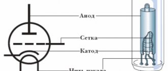
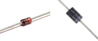
Device
The following is installed in a housing made in the form of a vacuum cylinder made of ceramic, glass or metal:
- crystal;
- anode;
- cathode;
- heater.
Crystals are made from silicon or germanium. The anode (plus) and cathode (minus) are cylindrical in shape and placed inside the cylinder. A heater is a filament inside the cathode that heats up when an electric current is applied, heating it. After reaching a certain temperature level, the active layer on the cathode generates the electrons necessary for operation.
Reverse connection of the diode. Reverse current.
Let's change the polarity of the constant voltage source - the diode will be closed
condition.
In this case, electrons in the region n
-type will move towards
the positive
pole of the power source, moving away from
the p-n
junction, and holes in the
p
-type region will also move away from
the p-n
junction, moving towards
the negative
pole of the power source.
As a result, the boundary of the regions will seem to expand, which creates a zone depleted of holes and electrons, which will provide great
resistance to the current.
But, since in each of the regions of the diode there are minor
charge carriers, then a small exchange of electrons and holes between the regions will still occur.
Therefore, a current many times less than the forward current will flow through the diode, and such a current is called the reverse current of the diode ( Irev
).
As a rule, in practice, the reverse current p-n
junction is neglected, and from this we conclude that
the p-n
junction has only
one-way conductivity
.
Video
Coffee capsules Nescafe Dolce Gusto Café Au Lait, 16 pcs.
435 ₽ More details
Coffee capsule Nescafe Dolce Gusto Latte Macchiato with caramel flavor, 3 packs of 16 capsules each
1305 ₽ More details
Monitors 144 Hz
Forward and reverse diode voltage.
The voltage at which the diode opens and direct current flows through it is called forward
(Upr), and the voltage of reverse polarity, at which the diode closes and reverse current flows through it, is called
reverse
(Urev).
At forward voltage ( Upr
) the resistance of the diode does not exceed several tens of ohms, but with reverse voltage (
Urev
) the resistance increases to several tens, hundreds and even thousands of kiloohms. This is not difficult to verify if you measure the reverse resistance of the diode with an ohmmeter.
Resistance pn
diode transition value is not constant and depends on the forward voltage (
Upr
), which is supplied to the diode.
The greater
this voltage, the
less
the p-n
has , the
greater
the forward current
Ipr
flows through the diode.
In the closed state drops
, therefore, the reverse current passing through it
is small
, and the resistance of
the p-n
junction
is high
.
For example. If you connect a diode to an alternating current circuit, it will open at positive
half-cycles at the anode, freely passing
forward current
(Ipr), and close at
negative
half-cycles at the anode, almost without passing current in the opposite direction -
reverse current
(Irev).
These properties of diodes are used to convert alternating current into direct current
, and such diodes are called
rectifying
.
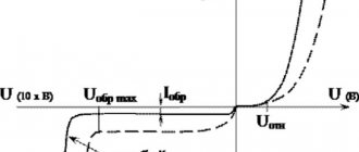
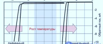
Current-voltage characteristic of a semiconductor diode.
Dependence of the current passing through pn
the transition, depending on the magnitude and polarity of the voltage applied to it, is depicted in the form of a curve called
the current-voltage characteristic of the diode .
The graph below shows such a curve. Vertical _
The axis in the upper part indicates the values of the forward current (
Ipr
), and in the lower part - the reverse current (
Irev
).
Along the horizontal
axis on the right side the values of the forward voltage
Upr
, and on the left side the values of the reverse voltage (
Urev
) are indicated.
The current-voltage characteristic consists of two branches: direct branch
, in the upper right part, corresponds to the forward (pass) current through the diode, and
the reverse branch
, in the lower left part, corresponding to the reverse (closed) current through the diode.
Direct branch
goes steeply upward, pressing against
the vertical
axis, and characterizes the rapid increase in forward current through the diode with increasing forward voltage.
The reverse branch
runs almost parallel to
the horizontal
axis and characterizes a slow increase in the reverse current.
The steeper the forward branch is to the vertical axis and the closer the reverse branch is to the horizontal, the better the rectifying properties of the diode. The presence of a small reverse current is a disadvantage of diodes
.
From the current-voltage characteristic curve it is clear that the forward current of the diode ( Ipr
) is hundreds of times greater than the reverse current (
Irev
).
As the forward voltage increases through pn
The transition current initially increases slowly, and then a section of rapid current growth begins.
This is explained by the fact that a germanium
diode opens and begins to conduct current at a forward voltage of 0.1 - 0.2V, and
a silicon diode
at 0.5 - 0.6V.
For example. At forward voltage Upr
= 0.5V forward current
Ipr
is equal to 50mA (point “
a
” on the graph), and already at a voltage
Upr
= 1V the current increases to 150mA (point “
b
” on the graph).
But such an increase in current leads to heating of the semiconductor molecule. And if the amount of heat generated is greater than that removed from the crystal naturally, or using special cooling devices ( radiators
), then irreversible changes can occur in the conductor molecule, up to the destruction of the crystal lattice.
Therefore, the forward current the p-n
junction is limited to a level that prevents overheating of the semiconductor structure. To do this, use a limiting resistor connected in series with the diode.
For semiconductor diodes, the forward voltage Upr is
at all values of operating currents does not exceed: for
germanium
- 1V;
for silicon
- 1.5V.
With an increase in reverse voltage ( Urev
) applied to
the pn
junction, the current increases slightly, as evidenced by the reverse branch of the current-voltage characteristic.
For example. Let's take a diode with the parameters: Urev max
= 100V,
Irev max
= 0.5 mA, where:
Uar max
– maximum constant reverse voltage, V;
Irev max
– maximum reverse current, µA.
With a gradual increase in the reverse voltage to a value of 100V, one can see how the reverse current increases slightly (point “ at
" on the chart).
But with a further increase in voltage, above the maximum for which the pn
breakdown
occurs .
Designation of radio components on electrical circuits
The designation on the diagrams of radio elements appears in the form of graphic figures. For example, a resistor is depicted as an elongated rectangle with the letter “R” and a serial number next to it. “R15” means that the resistor in the circuit is the 15th in a row. The amount of power dissipated by the resistance is immediately prescribed.
Understanding electrical measuring instruments
Particular attention should be paid to the designation on the microcircuits. For example, you can consider the KR155LAZ microcircuit. The first letter "K" means a wide range of applications. If there is an “E”, then this is an export version. The second letter “P” determines the material and type of case. In this case it is plastic. A unit is a type of part, in the example a semiconductor chip. 55 – serial number of the series. The following letters express the AND-NOT logic.
Where to start reading diagrams
You need to start by reading circuit diagrams. For more effective learning, you need to combine the study of theory with practice. You must understand all symbols on the board. There is a lot of information on the Internet for this. It is a good idea to have reference material on hand in book format. In parallel with mastering the theory, you need to learn how to solder simple circuits.
How are radioelements connected in a circuit?
Boards are used to connect radio components. To make contact tracks, a special solution is used to etch copper foil on the dielectric layer of the printed circuit board. Excess foil is removed, leaving only the necessary tracks. The leads of the parts are soldered to their edges.
Additional Information. Lithium batteries, when heated by a soldering iron, can swell and collapse. To prevent this from happening, spot welding is used.
Letter designation of radioelements in the circuit
To decipher the letter designations of parts in the diagram, you need to use special tables approved by GOST. The first letter means the device, the second and third letters specify the specific type of radio component. For example, F stands for arrester or fuse. The full letters FV let you know that this is a fuse.
Graphic designation of radioelements in the circuit
The graphics of the circuits include a conventional two-dimensional designation of radioelements accepted throughout the world. For example, a resistor is a rectangle, a transistor is a circle in which the lines show the direction of the current, a choke is a stretched spring, etc.
A novice radio amateur should have a table of images of radio components at hand. Below are examples of tables of graphic symbols for radio components.
Table of graphic designations of radioelements on the diagram
table 2
Table 3
Table 4
For beginning radio amateurs, it is important to stock up on reference literature where you can find information about the purpose of a particular radio component and its characteristics. You can learn how to make your own printed circuit boards and how to solder circuits correctly using video lessons online.
Electrical breakdown.
Electrical breakdown occurs as a result of exposure to a strong electric field
in
p-n
junction.
Such a breakdown is reversible
, that is, it does not damage the junction, and when the reverse voltage is reduced, the properties of the diode are preserved.
For example. Zener diodes
- diodes designed to stabilize voltage - operate in this mode
Tunnel breakdown.
Tunnel breakdown occurs as a result of the phenomenon of the tunnel effect
, which manifests itself in the fact that with a strong electric field strength acting in
p-n
junction
of small thickness
, some electrons penetrate (leak) through the transition from the
p
the n
region without
changing
their energy.
Thin p-n
junctions are possible only with a high concentration
of impurities
in the semiconductor molecule.
Depending on the power and purpose of the diode, the thickness of the electron-hole junction can range from 100 nm
(nanometers) to
1 micron
(micrometer).
A tunnel breakdown is characterized by a sharp increase in reverse current
with a slight
reverse voltage
- usually a few volts.
Tunnel diodes
operate based on this effect .
Due to their properties, tunnel diodes are used in amplifiers, generators of sinusoidal relaxation oscillations and switching devices at frequencies of up to hundreds and thousands of megahertz.
Avalanche breakdown.
Avalanche breakdown is that, under the influence of a strong electric field, minority
Charge carriers under the influence of
heat
in
a pn
junction are accelerated so much that they are able to
knock out
one of its valence electrons from an atom and
throw
it into the conduction band, thereby forming an
electron-hole
.
The resulting charge carriers will also begin to accelerate and collide with other atoms, forming the following electron-hole pairs. The process takes on an avalanche-like character, which leads to a sharp increase
in reverse current at a practically
constant
voltage.
Diodes that use the avalanche breakdown effect are used in powerful rectifier units
, used in the metallurgical and chemical industries, railway transport and other electrical products in which a reverse voltage higher than permissible may occur.
LED polarity: how to determine plus and minus
When using LEDs in creating various circuits, they must be installed correctly. Soldering in most cases does not create problems; determining the polarity is a little more difficult if you do not have experience working with testing equipment.
How to determine polarity with a multimeter tester
The easiest way to check the LED is with a multimeter. When connecting the pins in the “dialing” mode to the electrodes, you can get 2 results: the LED lights up and displays a number on the screen depending on the color of the radiation, or shows a very large number. With the first option, we can conclude that the light source is working and connected to the multimeter correctly (plus to plus, minus to minus).
The second method of using a multimeter is to switch to resistance testing. If the red probe touches the plus, the black probe touches the minus, a value in the range of 1600–1800 appears on the screen.
Attention! If the LED is broken (passes voltage in two directions), the number “1” appears on the screen. If there is a break, a very large resistance value appears on the screen, regardless of the location of the probes.
If the multimeter has a PNP compartment, the E (emitter - “+”) and C (collector – “-”) compartments are required to determine the polarity of the LED. The light source glows if the cathode is inserted into “C” and the anode into “E”.
If an NPN multimeter compartment is used, the LED will light if the legs are swapped.
By appearance
In the production of LEDs, different housings are used. DIP elements with a cylindrical body of various diameters are widely used. There are many surface mount SMDs being manufactured. Ultra-bright light sources differ in the size of their housings and crystals. An experienced radio amateur determines the cathode and anode by external signs.
For DIP elements:
- longer anode leg;
- the silhouette in the flask is smaller at the anode, the shape of the cathode resembles a flag;
- a source with a power of more than 1 W has a “+” marking on the anode leg.
Attention! If the DIP LED has already been installed in some device and soldered, the dimensions of the legs may change. Plus and minus are determined by the size of the crystal in the flask or by testing with a multimeter.
For SMD LEDs:
- the cathode is indicated by a cut on the body;
- the heat sink on the back of the case is located closer to the anode;
- The “P” pictogram is facing the anode with the top shelf, the top of the “T” pictogram is facing the cathode.