I came across DES-1228 equipment and decided to study the internals in terms of the devices’ power supplies. The photo shows two power supplies from the same equipment, just different modifications.
The upper one is earlier, IES1228ME. A1G
Power supply with INPUT characteristics: 100-240V
50/60Hz 1.2A OUTPUT: 12V = 3.33A
The lower one is later, IES1228ME. A2G
Power supply with INPUT characteristics: 100-240V
50/60Hz 1.2A OUTPUT: 12V = 3.33A
Power supply DES-1228. (SU40-6120333-T) Version 3.33A
Internals of the DES-1228 switch. There are plenty of places for the power supply
Let's see what is written. Earlier version IES1228ME. A1G
Hardware version A1, firmware version 1.00.B04. And a characteristic inscription with a description.
Power supply with INPUT characteristics: 100-240V
50/60Hz 1.2A OUTPUT: 12V = 3.33A
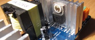
The block itself looks solid, yet it is designed for a current of up to 3.3A (compared to its subsequent brother at 2A) two plates with cooling of a field-effect transistor and a dual diode.
The right side is high voltage (input), the left is low voltage (output). PWM on nL01 chip. I couldn't find a description for this little thing.
I studied and redrew the power supply diagram. (I probably could have missed something). Red indicates elements that should be in the diagram, but they are not.
In this version: - on the side of the SMD components - 5 elements are missing (these are resistors and capacitors that are not sealed) - on the side of the remaining components, the inductor L1 at the input is missing, it is replaced by ordinary jumpers (cheaper design) - three components are not soldered (capacitor and pair of filter Y-capacitors CY2,CY3)
Power supply DES-1228. (SU25-3120200-T) Version 2A
There is the same amount of space inside. The power supplies are interchangeable, the mounting is accordingly the same.
Later version, IES1228ME. A2G
Let's see what is written.
Version higher than IES1228ME. A2G
Hardware version A2, firmware version 1.00.B06.
The characteristic inscription is missing. Simplification number 1. Save on paint)
Power supply with INPUT characteristics: 100-240V
50/60Hz 1.0A OUTPUT: 12V = 2A
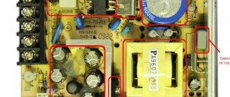
The block looks less solid. Cooling is much less. The capacitor in the high voltage circuit is smaller. The transformer is smaller. Simplification number 2. Save on output current
The right side is high voltage (input), the left is low voltage (output). PWM on a JbP3 chip. I couldn't find a description for this little thing.
I spent some time studying again and a power supply diagram appeared. (perhaps I didn’t take something into account)
Below are two diagrams of both blocks. Elements that are not present in one block are crossed out in red.
Comparison: - the purpose of the shunt circuit of a resistor and diode in the gate circuit of field-effect transistor Q1 (R27, D22) (block 2A) is not clear - in block 2A a resistor R7 97k appears on the 3rd pin of the PWM. — in block 3.3A there is a connection between the common winding of transformer T1 and the 4th pin of the PWM through resistor R3, R6 (750k). in block 2A this connection is absent - the design of block 2A has been simplified, the output inductor L has been eliminated (not provided structurally). And capacitor C6 is missing - otherwise the circuits are identical (the ratings may just be slightly different).
Raising the output voltage of the power supply
Mail1977 suggested and helped. Shouldn't we increase the voltage of the power supply in order to power a larger number of LEDs in one chain? Say, to power 6 LEDs with a voltage drop of 3.2V each, you will need to increase the voltage to 19.5V (3.2 x 6 = 19.2V). We have 1W LEDs with a voltage drop of 3.2V to 3.4V. Therefore, the voltage limit is from 19.2V to 20.4V.
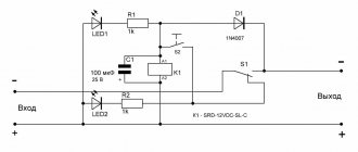
The power supply is built on a “controlled zener diode” TL431.
For those who want to look deeper and see the insides, there is an article “Reverse engineering TL431” habrahabr.ru/post/257387/
In the diagram, a divider consisting of resistors R10 (3.9k) and R13 (1k) is connected to the controlled input. If instead of R10 (highlighted in blue in the diagram)
connect a tuning resistor with a nominal value of 10k Ohm, setting it to 3.9k and turn it smoothly, then the output voltage will change. As the resistance increases, the output voltage will increase. But no more than what is indicated on the output capacitors (25V). I couldn’t raise it above 21-22V. Theoretically, if you replace the capacitors from 25V to 50V, you can try to increase the voltage further.
Similarly, if we decrease the resistance, then the output voltage will decrease. We set the desired voltage with the trimmer and then solder the SMD resistor with a more suitable value. For a more accurate selection, you can combine the values of two series-connected resistors.
I selected resistors experimentally. Instead of R10 in 3k9 I soldered 6.8k + 510 Ohm (it turned out 7.3k). For 3W LEDs, the voltage drop is in the range of 3.2 - 3.8V per LED. This means the total output voltage for 6 LEDs is (20.4 - 22.8V). I chose 3.5V for one LED, and 21V for the circuit.
If we stabilize the voltage, then the current in the circuit will be constant. I set the current for a 3W LED to 640 - 700mA (something from this limit, I don’t know for sure now, but it is constant)
Conclusion: - device power supplies are being improved in the direction of simplifying costs - it is possible to increase the output voltage of the power supply in a simple way
The most interesting
The earlier power supply is the one that could not be raised above 17V at 3.3A, then as the resistance in the TL431 arm increases, the lamps begin to blink and the output voltage jumps... In general, the SU40-6120333-T block (OUTPUT: 12V = 3.33A) can be used for voltage not higher than 17V...
I came across DES-1228 equipment and decided to study the internals in terms of the devices’ power supplies. The photo shows two power supplies from the same equipment, just different modifications.
The upper one is earlier, IES1228ME. A1G
Power supply with INPUT characteristics: 100-240V
50/60Hz 1.2A OUTPUT: 12V = 3.33A
The lower one is later, IES1228ME. A2G
Power supply with INPUT characteristics: 100-240V
50/60Hz 1.2A OUTPUT: 12V = 3.33A
Power supply DES-1228. (SU40-6120333-T) Version 3.33A
Internals of the DES-1228 switch. There are plenty of places for the power supply
Let's see what is written. Earlier version IES1228ME. A1G
Hardware version A1, firmware version 1.00.B04. And a characteristic inscription with a description.
Power supply with INPUT characteristics: 100-240V
50/60Hz 1.2A OUTPUT: 12V = 3.33A
The block itself looks solid, yet it is designed for a current of up to 3.3A (compared to its subsequent brother at 2A) two plates with cooling of a field-effect transistor and a dual diode.
The right side is high voltage (input), the left is low voltage (output). PWM on nL01 chip. I couldn't find a description for this little thing.
I studied and redrew the power supply diagram. (I probably could have missed something). Red indicates elements that should be in the diagram, but they are not.
In this version: - on the side of the SMD components - 5 elements are missing (these are resistors and capacitors that are not sealed) - on the side of the remaining components, the inductor L1 at the input is missing, it is replaced by ordinary jumpers (cheaper design) - three components are not soldered (capacitor and pair of filter Y-capacitors CY2,CY3)
Power supply DES-1228. (SU25-3120200-T) Version 2A
There is the same amount of space inside. The power supplies are interchangeable, the mounting is accordingly the same.
Later version, IES1228ME. A2G
Let's see what is written.
Version higher than IES1228ME. A2G
Hardware version A2, firmware version 1.00.B06.
The characteristic inscription is missing. Simplification number 1. Save on paint)
Power supply with INPUT characteristics: 100-240V
50/60Hz 1.0A OUTPUT: 12V = 2A
The block looks less solid. Cooling is much less. The capacitor in the high voltage circuit is smaller. The transformer is smaller. Simplification number 2. Save on output current
The right side is high voltage (input), the left is low voltage (output). PWM on a JbP3 chip. I couldn't find a description for this little thing.
I spent some time studying again and a power supply diagram appeared. (perhaps I didn’t take something into account)
Below are two diagrams of both blocks. Elements that are not present in one block are crossed out in red.
Comparison: - the purpose of the shunt circuit of a resistor and diode in the gate circuit of field-effect transistor Q1 (R27, D22) (block 2A) is not clear - in block 2A a resistor R7 97k appears on the 3rd pin of the PWM. — in block 3.3A there is a connection between the common winding of transformer T1 and the 4th pin of the PWM through resistor R3, R6 (750k). in block 2A this connection is absent - the design of block 2A has been simplified, the output inductor L has been eliminated (not provided structurally). And capacitor C6 is missing - otherwise the circuits are identical (the ratings may just be slightly different).
Raising the output voltage of the power supply
Mail1977 suggested and helped. Shouldn't we increase the voltage of the power supply in order to power a larger number of LEDs in one chain? Say, to power 6 LEDs with a voltage drop of 3.2V each, you will need to increase the voltage to 19.5V (3.2 x 6 = 19.2V). We have 1W LEDs with a voltage drop of 3.2V to 3.4V. Therefore, the voltage limit is from 19.2V to 20.4V.
The power supply is built on a “controlled zener diode” TL431.
For those who want to look deeper and see the insides, there is an article “Reverse engineering TL431” habrahabr.ru/post/257387/
In the diagram, a divider consisting of resistors R10 (3.9k) and R13 (1k) is connected to the controlled input. If instead of R10 (highlighted in blue in the diagram)
connect a tuning resistor with a nominal value of 10k Ohm, setting it to 3.9k and turn it smoothly, then the output voltage will change. As the resistance increases, the output voltage will increase. But no more than what is indicated on the output capacitors (25V). I couldn’t raise it above 21-22V. Theoretically, if you replace the capacitors from 25V to 50V, you can try to increase the voltage further.
Similarly, if we decrease the resistance, then the output voltage will decrease. We set the desired voltage with the trimmer and then solder the SMD resistor with a more suitable value. For a more accurate selection, you can combine the values of two series-connected resistors.
I selected resistors experimentally. Instead of R10 in 3k9 I soldered 6.8k + 510 Ohm (it turned out 7.3k). For 3W LEDs, the voltage drop is in the range of 3.2 - 3.8V per LED. This means the total output voltage for 6 LEDs is (20.4 - 22.8V). I chose 3.5V for one LED, and 21V for the circuit.
If we stabilize the voltage, then the current in the circuit will be constant. I set the current for a 3W LED to 640 - 700mA (something from this limit, I don’t know for sure now, but it is constant)
Conclusion: - device power supplies are being improved in the direction of simplifying costs - it is possible to increase the output voltage of the power supply in a simple way
The most interesting
The earlier power supply is the one that could not be raised above 17V at 3.3A, then as the resistance in the TL431 arm increases, the lamps begin to blink and the output voltage jumps... In general, the SU40-6120333-T block (OUTPUT: 12V = 3.33A) can be used for voltage not higher than 17V...
The home handyman often encounters breakdowns of complex household appliances due to failures of its electrical circuit. It is not always possible to carry out such repairs immediately. Knowledge about switching power supplies and the operating principles of their components are often required.
Such workers are popular, always in demand, and deserve respect. However, not everything is as complicated in this matter as it seems at first glance.
I have identified 7 rules by which any UPS operates, and I tried to explain them in simple words for beginners. And judge for yourself what happened.
Power supplies are electrical devices that change the characteristics of industrial electricity to the level of parameters necessary for the operation of final mechanisms.
They are divided into transformer and pulse products.
The power transformer lowers the input voltage and at the same time provides galvanic isolation between the electrical energy of the primary and secondary circuits.
Transformer modules spend a significant part of the power on electromagnetic transformations and heating, and have increased dimensions and weight.
Network filter circuits for pulsed and high-frequency interference: 4 types of designs
It is important to understand that high frequency pulses play a dual role:
- V/h interference can come from the household network to the power supply;
- high-frequency current pulses are generated by the built-in converter and exit it into the home wiring.
Reasons for interference in a household network:
- aperiodic components of transient processes arising from switching powerful loads;
- operation of nearby devices with strong electromagnetic fields, for example, welding machines, powerful traction motors, power transformers;
- consequences of suppressed atmospheric discharge pulses and other factors, including the superposition of high-frequency harmonics.
Interference impairs the performance of electronic equipment, mobile devices and digital gadgets. They must be suppressed and blocked within the switching power supply design.
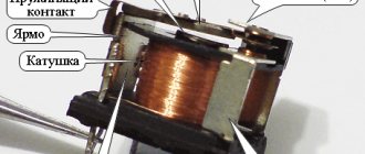
The filter is based on a choke made of two windings on one core.
Chokes can be made in different sizes, wound with thick or thin wire on large or small cores.
It is enough for a novice master to remember a simple rule: a filter with a large magnetic circuit inductor, an increased number of turns and a wire cross-section works better. (Principle: the more, the better.)
The inductor has inductive reactance, which sharply limits the high-frequency signal flowing through the phase or zero wire. At the same time, it does not have much effect on the current in the household network.
The operation of the inductor is effectively complemented by capacitive reactances.
The capacitors are selected in such a way that they short-circuit the interference signals weakened by the RF choke, directing them to ground potential.
The principle of operation of the filter for high-frequency noise from penetration of input signals into the power supply is shown in the picture below.
Y capacitors are installed between the ground potentials with zero and phase. Their design feature is that in the event of a breakdown they are not capable of creating an internal short circuit and supplying 220 volts to the device body.
Between the phase and zero circuits, capacitors are placed that can withstand 400 volts, or better yet, 630. They are usually shaped like a parallelepiped.
However, you should be well aware that the UPSs in the voltage converter themselves correct the signal and interference practically does not interfere with them. Therefore, such a system is relevant for conventional analog blocks with output signal stabilization.
For a switching power supply, it is important to prevent RF interference from entering the household network. Another solution implements this feature.
As you can see, the principle is the same. It’s just that capacitive reactances are always located along the path of the interference behind the inductor.
The third circuit of the high-frequency filter is considered universal. She combined elements of the first two. The Y capacitors in it simply work on both sides of each inductor.
The most expensive and reliable devices use a complex filter with additionally connected chokes and capacitors.
I immediately show the arrangement of filters on all circuits of the power supply: input and output.
Please note that a ferrite filter, consisting of two detachable half-cylinders or made of a one-piece structure, can be additionally installed on the cable coming out of the UPS and connected to the electronic device.
An example of its use is a switching power supply for a laptop. This is already the fourth use of the filter.
▍ Blocking generator
I had the highest hopes for this voltage source; it is very simple, miniature, and requires a minimum number of parts.
The only thing is that he needs a scarce TN30-220-400 transformer or needs to wind the transformer himself. Fortunately, we managed to find the transformer at a flea auction somewhere in Omsk. It all started with a comment from radiolok
... But the blocking generator can handle this quite well. I decided to take the TN30-220-400 transformer as a basis. 4 windings of 6.3V each will act as a primary, 13.5W of output power, the hardware is already designed for 400Hz.
There was an explanation below in the thread:
transistor T2 and then throw it out, put TN30-220-400 as Tr1. Of the 4 windings at 6.3V, we parallel three of them - this will be the main w2, the second - on the OS (w1) the former primary will become the secondary. The power will already be 5-6V.
I will say right away that there was no point in combining the windings, this does not affect the operation of the circuit in any way (which is logical), and the current is limited by a resistor (R1 in the diagram below), and even in the worst case it will not exceed the rated current of one winding. But I honestly tested this option, combining the windings, then disconnecting them (well, we need to test the hypothesis). In order not to confuse the reader, I will give another, more visual diagram from the same book by A.V. Kasimenko “Electroluminescent alphanumeric indicators.”
My supply voltage is adjustable. Resistor R1 limits the current that flows through the transformer winding and the transistor. Resistor R2 and capacitor C determine the period of operation of this generator, according to the following formula (from the same book):
Thus, the frequency is: If we take resistor R2 = 50k, leave the capacitor the same, then as a result we get a frequency of 400 Hz, as we need.
When I was selecting a transistor, I didn’t bother too much, I opened a well-known website and chose the first NPN transistor that caught my eye, 140 MHz, 160 V, 1.5 A - 2SB649AC
.
I would like to note one point that the above book uses homemade transformers with certain parameters, and not factory-made solutions. In general, winding a transformer is no problem, you just need time and patience. However, I have neither ferrite, nor winding wire, nor patience, so I decided to make do with what I have.
I will give a diagram of the transformer TN30-220-400
. Pay attention to the points in the blocking oscillator circuit from the book, and to the points in the transformer circuit. If you turn them on in antiphase, it will not work.
Transformer circuit.
Winding 3-4 acted as winding W1, winding 5-6 acted as winding W2. Secondary winding W3, respectively 1-2. At the output of the winding I installed a current-limiting resistor of 1 kOhm.
We assemble the entire circuit on a breadboard and carry out tests. No matter how much I struggled, with the parameters of resistor R2 and capacitor giving 400 Hz, I was unable to ignite a single segment of the ELI, only broken single points sometimes ignited. The only thing that managed to somehow light up was a neon light bulb.
The neon lamp glows faintly.
Single pulses are visible, the period between them is actually 400 Hz, but there is a very long period of just silence. As I understand it, this is determined by the inductance of the winding, because the parameters of the resistor-capacitor determined only the frequency of the pulses. After fiddling around with this simple circuit for several evenings, I came up with a rating of R2 = 10 kOhm (as in the circuit from the book in this post) - this is the 20 kHz frequency that the generator produces, and it is at the frequency limit of the transformer’s bandwidth. With these values, I even managed to light the IN-12A indicator lamp.
The oscillogram of the received signal is as follows (the divisor is 1:10).
In fact, a separate article could be written about just one blocking generator, with a bunch of measurements, oscillograms and other things. But I didn’t get any reasonable results from it, despite the simplicity of the solution. Most likely the transformer is not suitable for this task, perhaps I did something wrong. In any case, the output current is incredibly low, and the voltage sags from any minimal load, even such as a single segment
IEL.
Mains voltage rectifier: the most popular design
During the electrical conversion, the shape of a sine wave, consisting of half-waves of opposite signs, first changes to a signal in a positive direction after the diode assembly, and then these pulsations are smoothed out to an almost constant amplitude value of 311 volts.
Such a network voltage rectifier is included in the operation of all power supplies.
▍ We make a DC-AC converter on Arduino from available materials
As I already said, an incandescent transformer is not exactly a rarity, but it is unlikely that you have one at home. And the voltage of 6.3 volts is quite rare today. But exactly what you have at home is a 12 V transformer, from some old power supply. For example, from this:
As a result, to assemble a step-up DC-AC converter we will need:
- Arduino
- L298N motor driver
- Power supply, ideally adjustable, but suitable for 12 V
- Transformer power supply 12 V
On the topic of power supplies, everything is simple, if you find a 9-volt power supply, then you will need to power the entire circuit from 9 V.
We check that the power supply is working, and then we disassemble it. These adapters are simply glued together, and they must be disassembled in the same way as a coconut: along the perimeter, right along the seam, we tap with a hammer, when a gap appears, we insert a flat-head screwdriver into it and open it. If you get the hang of it, you can disassemble it, completely preserving the body.
Opened power supply.
The power supply is very simple: a transformer, a diode bridge at the output and a filter on one capacitor. We no longer need the scarf with the diode bridge and capacitor and can safely solder it.
Next, we collect everything according to the following scheme:
We upload the firmware, and everything should work right out of the box.
Neon lamp glows.
The voltage in this case is 210 V. Since I have an regulated power supply, this is not a problem.
It is very interesting to see the oscillograms of the operation of this device. Please note that the amplitude value of the meander voltage coincides with the effective value.
Oscillogram of idle speed.
Blue color is the voltage at the input of the transformer, yellow is the voltage at the output. Emissions are visible when changing the “smoker’s meander” phase. Related to the transformer capacity. But it goes away immediately when a small load is applied. An example of the same oscillogram when connecting a neon lamp.
Oscillogram under load.
The converter turned out to be quite powerful, and is even able to light a lamp. Although my power supply had difficulty carrying such a load, and it dropped well in current and voltage. But the lamp was shining.
More serious load.
It is also interesting to look at the resulting oscillogram.
A voltage drop is visible.
It is very interesting how the transformer copes with higher harmonics, passing them through without any problems. Let me remind you of my article “Harmonic Oscillations,” where I talked in detail about how many harmonics there are in a meander. This suggests that this transformer is quite suitable for use as an audio transformer.
Pulse voltage converter: explanation in simple words with explanatory pictures
The power switch is made by the primary winding of a high-frequency transformer. For effective transformation of high-frequency pulses up to 100 kilohertz, the magnetic core structure is made of alsifer or ferrites.
The transformer winding receives signal pulses of several tens of kilohertz from the control circuits through an RF transistor.
Rectangular current pulses are supplied in time, alternating with pauses, and are designated by one (1) and zero (0).
The duration of the pulse or its width at each moment of low-frequency sinusoidal voltage corresponds to its amplitude: the larger it is, the wider the PWM. And vice versa.
The PWM controller monitors the value of the connected load at the output of the switching power supply. According to its value, it generates pulses that briefly open the power transistor.
If the power connected to the UPS begins to increase, then the control circuit increases the duration of the control pulses, and when it decreases, it decreases.
Due to the operation of this design, the voltage at the output of the unit is stabilized in a strictly defined range.
▍ How it all began
I first came across electroluminescent indicators (hereinafter referred to as ELI) back in childhood, when my uncle showed how it works by simply poking wires into a socket. But then I had neither knowledge nor skills, but the desire to deal with them remained. Then radiolok started posting a bunch of videos on his live channel about his experiments with these indicators. As a result, I got excited and bought several IEL-0-IX 131-27
. Control unit indicators, their performance is unknown, and how to check is also unclear. They require power supply ~220V 400Hz, and best of all 1200Hz 180V. The first thought is to try sticking it into a socket to check its functionality. When I did this, a breakdown of one segment immediately occurred before my eyes, because our outlet has a 230 V standard, and the amplitude value will be higher not by 10 V, but by 14! We'll figure out why this happens a little later. As a result, I was faced with the problem of creating my own regulated power supply for these devices.
Indication devices where high voltage is required.
In fact, not only ELs require high voltage, but also, for example, electronic light paper (aka EL paper), also requires high alternating voltage for its power supply, and in fact is also EL, only without a pattern. She's on the left in the photo. Neon lamps are also powered by high voltage, but if for a neon lamp it is not very important whether it is constant or alternating, then for the IN-12A gas-discharge indicator lamp, I still recommend using constant voltage. When alternating, capacitive effects begin, and the discharge “jumps” from digit to digit.
To summarize: it is necessary to make an alternating voltage source with an output frequency of 400 Hz and an effective voltage value of 220 V.
Pulse transformer: operating principle of one pulse in 2 cycles
During the conversion of electrical energy to magnetic energy and back to electrical energy with reduced voltage, galvanic separation of the primary input circuits from the secondary output circuit is ensured.
Each PWM current pulse arriving when the power transistor is briefly opened flows through the closed circuit of the primary winding of the transformer.
Its energy is spent:
- first to magnetize the magnetic core;
- then to demagnetize it with current flowing through the secondary winding and additional charging of the capacitor.
According to this principle, each PWM pulse from the primary network recharges the storage capacitor.
UPS generators can operate using simple single-cycle or more complex push-pull construction technology.
Single-cycle switching power supply circuit: composition and principle of operation
On side 220 there are: a fuse, a rectifying diode bridge, a smoothing capacitor, a bipolar transistor, chains of an oscillating circuit and collector current, as well as windings of a pulse transformer.
A single-cycle switching power supply circuit is created to transmit power of 10÷50 watts, no more. It is used to make chargers for mobile phones, tablets and other digital gadgets.
The rectifier diode D7 is used in the output circuit of the transformer. It can be turned on in the forward direction, as shown in the picture, or reverse, which is important to consider.
When connected directly, the pulse transformer accumulates inductive energy and transfers it to the output circuit to the connected load with a time delay.
If the diode is turned back on, then the transformation of energy from the primary circuit to the secondary circuit occurs during the off state of the transistor.
The single-cycle UPS circuit is characterized by its simplicity of design, but large voltage amplitudes applied to the turns of the primary winding of the pulse transformer.
Their protection is carried out by additional chains of resistors R2÷R4 and capacitors C2, C3.
Push-pull switching power supply circuit: 3 design options
Higher efficiency and reduced power losses are the undeniable advantages of these UPSs compared to single-cycle models.
The simplest version of the full-wave technique is shown in the picture.
If you additionally connect two diodes and one smoothing capacitor to it, then a bipolar circuit is obtained using the same transformer.
It is common in power amplifiers and operates on the flyback principle. In it, smaller currents flow through each capacitor, providing an increased service life of the capacitors during operation.
The forward-flow power supply circuit has a choke in its design, which performs the function of energy storage. To do this, two diodes direct incoming PWM pulses to its input in the same polarity.
The choke of these devices is made in large dimensions and is installed separately inside the UPS board. It complements the operation of the storage capacitor.
This is clearly visible in the upper form of the signal shown by the rectification oscillogram of the same block without and with a choke.
The forward circuit is used in high-power power supplies, for example, inside a computer.
It uses Schottky diodes to rectify the current. They are used due to:
- reduced voltage drop on direct connection;
- and increased speed when processing high-frequency pulses.
3 diagrams of power stages of push-pull UPSs
In order of complexity of their implementation, generators perform the following:
- half-bridge;
- pavement;
- or the push-pull principle of constructing the output stage.
Half-bridge switching power supply circuit: overview
Capacitors C1, C2 are assembled in series with a capacitive divider. A constant supply voltage is supplied to it and the collector-emitter transitions of transistors T1, T2.
The primary winding of transformer Tr2 is connected to the midpoint of the capacitive divider and transistors. The output voltage of the generator is removed from its secondary winding, which is proportional to the input signal TP1, transformed to the bases T1 and T2.
The half-bridge UPS circuit works for loads ranging from a few watts to kilowatts. Its disadvantage is the possibility of damage to elements during overloads, which requires the use of complex protections.
Bridge Switching Power Supply Circuit: Brief Explanation
Instead of the capacitive divider of the previous technology, transistors T3 and T4 work here. They open in pairs together with T1 and T2: (pair T1-T4), (pair T2-T3).
The voltage of the emitter-collector transitions for closed transistors is not higher than the value of the supply voltage, and on the winding w1 TP3 it increases to the value U supply. Due to this, the efficiency value increases.
The bridge circuit is difficult to set up due to difficulties in setting up the control circuits of transistors T1÷T4.
Push-pull circuit: important features
The primary winding of the output TP2 has a middle terminal, to which the positive potential of the power source is supplied, and its minus is applied to the middle point of the secondary winding T1.
During the passage of one half-cycle of oscillation, one of the transistors T1 or T2 and the corresponding part of the transformer half-winding operate.
Here the highest efficiency, low ripple and low interference are created. The amplitude value of the pulse voltage on any half of the winding w1 TP2 reaches the value U power.
The self-inductive emf is added to the collector-emitter junction voltage of each transistor, and it increases to 2U power supply. Therefore, T1 and T2 must be selected at 600÷700 volts.
The push-pull circuit of the key cascade is more popular. It is used in the most powerful converters.
A graduate student from the Kazan Faculty of Science proposed a way to combine microwave-KFN graduate student proposed a way to combine microwave and power technologyToday, GaN device manufacturers often face challenges when creating normally-off GaN transistors, since they are typically normally-open devices. In her project “Technology and modeling of normally-open and normally-closed transistors for monolithic ICs based on GaN/Si structures,” postgraduate student of the Department of Quantum Physics and Nanoelectronics Olga Chukanova proposed an improved method for creating a normally-closed GaN transistor with a p-gate and considered solving problems organizing such a retreat.
“Creating a monolithic IC based on GaN structures allows us to solve problems with gate control and protection circuits, reduce assembly time and simplify it, and also allows us to create reliable drivers,” says Olga. – Also in this project we are exploring the possibility of forming devices with different gate lengths in a single technological cycle (which will allow us to combine microwave and power technologies). Thanks to the possibility of forming two types of devices of different configurations on one wafer, it is possible to create digital monolithic integrated circuits, thereby expanding the electronic component base of Russia.” At the moment, together with scientific supervisor Vladimir Ilyich Egorkin, Olga Chukanova has already developed technologies for the formation of normally-open transistors and the technology of normally-closed transistors with a p-gate. “We are currently working on mathematical modeling in Sentaurus TCAD of transistors with various device configurations,” explains the graduate student. “Having received good modeling results, we plan to move on to experimental testing of the possibility of combining two technologies in a single technological cycle.”
Olga’s work is a continuation of the project “Technology development and technological preparation for the production of transistor crystals based on gallium nitride heterostructures on a silicon substrate with a diameter of 150 mm for power converter modules,” which was created jointly with the Zelenograd Nano-Technology Center (ZNTC). The first presentation of this project was presented at the “Scientific Internship” competition from the Sintez Foundation by Gennady Komissarov, where Olga received the highest award.
After this victory, in the summer of 2022, the KFN graduate student completed an internship at the ZNTC. “Thanks to this competition, last December I was invited to a scientific congress in the educational one in Sochi, which was dedicated to the year of science and technology. At the congress, I was given the opportunity to announce my scientific achievements by making a presentation at the “Russia – Land of Opportunities” stand. Of course, I didn’t miss this opportunity.”
Let us recall that the congress at Sirius became one of the key events of the Year of Science and Technology, announced on the initiative of Russian President Vladimir Putin. It included round tables, sessions, and discussions dedicated to the results of the thematic months of the Year of Science and Technology and the VIII Annual National Exhibition “Vuzpromexpo”. Educational events were also organized in various areas of research activities. Olga gave a presentation about her project, the speech was highly appreciated by experts.
Among the experts of the Congress of Young Scientists were Dmitry Chernyshenko, Deputy Chairman of the Government of the Russian Federation, Andrey Fursenko, Assistant to the President of the Russian Federation, Valery Falkov, Minister of Science and Higher Education of the Russian Federation, Anton Kobyakov, Advisor to the President of the Russian Federation. Alexander Sergeev, President of the Russian Academy of Sciences, also took part in the work of the Congress.
“Previously, I also presented my project at the international forum “Power Electronics - 2021” in October 2022. Then the project “Technology and modeling of normally-open and normally-closed transistors for monolithic ICs based on GaN/Si structures” brought us victory in the competition “Umnik. Project team – electronics.”
The estimated completion date for the project is the end date of the contract with the Innovation Promotion Fund for the “Umnik” competition. This is the end of 2022. Scientists suggest that the chances of combining the two technologies using developments within the project are quite high. “Perhaps we will soon begin developing a digital monolithic circuit,” says Olga. – But you shouldn’t think too far. In our field, big goals are usually achieved in small steps!” Comments: 0
Voltage stabilization circuit: how it works
The most primitive output voltage stabilization circuit is created on the additional winding of a pulse transformer.
The voltage is removed from it and applied to adjust the signal value of the primary winding.
Better stabilization is created by monitoring the output signal from the secondary winding and separating its galvanic connection through an optocoupler.
It uses an LED through which a current passes proportional to the output voltage. Its glow is perceived by a phototransistor, which sends a corresponding electrical signal to the control circuit of the key stage generator.
The quality of output voltage stabilization can be improved by sequentially adding a zener diode to the optocoupler, as shown in the example of the TL431 microcircuit in the picture below.
To consolidate the material in your memory, I recommend watching the video of the owner of Soldering Iron TV, which explains well the information about switching power supplies: operating principles using the example of a specific model.
I hope that my article will help you repair your UPS yourself in 7 steps, which I outlined in another article.
Ask any questions you have in the comments section and express your opinion. It will be useful for other people to know it.