A semiconductor diode has many “professions”. It can rectify voltage, decouple electrical circuits, and protect equipment from improper power supply. But there is an unusual type of “work” of a diode, when its property of one-way conductivity is used very indirectly. A semiconductor device for which the normal mode is reverse bias is called a zener diode.
Types of diodes
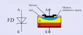
A zener diode (Zener diode) is a type of semiconductor diode that operates at a reverse bias voltage in breakdown mode.
Until breakdown occurs, very insignificant leakage currents flow through the zener diode, and its resistance is quite high. At the moment of breakdown, the current through it increases sharply, and its differential resistance decreases to small values. Due to this, in the breakdown mode, the voltage on the zener diode is maintained with good accuracy in a wide range of reverse currents. The main separation of diodes occurs according to their type. There are three categories: material of manufacture, pn junction area and purpose.
Material
To produce diodes, one of four initial semiconductors is used:
- germanium - in low-power and precision circuits, has a higher transmission coefficient;
- silicon – inexpensive and durable, resistant to temperature, but less conductive;
- gallium arsenide – more expensive and more complex than silicon, high radiation resistance;
- indium phosphide - in LEDs and for operation at ultrahigh frequencies.
Each material in different systems has its own letter or number, which is indicated at the beginning.
Transition area
There are two options for the structural placement of the cathode and anode:
- Point diode. One of the electrodes in the form of a narrow needle is fused into the crystal, forming a pn boundary. It has a small area, which results in a high operating frequency. They are almost out of use due to low strength, vulnerability to overloads and low maximum current.
- Planar diode. The transition area is larger - the contact passes over the area of the semiconductor wafer connected to the crystal. They are distinguished by higher capacity, low noise level, and low voltage drop. An example is a Schottky diode.
In modern marking, separation practically does not occur - planar diodes are gradually replacing point diodes.
Subtype
The following designation depends on the purpose of the device. There is a classification of diodes used in different areas: tunnel, laser, varicaps, zener diodes. There is also a division within the subtype , based on technical parameters:
- operating frequency;
- recovery time;
- forward and reverse current;
- permissible values of reverse and forward voltage;
- temperature regime.
This results in a large number of possible combinations, hence the difficulty of creating a unified labeling system.
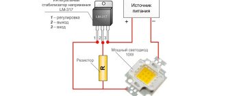
Increasing the power of the parametric stabilizer
The maximum output power of the simplest parametric voltage stabilizer depends on the values of Ist.max and Pmax of the zener diode. The power of a parametric stabilizer can be increased if a transistor is used as a regulating component, which will act as a DC amplifier.
Parallel stabilizer
PSN circuit with parallel connection of a transistor
The circuit is an emitter follower; a load resistance RH is connected in parallel with the transistor VT. Ballast resistor R1 can be included in both the collector and emitter circuits of the transistor. The load voltage is
The scheme works as follows. As the current through the resistor RH increases, and accordingly the voltage (U1 = UCT) at the output of the stabilizer, the base-emitter voltage (UEB) and collector current IK increase, since the transistor operates in the amplification region. An increase in the collector current leads to an increase in the voltage drop across the ballast resistor R1, which compensates for the increase in voltage at the output of the stabilizer (U1 = UCT). Since the zener diode current ICT is also the base current of the transistor, it is obvious that the load current in this circuit can be h21e times greater than in the simplest parametric stabilizer circuit. Resistor R2 increases the current through the zener diode, ensuring its stable operation at the maximum value of the coefficient h21e, the minimum supply voltage U0 and the maximum load current IN.
The stabilization coefficient will be equal to
where RVT is the input resistance of the emitter follower
where Re and Rb are the resistances of the emitter and base of the transistor.
Resistance Re depends significantly on the emitter current. As the emitter current decreases, the resistance Re increases rapidly and this leads to an increase in RVT, which worsens the stabilizing properties. The Re value can be reduced by using high-power transistors or composite transistors.
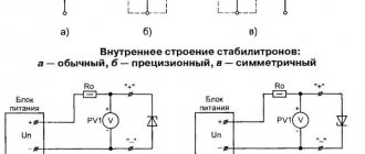
The principle of operation of a zener diode
Let's consider the principle of operation of a zener diode using the example of its connection circuit and current-voltage characteristic. To perform its main function, the zener diode VD is connected in series with a resistor Rb and together they are connected to a source of unstabilized input voltage Uin. The already stabilized output voltage Uout is removed only from pins 2, 3 VD. Therefore, the load Rн is connected to the corresponding points 2 and 3. As can be seen from the diagram, VD and Rb form a voltage divider. Only the resistance of the zener diode does not have a constant value and is called dynamic, since it depends on the amount of electric current flowing through the semiconductor device.
The voltage Uin supplied to the zener diode from the resistors must be at least a couple of volts higher than the output voltage Uout, otherwise the semiconductor device VD will not open and will not be able to perform its main function.
Let's say that at some arbitrary point in time at outputs 1 and 3 the value of Uin began to increase. The following processes will begin to occur in the circuit. As the voltage increases, according to Ohm's law, the current will begin to increase, let's call it the input current Iin. As the current increases, the voltage drop across the resistor Rb will increase, and at VD it will remain unchanged (this will be explained further in the characteristic), therefore Uout will remain at the same level. Consequently, the increase in input voltage will drop or be extinguished by resistor Rb. Therefore, Rb is called damping or ballast.
Now, let’s say the load has changed, for example, the resistance Rн has decreased, and the current In will increase accordingly. In this case, the current flowing through the zener diode Ist will decrease, and Iin will remain virtually unchanged.
How to check zener diode
You can check the zener diode for serviceability quite simply and quickly using a simple multimeter. To do this, the multimeter should be switched to the “continuity” mode, usually indicated by a diode sign. Then, if we touch the anode with the positive probe of the multimeter, and the cathode with the negative probe, then on the display of the measuring device we will see a certain value of the voltage drop across the pn junction. Since direct voltage is applied to the semiconductor device (see the direct branch of the current-voltage characteristic), the reference diode will open.
Now, if the probes of the multimeter are swapped, thereby applying reverse voltage to the terminals of the semiconductor device (see the reverse branch of the current-voltage characteristic), then it will be locked and will not conduct current. The meter display will show a unit, indicating infinitely high resistance.
If in both cases the multimeter shows one or rings, then the zener diode is unusable.
How to distinguish a stabilization diode from a conventional semiconductor
Very often people wonder how they can distinguish a zener diode from a standard semiconductor, because, as we found out earlier, both of these elements have almost identical symbols on the electrical circuit and can perform similar functions. The easiest way to distinguish a stabilization semiconductor from a regular one is to use a multimeter attachment circuit. With its help, you can not only distinguish both elements from each other, but also identify the stabilization voltage, which is characteristic of a given SMD (if it, of course, does not exceed 35V). The multimeter attachment circuit is a DC-DC converter, in which there is galvanic isolation between the input and output. This diagram looks like this:
Multimeter attachment circuit
In it, a generator with pulse-width modulation is implemented on a special microcircuit MC34063, and to create galvanic isolation between the measuring part of the circuit and the power source, the control voltage should be removed from the primary winding of the transformer. For this purpose there is a rectifier on VD2. In this case, the value for the output voltage or stabilization current is set by selecting resistor R3. A voltage of approximately 40V is released at capacitor C4. In this case, the tested SMD VDX and the stabilizer for current A2 will form a parametric stabilizer. The multimeter, which is connected to terminals X1 and X2, will measure the voltage at this zener diode. When connecting the cathode to the “-” and the anode to the “+” of the diode, as well as to the asymmetrical SMD of the multimeter, the latter will show a slight voltage. If you connect in reverse polarity (as in the diagram), then in a situation with a conventional semiconductor, the device will register a voltage of about 40V.
Note! For symmetrical SMD, the breakdown voltage will appear in the presence of any connection polarity.
Here the T1 transformer will be wound on a torus-shaped ferrite core with an outer diameter of 23 mm. Such winding 1 will contain 20 turns, and the second winding will contain 35 turns of PEV 0.43 wire. In this case, it is important to lay the turn to the turn when winding. It should be remembered that the primary winding goes on one part of the ring, and the second on the other. When setting up the device, connect a resistor instead of smd VDX. This resistor should have a value of 10 kOhm. And resistance R3 needs to be selected in order to achieve a voltage of 40V on capacitor C4. This is how you can find out whether you have a zener diode or a regular diode.
Designations for the operation of an electrical circuit element
Schematic designation of a zener diode
Since the zener diode is a special diode, its designation is no different from them. Schematically, smd is designated as follows:
A zener diode, like a diode, has a cathode and anode part. Because of this, there is direct and reverse inclusion of this element.
Turning on the zener diode
At first glance, the inclusion of such a diode is incorrect, because it should be connected “the other way around”. In a situation where reverse voltage is applied to the SMD, the phenomenon of “breakdown” is observed. As a result, the voltage between its terminals remains unchanged. Therefore, it must be connected in series to a resistor in order to limit the current passing through it, which will ensure that the “excess” voltage from the rectifier drops.
Note! Each diode designed to stabilize voltage has its own “breakdown” (stabilization) voltage and also has its own operating current.
Due to the fact that each zener diode has such characteristics, it is possible to calculate the value of the resistor that will be connected in series with it. For imported zener diodes, their stabilization voltage is presented in the form of markings on the body (glass or not). The designation of such an smd diode always begins with BZY... or BZX..., and their breakdown (stabilization) voltage is marked V. For example, the designation 3V9 stands for 3.9 volts.
Note! The minimum voltage for stabilization of such elements is 2 V.
Details about the color coding of the stabilizing diode
Zener diode marking
Any diode (zener diode, etc.) contains a special marking on its case, which reflects what material was used to manufacture each specific semiconductor. Such marking may look like this:
- letter or number;
- letter.
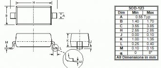
In addition, the marking reflects the electrical properties and purpose of the device. Usually a number is responsible for this. The letter, in turn, reflects the corresponding type of device. In addition, the marking contains the date of manufacture and the symbol of the product. Integral type SMDs often contain full markings. In such a situation, there is a conditional code on the product body that indicates the type of microcircuit. An example of decoding the code markings for microcircuits applied to the housing is shown in the figure:
Example of microcircuit marking
In addition, there is also color coding. It exists in several versions, but the most commonly used is the Japanese marking (JIS-C-7012). The color coding is shown in the following table.
Zener diode power dissipation
The power dissipation of a zener diode Pst characterizes its ability not to overheat above a certain temperature for a long time. The higher the Pst value, the more heat the semiconductor device can dissipate. The dissipation power is calculated for the most unfavorable operating conditions of the device, therefore, the maximum possible Uin and the smallest values of Rb and In are substituted into the formula below:
There are a number of standard ratings for this parameter: 0.3 W, 0.5 W, 1.3 W, 5 W, etc. The larger Pst, the larger the dimensions of the semiconductor device.
A little more about the module and how it works
This is a semiconductor diode that has the property of producing a certain voltage value regardless of the current supplied to it. This statement is not completely true for absolutely all options, because different models have different characteristics. If you apply a very strong current to an SMD module (or any other type) that is not designed for this purpose, it will simply burn out. Therefore, the connection is made after installing a current-limiting resistor as a fuse, the value of the output current of which is equal to the maximum possible value of the input current to the stabilizer.
Schemes for connecting a zener diode and a stabilistor to a circuit
It is very similar to an ordinary semiconductor diode, but has a distinctive feature - its connection is done in reverse. That is, the minus from the power source is supplied to the anode of the zener diode, and the plus to the cathode. Thus, a reverse branch effect is created, which provides its properties.
A similar module is a stabistor - it is connected directly, without a fuse. It is used in cases where the parameters of the input electricity are precisely known and do not fluctuate, and the output also produces an exact value.
What is a zener diode, where is it used and what are they?
A zener diode, or Zener diode (named after the American scientist who was the first to study and describe the properties of this semiconductor device), is a conventional diode with a pn junction. Its peculiarity is that it operates in the characteristic section with a negative bias, that is, when the voltage is applied in reverse polarity. Such a diode is used as an independent stabilizer that maintains the consumer voltage constant, regardless of changes in the load current and fluctuations in the input voltage. Zener diode units are also used as reference voltage sources for other stabilizers with a developed circuit. Less commonly, a reverse-connected diode is used as a pulse-forming element or a protective surge suppressor.
There are regular zener diodes and two-anode ones. A two-node zener diode is two diodes connected back-to-back in one housing. It can be replaced by two separate devices by connecting them according to the appropriate circuit.
Marking of zener diodes
Markings are applied to the zener diode housing in the form of numbers and letters (or letters). There are fundamentally two different types of markings. The zener diode in a glass case has the usual markings for us, directly indicating the rated stabilization voltage. The numbers can be separated by the letter V, which acts as a decimal point. For example, 5V1 means 5.1 V.
A less clear way of marking consists of four numbers and a letter at the end. If you are not an experienced radio amateur, then you can’t do without a datasheet. For example, let's decipher the parameters of the reference diode of the 1N5349B series. We are most interested in the first column, which shows the rated voltage of 12 V. The second column is the rated current value - 100 mA.
The cathode of a zener diode of any type is indicated by a black or blue ring, which is applied to the body from the side of the corresponding terminal.
Additional markings for glass models
Diodes in glass cases have their own designations, which we will consider below. They are so simple (unlike options with plastic cases) that they are almost immediately memorized by heart; there is no need to use a reference book every time.
Color coding is used for plastic diodes, such as SOT-23. The solid body of the module has two flexible leads. On the case itself, next to the stripe described above, several numbers are written in the same color, separated by a Latin letter. Usually the record looks like 1V3, 9V0, and so on, the variety allows you to select any parameters according to the designation, as in SMD.
What does this code marking mean? It shows the stabilization voltage for which this element is designed. For example, 1V3 shows us that this value is 1.3 V, while the second option is 9 volts. Typically, the larger the body itself, the greater the stabilizing property it has. The photo below shows a zener diode in a glass case with a 5.1 V cathode marking
Labeled zener diode
Marking of foreign zener diodes
The designation of foreign zener diodes, as well as diodes, is carried out according to two popular standards JEDEC and PRO ELECTRON. Since everything is described in detail in the article on marking diodes, I see no point in repeating this information; I will only dwell on some of the features.
Marking of zener diodes in a glass case with flexible leads is carried out in a very clear way. Typically, numbers are applied to the body, separated by the Latin symbol “V”. For example, 4V7 indicates a stabilization voltage of 4.7 Volts; 9V1, respectively 9.1 V, etc.
The black ring on the body of glass zener diodes is the negative terminal (cathode).
Features of color marking of zener diodes.
When marking smd zener diodes, colored rings are used. Similar markings are also used for domestic zener diodes, but more on that below. In foreign SMD zener diodes, the color ring is applied from the cathode side. Information on decoding color rings can be found in the same article above on diode markings or in the reference manual on SMD component markings (to download it, you need to click on the green arrow, just above).
Some companies manufacture SMD zener diodes with three terminals, while one of them is not used. You can determine the excess one using a multimeter.
| Color marking of domestic zener diodes and stabilizers |
| Diode type | Mark at the cathode terminal | Mark at the anode terminal | Drawing |
| D814A1 | — | black wide ring | |
| D814B1 | — | black wide+black narrow ring | |
| D814V1 | — | black narrow ring | |
| D814G1 | — | yellow wide ring | |
| D814D1 | — | three narrow black rings | |
| D818A | black mark on the end of the case + white ring | — | |
| D818B | black mark on the end of the case + yellow ring | — | |
| D818V | black mark on the end of the case + blue ring | — | |
| D818G | black mark on the end of the case + green ring | — | |
| D818D | black mark on the end of the case + gray ring | — | |
| D818E | black mark on the end of the case + orange ring | — | |
| KS107A | gray mark on the end of the case + red ring | — | |
| KS126A | red wide+purple narrow+white narrow rings | — | |
| KS126B | orange strip + black narrow + white narrow ring | — | |
| KS126V | orange wide+orange wide+white narrow rings | — | |
| KS126G | orange wide+white narrow+white narrow rings | — | |
| KS126D | yellow wide+purple narrow+white narrow rings | — | |
| KS126E | green wide+blue narrow+white narrow rings | — | |
| KS126ZH | blue wide + red narrow + white narrow rings | — | |
| KS126I | blue wide+gray narrow+white narrow rings | — | |
| KS126K | purple narrow+green narrow+white narrow rings | — | |
| KS126L | gray wide+red narrow+white narrow rings | — | |
| KS126M | white wide+brown narrow+white narrow rings | — | |
| KS207A | brown wide+black narrow+black narrow rings | — | |
| KS207B | brown wide+brown narrow+black narrow rings | — | |
| KS207V | brown wide+red narrow+black narrow rings | — | |
| KS133A | blue ring | white ring | |
| 2С133А | white ring | black ring | |
| KS133G | orange mark on the end of the case | — | |
| KS139A | green ring | white ring | |
| 2С139А | green ring | black ring | |
| KS147A | gray or blue ring | white ring | |
| 2С147А | — | black ring | |
| KS147G | green mark on the end of the body | — | |
| KS156A | orange ring | white ring | |
| 2С156А | orange ring | black ring | |
| KS156G | red mark on the end of the body | — | |
| KS168A | red ring | white ring | |
| 2С168А | red ring | black ring | |
| KS175ZH | white ring | — | |
| KS182ZH | yellow ring | — | |
| KS191ZH | red ring | — | |
| KS210ZH | green ring | — | |
| KS211Zh | gray ring | — |
| Stabilizer type | Mark at the cathode terminals | Mark at the anode terminals | Drawing |
| KS212Zh | orange ring | — | |
| KS213Zh | black ring | — | |
| KS215Zh | white ring | black ring | |
| KS216ZH | yellow ring | black ring | |
| KS218Zh | red ring | black ring | |
| KS220Zh | green ring | black ring | |
| KS222Zh | gray ring | black ring | |
| KS224Zh | orange ring | black ring | |
| 2S175Zh | blue mark on the end of the case + white ring | — | |
| 2S182Zh | blue mark on the end of the body + yellow ring | — | |
| 2S191Zh | blue mark on the end of the case + red ring | — | |
| 2S210ZH | blue mark on the end of the case + green ring | — | |
| 2S211ZH | blue mark on the end of the case + gray ring | — | |
| 2S212ZH | blue mark on the end of the case + orange ring | — | |
| 2S213ZH | blue mark on the end of the case + black ring | — | |
| 2S215ZH | blue mark on the end of the case + white ring | black ring | |
| 2S216ZH | blue mark on the end of the body + yellow ring | black ring | |
| 2S218ZH | blue mark on the end of the case + red ring | black ring | |
| 2S220ZH | blue mark on the end of the case + green ring | black ring | |
| 2S222ZH | blue mark on the end of the case + gray ring | black ring | |
| 2S224ZH | blue mark on the end of the case + orange ring | black ring | |
| KS405A | gray mark on the end of the case + red ring | black ring | |
| KS406A | black mark on the end of the case + gray ring | white ring | |
| KS406B | black mark on the end of the case + white ring | orange ring | |
| KS407A | black mark on the end of the case + red ring | blue ring | |
| KS407B | black mark on the end of the case + red ring | orange ring | |
| KS407V | black mark on the end of the case + red ring | yellow ring | |
| KS407G | black mark on the end of the case + red ring | green ring | |
| KS407D | black mark on the end of the case + red ring | gray ring | |
| KS411A | white ring | black ring | |
| KS411B | blue ring | black ring | |
| KS508A | black mark on the end of the case + orange ring | green ring | |
| KS508B | black mark on the end of the case + yellow ring | white ring | |
| KS508V | black mark on the end of the case + red ring | green ring | |
| KS508G | black mark on the end of the case + blue ring | white ring | |
| KS508D | black mark on the end of the case + green ring | white ring | |
| KS510A | orange ring | green ring | |
| KS512A | yellow ring | green ring | |
| KS515A | white ring | green ring | |
| KS516A | green ring | black ring | |
| KS518A | blue ring | green ring | |
| KS522A | gray ring | green ring | |
| KS527A | black ring | green ring |
| How to check zener diode |
It is impossible to fully check it and say with 100% certainty that this zener diode is serviceable with a digital multimeter. Of course, it can be checked in the same way as a diode, but you can mistakenly consider the working zener diode to be damaged. Is this possible? Let's conduct a small practical experiment, take any zener diode with a small stabilization voltage, for example 2.4 volts. And we connect it to a digital multimeter, and it rings in both directions. But the trick is that there is about 5 volts on the digital multimeter probes, and therefore it simply breaks through in the opposite direction. Therefore, you should not check zener diodes with low stabilization voltage with digital multimeters; it is better to use an old analog tester, and if you don’t have one, you can assemble a small circuit.
Color coding of diodes in SOD-80 packages
The SOD-80 body, also known as MELF, is a small glass cylinder with metal leads.
Examples of diode markings.
Marking 2Y4 to 75Y (E24 series) BZV49 1W silicon zener diode (2.4 - 75V) Marking C2V4 to C75 (E24 series) BZV55 500mW silicon zener diode (2.4 - 75V)
The cathode terminal is marked with a colored ring.
Marking of devices with colored rings.
| Cathode output | Device |
| Black | BAS32, BAS45, BAV105 LL4148, 50, 51,53, LL4448 BB241,BB249 |
| Black and Kochichnevy (Black Brown) | LL4148, LL914 |
| Black and orange (Black Orange) | LL4150, BB219 |
| Brown and green | LL300 |
| Brown and black | LL4448 |
| Red | BA682 |
| Red and orange | BA683 |
| Red and green | BA423L |
| Red and White | LL600 |
| Orange and Yellow | LL3595 |
| Yellow | BZV55,BZV80,BZV81 series zeners |
| Green | BAV105, BB240 |
| Green and black (Green Black) | BAV100 |
| Green and nomadic (Green Brown) | BAV101 |
| Green and red (Green Red) | BAV102 |
| Green and orange | BAV103 |
| Gray | BAS81, 82, 83, 85, 86 |
| White | BB219 |
| White and green (White Green) | BB215 |
Some SMD diodes in MiniMELF (SOD80 / DO213AA / LL34) or MELF (DO213AB / LL41) cylindrical packages are often marked with colored stripes (the first stripe closest to the edge is located at the cathode) in accordance with the table on the left.
Zener diode color coding
To indicate the parameters of the zener diode, colored marks are used, made in the form of stripes encircling the body. The negative terminal (cathode) is indicated by a black (sometimes gray) stripe. It must be taken into account that for domestic parts the black ring can indicate both the cathode and the anode. On imported parts, the color rings are closer to the negative terminal.
The color (or combination of colors) of the stripes indicates the type of zener diode. This somewhat complicates the identification process, since you must first determine the type of zener diode itself, then find information about its parameters. However, the small size of the parts does not allow detailed information to be applied, so the issue has to be resolved in the most reliable way. The marking does not erase and does not change color when heated, which makes it possible to determine the rating and type of zener diode even after a short circuit of the device.
Indication of passport characteristics
They are also the main indicators of domestic and imported zener diodes, which must be used as a guide when selecting a zener diode for a specific electronic circuit.
- UCT – indicates what nominal value the module is capable of stabilizing.
- ΔUCT – used to indicate the range of possible incoming current deviation as a safe damping.
- ICT – parameters of the current that can flow when the rated voltage is applied to the module.
- ICT.MIN – shows the smallest value that can flow through the stabilizer. In this case, the voltage flowing through the diode will be in the range UCT ± ΔUCT.
- ICT.MAX – the module is not able to withstand a voltage higher than this value.
The photo below shows the classic version. Please note that right on the body it is shown where the anode and cathode are. A black stripe is drawn in a circle (more rarely, a gray stripe is found), which is located on the cathode side. The opposite side is the anode. This method is used for both domestic and imported diodes.
Marking the location of the cathode and anode
Main conclusions
Knowledge of the markings of SMD diodes and other components will help when performing repair work, identifying analogues or options for replacing parts. To obtain detailed information about the parameters of elements, you must use the following sources:
- directory of SMD component codes;
- datasheet (mainly for transistors);
- deciphering the code for resistors or chokes.
The number of SMD diodes and other parts is large. Many manufacturers develop their own marking system, which is in no way correlated with other designations, which introduces significant confusion into the process of identifying and replacing problematic elements. Therefore, it is important to have reference books and complete blocks of information on the parameters of diodes or other parts from different companies on hand.