Modern printed circuit boards look different from their predecessors. The familiar parts with legs inserted into holes have practically disappeared. They were replaced by very tiny components soldered on top of the board to specially created contact pads. They are called SMD (Surface Mounted Device, or surface-mounted device).
Such parts are much more convenient - the whole and very precise operation of drilling holes in the manufacture of the board is eliminated, and compactness is achieved. At the same time, their miniature size does not allow them to be labeled with a detailed and familiar name. The marking of SMD diodes is made in the form of codes, which need to be discussed in more detail.
Introduction
The modern radio amateur now has access to not only ordinary components with leads, but also such small, dark parts that you can’t understand what’s written on them.
They are called “SMD”. In Russian this means “surface mount components”. Their main advantage is that they allow the industry to assemble boards using robots that quickly place SMD components in their places on the printed circuit boards, and then mass bake them to produce assembled printed circuit boards. The human share remains with those operations that the robot cannot perform. Not yet. The use of chip components in amateur radio practice is also possible, even necessary, as it allows you to reduce the weight, size and cost of the finished product. Moreover, you practically won’t have to drill.
Another important quality of surface mount components is that, due to their small size, they introduce fewer parasitics. The fact is that any electronic component, even a simple resistor, has not only active resistance, but also parasitic capacitance and inductance, which can manifest itself in the form of parasitic signals or incorrect operation of the circuit
SMD components are small in size, which helps reduce parasitic capacitance and inductance of the component, therefore improving the performance of the circuit with small signals or at high frequencies.
For those who first encountered SMD components, confusion is natural. How to understand their diversity: where is the resistor, and where is the capacitor or transistor, what sizes do they come in, what types of SMD parts are there? You will find answers to all these questions below. Read it, it will come in handy!
Part Description
Externally, the electronic component is no different from an ordinary diode. Its miniature DO-201AD body is cylindrical in shape. It is made of heat-resistant black plastic. On the sides are two copper terminals called the anode and cathode. They are necessary to fix the 1N5822 on the printed circuit board and connect the part with other elements of the circuit. The terminals are covered with a thin layer of solder. If the part is new, then they have a characteristic silvery shine. After installing the diode in the desired location, the legs are shortened to the minimum size.
The part in question belongs to the category of so-called Schottky barrier diodes. Their main difference from conventional semiconductor rectifiers, like the 1N4007, is the low voltage drop when turned on in the forward direction. It is 0.2-0.4 V versus the typical 0.6-0.7 V for conventional silicon diodes.
This feature allows the 1N5822 Schottky diode to be used in circuits with higher currents. After all, the lower the voltage drop across the diode, the less power dissipated on it. This implies another advantage of this category of rectifiers. Their chip generates a small amount of heat, so the part body has smaller dimensions, and in some cases the use of radiators or forced cooling can be avoided.
Additional Information. By connecting two diodes in parallel, you can achieve an even smaller voltage drop. This in turn will double the maximum current allowed through such an assembly. This solution is often used by electronics manufacturers. Parts are also produced that already contain two diodes connected in parallel in one housing.
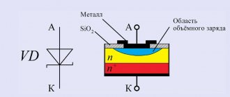
Another feature of Schottky diodes, incl. and 1N5822, follows from its structure. In this part, the usual electron-hole pn junction is replaced by a metal-semiconductor structure. This structure made it possible to significantly reduce the input parasitic capacitance of the element and, as a result, to use it in higher-frequency circuits.
Structure of a Schottky diode
SMD field effect transistors
| Marking | Device type | Marking | Device type |
| 6A | MMBF4416 | C92 | SST4392 |
| 6B | MMBF5484 | C93 | SST4393 |
| 6C | MMBFU310 | H16 | SST4416 |
| 6D | MMBF5457 | I08 | SST108 |
| 6E | MMBF5460 | I09 | SST109 |
| 6F | MMBF4860 | I10 | SST110 |
| 6G | MMBF4393 | M4 | BSR56 |
| 6H | MMBF5486 | M5 | BSR57 |
| 6J | MMBF4391 | M6 | BSR58 |
| 6K | MMBF4932 | P01 | SST201 |
| 6L | MMBF5459 | P02 | SST202 |
| 6T | MMBFJ310 | P03 | SST203 |
| 6W | MMBFJ175 | P04 | SST204 |
| 6Y | MMBFJ177 | S14 | SST5114 |
| B08 | SST6908 | S15 | SST5115 |
| B09 | SST6909 | S16 | SST5116 |
| B10 | SST6910 | S70 | SST270 |
| C11 | SST111 | S71 | SST271 |
| C12 | SST112 | S74 | SST174 |
| C13 | SST113 | S75 | SST175 |
| C41 | SST4091 | S76 | SST176 |
| C42 | SST4092 | S77 | SST177 |
| C43 | SST4093 | TV | MMBF112 |
| C59 | SST4859 | Z08 | SST308 |
| C60 | SST4860 | Z09 | SST309 |
| C61 | SST4861 | Z10 | SST310 |
| C91 | SST4391 |
If you are not sure that this is a transistor, or its decoding is not indicated here, see the link for a general table of all planar parts. What different SMD transistor packages look like is shown in the figure below:
And this is an example of npn and pnn bipolar transistors (sot-23, sot-323) with a typical pin arrangement:
Development of LED technologies of the 21st century
The light-emitting diode, or LED (light emitting diode), as it is commonly called in English, was able to make fundamental changes in the production of artificial lighting sources in the first decade of the new century. The smooth development of low-power LEDs quickly moved into the next phase - the development of “powerful” lamps based on the release of light energy due to processes in semiconductors.
The main impetus for action was the discovery of a white glow, initially based on the summation of three primary colors in a certain percentage. The world's major manufacturers of electronic equipment quickly understood the economic essence of this issue and, to this day, do not spare financial resources for the development of light-emitting equipment. Multimillion-dollar installations for the development of new samples and production of serial copies are already paying off, proving their advantage in practice. Today, every store specializing in the sale of “electricals” is able to offer LED products to potential buyers. As a rule, the assortment is represented by flashlights, decorative ribbons, spotlights and lamps for E14 and E27 standard sockets.
SMD (translated from English) is a surface mount device. In other words, SMD LEDs are a device made in a small housing with a built-in light-emitting crystal, which is surface mounted on a printed circuit board.
Round LED with fasteners.
But let's return to technology. Conventional emitting diodes in a 5 mm package could not realize all the technical ideas of engineers to increase the luminous flux and uniform heat dissipation. It was necessary to create a new semiconductor element format that could satisfy all the wishes of the developers. Thus, an SMD LED appeared, which was able to outperform its predecessors by an order of magnitude in all respects. Surface mounting technology or SMD technology (surface mounted device) originated in the 60s of the last century, but gained production momentum only 25 years later. The minimization of electronic equipment and the development of nanotechnology contributed to the abandonment of conventional radioelements with leads and the transition to surface mounting.
Table of wavelengths of smd 5050 LEDs, different luminescence
The creators of a new type of emitting diodes only needed to correctly position the semiconductor crystal on the substrate. Improving technological techniques and methods for designing printed circuit boards and expanding the element base have left their mark on the design of SMD diodes, expanding their scope of application. In particular, they were the first to replace body diodes used in outdoor advertising screens. Three-color SMD LEDs have increased image resolution several times. In addition, they are not afraid of moisture, which has led to a reduction in the cost of billboards.
Table of characteristics and sizes of popular SMD LEDs.
Color coding
Every radio amateur knows the difficulty of identifying diodes surrounded by a glass housing. One person. Sometimes the manufacturer bothers to apply clear marks and multi-colored rings. According to the notation system, three characteristics are introduced:
- Markers of cathode and anode areas.
- The color of the body, replaced by a colored dot.
According to the state of affairs, at first glance we can distinguish the types of diodes:
- The D9 family is marked with one or two colored rings in the anode area.
- KD102 diodes in the anode area are indicated by a colored dot. The case is transparent.
- KD103 have a color body that complements the dot, with the exception of 2D103A, which is indicated by a white dot in the anode area.
- The KD226, 243 families are marked with a cathode region ring. No other marks are provided.
- Two colored rings in the cathode area can be seen in the KD247 family.
- KD410 diodes are indicated by a dot in the anode area.
Other visible marks are present. You will find a more detailed classification by studying the publication of A.P. Kashkarov. On the labeling of radioelements. Beginners are concerned about the issue of determining the location of the cathode and anode.
- You see: one side of the cylinder is equipped with a dark stripe - a cathode has been found. Colored may be part of the labeling discussed today.
- If you know how to operate a multimeter, the anode is easy to find. An electrode where we will apply the red probe to open the valve (we will hear a bell).
- The new diode is equipped with an anode antenna that is longer than the cathode.
- Let's look through the glass body of the LED with a magnifying glass: the metal anode resembles the tip of a spear, smaller in size than the cathode.
- Old diodes contained arrow markings. The tip is the cathode. Allows you to determine the direction of activation visually. Modern radio installers have to train their intelligence, visual acuity, and precision of manipulation.
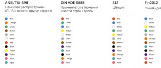
Foreign products received a different designation system. When choosing an analogue, use special correspondence tables. For the rest, the import base differs little from the domestic one. Marking is carried out according to JEDEC standards (USA), European system (PRO ELECTRON). Colorful color code decoding tables are massively provided by online sources.
Color coding
New notation system
The new diode marking system is more advanced. It consists of four elements.
The first element (letter or number) indicates the source semiconductor material from which the diode is made: G or 1 - germanium * K or 2 - silicon, A or 3 - gallium arsenide, I or 4 - indium phosphide.
The second element is a letter indicating the class or group of the diode.
The third element is a number that determines the purpose or electrical properties of the diode.
The fourth element indicates the serial number of the technological development of the diode and is designated from A to Z.
- diode KD202A stands for: K - material, silicon, D - rectifier diode, 202 - purpose and development number, A - variety;
- 2C920 - high power silicon zener diode of type A variety;
- AI301B is a gallium arsenide tunnel diode of the switching type B.
Sometimes there are diodes designated according to outdated systems: DG-Ts21, D7A, D226B, D18. D7 diodes differ from DG-Ts diodes in their all-metal housing design, as a result of which they operate more reliably in a humid atmosphere.
Germanium diodes type DG-Ts21. DG-Ts27 and D7A diodes similar in characteristics. D7Zh is usually used in rectifiers to power radio equipment from an alternating current network.
The diode designation does not always include some technical data, so you need to look for them in reference books on semiconductor devices.
One of the exceptions is the designation for some diodes with the letters KS or a number instead of K (for example, 2C) - silicon zener diodes and stabilistors.
After these designations there are three digits, if these are the first digits: 1 or 4, then taking the last two digits and dividing them by 10 we get the stabilization voltage Ust.
- KS107A - stabistor, Ust = 0.7 V,
- 2S133A - zener diode, Ust = 3.3 V.
If the first digit is 2 or 5, then the last two digits show Ust, for example:
- KS 213B - Ust = 13 V,
- 2C 291A - Ust = 91 V.
If the number is 6, then you need to add 100 V to the last two digits, for example: KS 680A - Ust = 180 V.
Japanese JIS system
This system consists of symbols and contains five elements. The first digit corresponds to the type of semiconductor device: 0 – photodiode or phototransistor; 1 – diode; 2 – transistor. The second element is the letter S, it is placed on all elements. The following letter corresponds to the type of transistor: A – high-frequency PNP; B – low-frequency PNP; C—high-frequency NPN; D—low-frequency NPN; N – single-junction; J - field with N-channel; K - field with P-channel. This is followed by the product serial number (10 – 9999). The last, fifth, element is a modification of the device (often it may be missing). Sometimes a sixth character is also applied - this is an additional index (letters N, M or S), indicating the requirement of compliance with special standards. In the Japanese system, color coding of transistors is not used.
SMD marking of electrical elements
The principle of marking is the encrypted transmission of information about the dimensions and electrical parameters of the chip. There is a conditional division according to the number of pins and the size of the element housing:
| Number of pins | Case marking in ascending order of size | Short description |
| Two-pin | SOD (for example, SOD128, SOD323, etc.) or WLCSP2 | Passive chips of cylindrical or square shape, tantalum capacitors, diodes |
| Three-pin | DPAK, D2PAK, D3PAK | The author of this case is Motorola. All elements have the same shape, but different sizes. Used for semiconductor elements that produce thermal energy |
| Four-pin and more | WLCSP(N) (N indicates the number of pins), SOT, SOIC, SSOP, CLCC, LQFP, DFN, DIP / DIL, Flat Pack, TSOP, ZIP | The contacts of these chips are located on two opposite sides of the case |
| Elements with more than four contacts | LCC, PLCC, QFN, QFP, QUIP | Pins are located on all four sides of the housing |
| The pins are arranged in a lattice pattern | BGA, uBGA | Microcircuits intended for soldering using special paste |
| Leadless elements | μBGA, LFBGA | Equipped with contact strips or solder drops only |
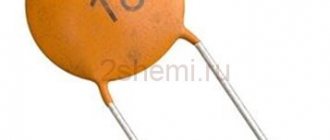
Chip capacitors
There are two main types of capacitors - electrolytic (the body is cylindrical) and ceramic or tantalum (the body is shaped like a parallelepiped). Electrolyte markings always contain capacitance and voltage values, but ceramic samples do not. The minus (cathode) of the electrolytes is indicated by a strip located on the upper side of the housing.
Marking of SMD resistors
The marking is represented by several characters - numbers and letters. The first two digits indicate the denomination, and the third (and fourth) indicate the order, or the number of zeros. For example, the number 322 means 3200 ohms or 3.2 kohms. Sometimes the R separator is used, acting as a comma. So, the designation 3R2 means 3.2 kOhm. Or 0R32 - 0.32 kOhm.
There are special resistors that act as fuses or jumpers. They have a zero resistance rating.
The dimensions of SMD devices are standardized and associated with markings. Thus, chips of diodes, resistors or capacitors of size 0805 have parameters of 0.6 × 0.8 × 0.23 inches (length-width-height).
SMD inductance
The shape and dimensions of the housings of the chokes and inductors have the same values as those of resistors or capacitors. The designation consists of 4 digits. The first two are the length, the others are the width of the chip, expressed in tenths of an inch. For example, the throttle marking 0805 means that its length is 0.08 and its width is 0.05 inches.
SMD diodes and transistors
Diode chips can be made in the form of a barrel or parallelepiped (briquette). All sizes fully correspond to the parameters of the resistors, which simplifies the development of printed circuit boards. Given the specific operation of diodes, for which polarity must be observed, there is a strip on or near the negative terminal. It designates the cathode, which helps avoid installation errors.
On the surface of the chip there can only be a code that does not provide complete information about the parameters of the part. Therefore, there are special information arrays - datasheets, which contain information about all the parameters and capabilities of the elements. If you need complete data on the properties that transistors have, the datasheet makes it possible to obtain detailed information.
Two types of housings are used:
In addition to transistors, diode assemblies used in rectifiers and drivers can be produced in this format.
SMD transistor code table
| Designation on the body | Transistor type |
| "15" on the SOT-23 case | MMBT3960 (Datasheet "Motorola") |
| "1A" on the SOT-23 case | BC846A (Datasheet "Taitron") |
| "1B" on the SOT-23 case | BC846B (Datasheet "Taitron") |
| "1C" on the SOT-23 case | MMBTA20LT (Datasheet "Motorola") |
| "1D" on the SOT-23 case | BC846 (Datasheet "NXP") |
| "1E" on the SOT-23 case | BC847A (Datasheet "Taitron") |
| "1F" on the SOT-23 case | BC847B (Datasheet "Taitron") |
| "1G" on the SOT-23 case | BC847C (Datasheet "Taitron") |
| "1H" on the SOT-23 case | BC847 (Datasheet "NXP") |
| "1N" on the SOT-416 case | BC847T (Datasheet "NXP") |
| "1J" on the SOT-23 case | BC848A (Datasheet "Taitron") |
| "1K" on the SOT-23 case | BC848B (Datasheet "Taitron") |
| "1L" on the SOT-23 case | BC848C (Datasheet "Taitron") |
| "1M" on the SOT-416 case | BC846T (Datasheet "NXP") |
| "1M" on the SOT-323 case | BC848W (Datasheet "NXP") |
| "1M" on the SOT-23 case | MMBTA13 (Datasheet "Motorola") |
| "1N" on the SOT-23 case | MMBTA414 (Datasheet "Motorola") |
| "1V" on the SOT-23 case | MMBT6427 (Datasheet "Motorola") |
| "1P" on the SOT-23 case | FMMT2222A,KST2222A,MMBT2222A. |
| "1T" on the SOT-23 case | MMBT3960A (Datasheet “Motorola”) |
| "1Y" on the SOT-23 case | MMBT3903 (Datasheet “Samsung”) |
| "2A" on the SOT-23 case | FMMBT3906,KST3906,MMBT3906 |
| "2B" on the SOT-23 case | BC849B (Datasheet "GS") |
| "2C" on the SOT-23 case | BC849C (Datasheet "GS") |
| "2E" on the SOT-23 case | FMMTA93, KST93 |
| "2F" on the SOT-23 case | FMMT2907A,KST2907A,MMBT2907AT |
| “2G” on the SOT-23 case | FMMTA56,KST56 |
| "2H" on the SOT-23 case | MMBTA55(Datasheet "Taitron") |
| "2J" on the SOT-23 case | MMBT3640(Datasheet “Fairchild”) |
| "2K" on the SOT-23 case | FMMT4402(Datasheet “Zetex”) |
| "2M" on the SOT-23 case | MMBT404(Datasheet “Motorola”) |
| "2N" on the SOT-23 case | MMBT404A(Datasheet “Motorola”) |
| "2T" on the SOT-23 case | KST4403,MMBT4403 |
| "2V" on the SOT-23 case | MMBTA64(Datasheet "Motorola") |
| "2U" on the SOT-23 case | MMBTA63(Datasheet "Motorola") |
| "2X" on the SOT-23 case | MMBT4401,KST4401 |
| "3A" on the SOT-23 case | MMBTH24(Datasheet “Motorola”) |
| "3B" on the SOT-23 case | MMBT918(Datasheet “Motorola”) |
| "3D" on the SOT-23 case | MMBTH81(Datasheet “Motorola”) |
| "3E" on the SOT-23 case | MMBTH10(Datasheet “Motorola”) |
| "3F" on the SOT-23 case | MMBT6543(Datasheet “Motorola”) |
| "3J-" on the SOT-143B case | BCV62A(Datasheet "NXP") |
| “3K-” on the SOT-23 case | BC858B(Datasheet "NXP") |
| “3L-” on the SOT-143B case | BCV62C(Datasheet "NXP") |
| "3S" on the SOT-23 case | MMBT5551(Datasheet “Fairchild”) |
| "4As" on the SOT-23 case | BC859A(Datasheet "Siemens") |
| "4Bs" on the SOT-23 case | BC859B(Datasheet "Siemens") |
| "4Cs" on the SOT-23 case | BC859C(Datasheet "Siemens") |
| "4J" on the SOT-23 case | FMMT38A(Datasheet “Zetex S.”) |
| "449" on the SOT-23 case | FMMT449(Datasheet "Diodes Inc.") |
| "489" on the SOT-23 case | FMMT489(Datasheet "Diodes Inc.") |
| "491" on the SOT-23 case | FMMT491(Datasheet "Diodes Inc.") |
| "493" on the SOT-23 case | FMMT493(Datasheet "Diodes Inc.") |
| "5A" on the SOT-23 case | BC807-16(Datasheet "General Sem.") |
| "5B" on the SOT-23 case | BC807-25(Datasheet "General Sem.") |
| "5C" on the SOT-23 case | BC807-40(Datasheet "General Sem.") |
| "5E" on the SOT-23 case | BC808-16(Datasheet "General Sem.") |
| "5F" on the SOT-23 case | BC808-25(Datasheet "General Sem.") |
| "5G" on the SOT-23 case | BC808-40(Datasheet "General Sem.") |
| "5J" on the SOT-23 body | FMMT38B(Datasheet “Zetex S.”) |
| "549" on the SOT-23 case | FMMT549(Datasheet "Fairchild") |
| "589" on the SOT-23 case | FMMT589(Datasheet "Fairchild") |
| "591" on the SOT-23 case | FMMT591(Datasheet “Fairchild”) |
| "593" on the SOT-23 case | FMMT593(Datasheet “Fairchild”) |
| “6A-“,”6Ap”,”6At” on the SOT-23 body | BC817-16(Datasheet "NXP") |
| “6B-“,”6Bp”,”6Bt” on the SOT-23 case | BC817-25(Datasheet "NXP") |
| “6C-“,”6Cp”,”6Ct” on the SOT-23 case | BC817-40(Datasheet "NXP") |
| "6E-", "6Et", "6Et" on the SOT-23 case | BC818-16(Datasheet "NXP") |
| "6F-", "6Ft", "6Ft" on the SOT-23 case | BC818-25(Datasheet "NXP") |
| “6G-“,”6Gt”,”6Gt” on the SOT-23 case | BC818-40(Datasheet "NXP") |
| "7J" on the SOT-23 case | FMMT38C(Datasheet “Zetex S.”) |
| "9EA" on the SOT-23 case | BC860A(Datasheet "Fairchild") |
| "9EB" on the SOT-23 case | BC860B(Datasheet "Fairchild") |
| "9EC" on SOT-23 case | BC860C(Datasheet "Fairchild") |
| "AA" on the SOT-523F case | 2N7002T(Datasheet “Fairchild”) |
| "AA" on the SOT-23 case | BCW60A(Datasheet “Diotec Sem.”) |
| "AB" on SOT-23 body | BCW60B(Datasheet “Diotec Sem.”) |
| "AC" on the SOT-23 case | BCW60C(Datasheet “Diotec Sem.”) |
| "AD" on the SOT-23 case | BCW60D(Datasheet “Diotec Sem.”) |
| "AE" on the SOT-89 case | BCX52(Datasheet "NXP") |
| "AG" on the SOT-23 case | BCX70G(Datasheet “Central Sem.Corp.”) |
| "AH" on the SOT-23 body | BCX70H(Datasheet “Central Sem.Corp.”) |
| "AJ" on the SOT-23 body | BCX70J(Datasheet “Central Sem.Corp.”) |
| "AK" on the SOT-23 case | BCX70K(Datasheet “Central Sem.Corp.”) |
| "AL" on the SOT-89 case | BCX53-16(Datasheet “Zetex”) |
| "AM" on the SOT-89 case | BCX52-16(Datasheet “Zetex”) |
| "AS1" on the SOT-89 case | BST50(Datasheet "Philips") |
| "B2" on the SOT-23 case | BSV52(Datasheet "Diotec Sem.") |
| "BA" on the SOT-23 case | BCW61A(Datasheet "Fairchild") |
| "BA" on the SOT-23 case | 2SA1015LT1(Datasheet “Tip”) |
| "BA" on the SOT-23 case | 2SA1015(Datasheet “BL Galaxy El.”) |
| "BB" on SOT-23 case | BCW61B(Datasheet "Fairchild") |
| "BC" on the SOT-23 case | BCW61C(Datasheet "Fairchild") |
| "BD" on the SOT-23 case | BCW61D(Datasheet "Fairchild") |
| "BE" on the SOT-89 case | BCX55(Datasheet » BL Galaxy El.) |
| "BG" on the SOT-89 case | BCX55-10(Datasheet » BL Galaxy El.) |
| "BH" on the SOT-89 case | BCX56(Datasheet "BL Galaxy El.") |
| "BJ" on the SOT-23 case | BCX71J(Datasheet “Diotec Sem.”) |
| "BK" on the SOT-23 case | BCX71K(Datasheet “Diotec Sem.”) |
| "BH" on the SOT-23 case | BCX71H(Datasheet “Diotec Sem.”) |
| "BG" on the SOT-23 case | BCX71G(Datasheet “Diotec Sem.”) |
| "BR2" on SOT-89 case | BSR31(Datasheet "Zetex") |
| "C1" on the SOT-23 case | BCW29(Datasheet "Diotec Sem.") |
| "C2" on the SOT-23 case | BCW30(Datasheet "Diotec Sem.") |
| "C5" on the SOT-23 case | MMBA811C5(Datasheet “Samsung Sem.”) |
| "C6" on the SOT-23 case | MMBA811C6(Datasheet “Samsung Sem.”) |
| "C7" on the SOT-23 case | BCF29(Datasheet "Diotec Sem.") |
| "C8" on the SOT-23 case | BCF30(Datasheet "Diotec Sem.") |
| "CEs" on the SOT-23 case | BSS79B(Datasheet "Siemens") |
| "CEC" on the SOT-89 case | BC869(Datasheet "Philips") |
| "CFs" on the SOT-23 body | BSS79C(Datasheet "Siemens") |
| "CHs" on the SOT-23 case | BSS80B(Datasheet "Infenion") |
| "CJs" on the SOT-23 case | BSS80C(Datasheet "Infenion") |
| "CMs" on the SOT-23 case | BSS82C(Datasheet "Infenion") |
| "CLs" on the SOT-23 case | BSS82B(Datasheet "Infenion") |
| "D1" on the SOT-23 case | BCW31(Datasheet "KEC") |
| "D2" on the SOT-23 case | BCW32(Datasheet "KEC") |
| "D3" on the SOT-23 case | BCW33(Datasheet "KEC") |
| D6″ on SOT-23 body | MMBC1622D6(Datasheet “Samsung Sem.”) |
| “D7t”, “D7p” on the SOT-23 case | BCF32(Datasheet "NXP Sem.") |
| "D7" on the SOT-23 case | BCF32(Datasheet "Diotec Sem.") |
| "D8" on the SOT-23 case | BCF33(Datasheet "Diotec Sem.") |
| "DA" on the SOT-23 case | BCW67A(Datasheet "Central Sem. Corp.") |
| "DB" on the SOT-23 case | BCW67B(Datasheet "Central Sem. Corp.") |
| "DC" on the SOT-23 case | BCW67C(Datasheet "Central Sem. Corp.") |
| "DF" on the SOT-23 case | BCW67F(Datasheet "Central Sem. Corp.") |
| "DG" on the SOT-23 case | BCW67G(Datasheet "Central Sem. Corp.") |
| "DH" on the SOT-23 case | BCW67H(Datasheet "Central Sem. Corp.") |
| "E2p" on the SOT-23 case | BFS17A(Datasheet "Philips") |
| "EA" on the SOT-23 case | BCW65A(Datasheet "Central Sem. Corp.") |
| "EB" on the SOT-23 case | BCW65B(Datasheet "Central Sem. Corp.") |
| "EC" on the SOT-23 case | BCW65C(Datasheet "Central Sem. Corp.") |
| "EF" on the SOT-23 case | BCW65F(Datasheet "Central Sem. Corp.") |
| "EG" on the SOT-23 case | BCW65G(Datasheet "Central Sem. Corp.") |
| "EH" on the SOT-23 case | BCW65H(Datasheet "Central Sem. Corp.") |
| "F1" on the SOT-23 case | MMBC1009F1(Datasheet “Samsung Sem.”) |
| "F3" on the SOT-23 case | MMBC1009F3(Datasheet “Samsung Sem.”) |
| "FA" on the SOT-89 case | BFQ17(Datasheet "Philips") |
| “FDp”,”FDt”,”FDW” on the SOT-23 case | BCV26(Datasheet “Philips(NXP)”) |
| “FEp”,”FEt”,”FEW” on the SOT-23 case | BCV46(Datasheet “Philips(NXP)”) |
| “FFp”,”FFt”,”FFW” on the SOT-23 case | BCV27(Datasheet “Philips(NXP)”) |
| "FGp","FGt","FGW" on SOT-23 | BCV47(Datasheet “Philips(NXP)”) |
| "GFs" on the SOT-23 case | BFR92P(Datasheet “Infenion”) |
| “H1p”,”H1t”,”H1W” on the SOT-23 case | BCV69(Datasheet “Philips(NXP)”) |
| “H2p”,”H2t”,”H2W” on the SOT-23 case | BCV70(Datasheet “Philips(NXP)”) |
| “H3p”,”H3t” on the SOT-23 case | BCV89(Datasheet “Philips(NXP)”) |
| "H7p" on the SOT-23 case | BCF70 |
| "K1" on the SOT-23 case | BCW71(Datasheet “Samsung Sem.”) |
| "K2" on the SOT-23 case | BCW72(Datasheet “Samsung Sem.”) |
| "K3p" on the SOT-23 case | BCW81(Datasheet “Philips(NXP)”) |
| “K1p”,”K1t” on the SOT-23 case | BCW71(Datasheet “Philips(NXP)”) |
| “K2p”,”K2t” on the SOT-23 case | BCW72(Datasheet “Philips(NXP)”) |
| “K7p”,”K7t” on the SOT-23 case | BCV71(Datasheet “Philips(NXP)”) |
| “K8p”,”K8t” on the SOT-23 case | BCV72(Datasheet “Philips(NXP)”) |
| "K9p" on the SOT-23 case | BCF81(Datasheet » Guangdong Kexin Ind.Co.Ltd") |
| "L1" on the SOT-23 case | BSS65 |
| "L2" on the SOT-23 case | BSS69(Datasheet "Zetex Sem.") |
| "L3" on the SOT-23 case | BSS70(Datasheet "Zetex Sem.") |
| "L4" on the SOT-23 case | 2SC1623L4(Datasheet “BL Galaxy El.”) |
| "L5" on the SOT-23 case | BSS65R |
| "L6" on the SOT-23 case | BSS69R(Datasheet "Zetex Sem.") |
| "L7" on the SOT-23 case | BSS70R(Datasheet “Zetex Sem.”) |
| "M3" on SOT-23 case | MMBA812M3(Datasheet “Samsung Sem.”) |
| "M4" on SOT-23 case | MMBA812M4(Datasheet “Samsung Sem.”) |
| "M5" on SOT-23 case | MMBA812M5(Datasheet “Samsung Sem.”) |
| "M6" on SOT-23 case | MMBA812M6(Datasheet “Samsung Sem.”) |
| "M6P" on SOT-23 case | BSR58(Datasheet "Philips(NXP)") |
| "M7" on SOT-23 case | MMBA812M7(Datasheet “Samsung Sem.”) |
| "P1" on the SOT-23 case | BFR92(Datasheet “Vishay Telefunken”) |
| "P2" on the SOT-23 case | BFR92A(Datasheet “Vishay Telefunken”) |
| "P4" on the SOT-23 case | BFR92R(Datasheet “Vishay Telefunken”) |
| "P5" on the SOT-23 case | FMMT2369A(Datasheet “Zetex Sem.”) |
| "Q2" on the SOT-23 case | MMBC1321Q2(Datasheet “Motorola Sc.”) |
| "Q3" on the SOT-23 case | MMBC1321Q3(Datasheet “Motorola Sc.”) |
| "Q4" on the SOT-23 case | MMBC1321Q4(Datasheet “Motorola Sc.”) |
| "Q5" on the SOT-23 case | MMBC1321Q5(Datasheet “Motorola Sc.”) |
| "R1p" on the SOT-23 case | BFR93(Datasheet “Philips(NXP)”) |
| "R2p" on the SOT-23 case | BFR93A(Datasheet “Philips(NXP)”) |
| “s1A” on SOT-23, SOT-363 cases | SMBT3904(Datasheet “Infineon”) |
| "s1D" on the SOT-23 case | SMBTA42(Datasheet "Infineon") |
| "S2" on the SOT-23 case | MMBA813S2(Datasheet “Motorola Sc.”) |
| "s2A" on the SOT-23 case | SMBT3906(Datasheet “Infineon”) |
| "s2D" on the SOT-23 case | SMBTA92(Datasheet “Siemens Sem.”) |
| "s2F" on the SOT-23 case | SMBT2907A(Datasheet “Infineon”) |
| "S3" on the SOT-23 case | MMBA813S3(Datasheet “Motorola Sc.”) |
| "S4" on the SOT-23 case | MMBA813S4(Datasheet “Motorola Sc.”) |
| "T1" on the SOT-23 case | BCX17(Datasheet “Philips(NXP)”) |
| "T2" on the SOT-23 case | BCX18(Datasheet “Philips(NXP)”) |
| "T7" on SOT-23 case | BSR15(Datasheet "Diotec Sem.") |
| "T8" on SOT-23 case | BSR16 (Datasheet "Diotec Sem.") |
| “U1p”, “U1t”, “U1W” on the SOT-23 case | BCX19 (Datasheet “Philips(NXP)”) |
| "U2" on the SOT-23 case | BCX20 (Datasheet "Diotec Sem.") |
| “U7p”, “U7t”, “U7W” on the SOT-23 case | BSR13 (Datasheet “Philips(NXP)”) |
| “U8p”, “U8t”, “U8W” on the SOT-23 case | BSR14 (Datasheet "Philips(NXP)") |
| "U92" on SOT-23 case | BSR17A (Philips Datasheet) |
| "Z2V" on the SOT-23 case | FMMTA64 (Datasheet “Zetex Sem.”) |
| "ZD" on the SOT-23 case | MMBT4125 (Datasheet “Samsung Sem.”) |
Marking of imported diodes
Currently, foreign-made SMD diodes are widely used. The design of the elements is made in the form of a board, on the surface of which a chip is fixed. The dimensions of the product are too small to allow marking to be applied to it. On larger elements, designations are present in full or abbreviated versions.
In electronics, SMD diodes make up about 80% of all products of this type used. Such a variety of details makes you pay more attention to the designations. Sometimes they may not coincide with the declared technical characteristics, so it is advisable to carry out additional checks of questionable elements if they are planned for use in complex and precise circuits. It should be borne in mind that the markings of diodes of this type may be different on completely identical cases. Sometimes there are only alphabetic symbols, without any numbers. In this regard, it is recommended to use tables with diode sizes from different manufacturers.
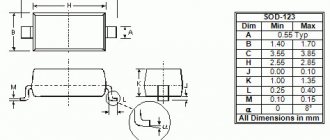
For SMD diodes, the SOD123 package type is most often used. A colored stripe or embossing may be applied to one of the ends, which indicates a cathode with negative polarity to open the pn junction. The only inscription corresponds to the designation of the case.
The type of housing does not play a decisive role when using a diode. One of the main characteristics is the dissipation of some amount of heat from the surface of the element. In addition, the values of the operating and reverse voltages, the maximum permissible current through the pn junction, power dissipation and other parameters are taken into account. All this data is indicated in reference books, and marking only speeds up the search for the desired element.
It is not always possible to determine the manufacturer by the appearance of the case. To find the desired product, there are special search engines into which you need to enter numbers and letters in a certain sequence. In some cases, diode assemblies do not carry any information at all, so in such cases only a reference book can help. Such simplifications, which make the diode designation very short, are explained by the extremely limited space for marking. When using screen or laser printing, it is possible to fit 8 characters per 4 mm2.
It is also worth considering the fact that the same alphanumeric code can denote completely different elements. In such cases, the entire electrical circuit is analyzed.
Sometimes the labeling indicates the release date and batch number. Such marks are applied to be able to track more modern modifications of products. The corresponding corrective documentation with number and date is issued. This allows you to more accurately establish the technical characteristics of elements when assembling the most critical circuits. By using old parts for new drawings, you may not get the expected result; in most cases, the finished product simply refuses to work.
Types of recording
Transistor manufacturers use two main types of encryption: color coding and code marking. However, neither one nor the other has uniform standards. Each plant that produces semiconductor devices (transistors, diodes, zener diodes, etc.) adopts its own code and color designations. You can find transistors of the same group and type, manufactured by different factories, and they will be labeled differently. Or vice versa: the elements will be different, but the designations on them will be identical. In such cases, they can be distinguished only by additional characteristics. For example, by the length of the emitter and collector leads or by the color of the opposite (or end) surface. The markings of field-effect transistors are no different from the marks on other devices. The situation is the same with foreign-made semiconductor elements: each manufacturer uses its own types of designations.
What is this element of electrical circuits?
Before we begin to consider the question of what color markings exist for such elements, we need to understand what it is all about.
Volt-ampere characteristic of a zener diode
A zener diode is a semiconductor diode, which is designed to stabilize the DC voltage across the load in an electrical circuit. Most often, such a diode is used to stabilize voltage in various power supplies. This diode (smd) has a section with a reverse branch of the current-voltage characteristic, which is observed in the region of electrical breakdown.
Having such an area, the zener diode in a situation where the parameter of the current flowing through the diode changes from IST.MIN to IST.MAX, practically no changes in the voltage indicator are observed. This effect is used to stabilize voltage. In a situation where the RH load is connected in parallel to the SMD, then the diode voltage will remain constant, and within the specified limits of change in the current flowing through the zener diode.
In addition to SMD, there are also zeners, which are turned on when switched on directly. They are used in situations where there is a need to stabilize the voltage in a certain range. A conventional diode can be used when it is necessary to stabilize the voltage in the range from 0.3 to 0.5 V. The region of their forward bias is observed when the voltage drops to 0.7 - 2v. Moreover, it practically does not depend on the current strength. In their work, stabistors use the direct branch of the current-voltage characteristic. They should also be turned on when connected directly. Although this will not be the best solution, since a zener diode in such a situation will still be more effective. Stabistors, like SMD, are often made from silicon. Zener diodes are labeled according to their main characteristics. This marking looks like this:
- UST. This marking indicates the rated voltage for stabilization;
- ΔUST. Indicates the deviation of the voltage indicator of the rated stabilization voltage;
- IST. Indicates the current that flows through the diode at the rated stabilization voltage;
- IST.MIN - the minimum value of the current that flows through the zener diode. At this value, such an SMD diode will have a voltage in the range UST ± ΔUST;
- IST.MAX. Indicates the maximum permissible amount of current that can flow through the zener diode.
This marking is important when choosing an element for a specific electrical circuit.
Schottky diode application
These electronic elements presented above can be found in our world almost everywhere: in computers, stabilizers, household appliances, radio broadcasting, television, power supplies, solar panels, transistors and in many other devices from all spheres of life.
In all cases, it increases efficiency and performance, reduces the number of losses in voltage dynamics, restores the reverse current resistance, absorbs the radiation of alpha, beta and gamma charges, allows you to work for a long time without breakdowns, and maintains the current in the voltage of the electrical circuit.
Diodes and zener diodes in SMD housing
As for diodes, they are also available in both cylindrical and polyhedron-shaped cases. The typical dimensions of these components are set identically to inductive coils, resistors and capacitors.
| Diodes, Zener diodes, capacitors, resistors | |||||
| Type of shell | L* (mm) | D* (mm) | F* (mm) | S* (mm) | Note |
| DO-213AA (SOD80) | 3.5 | 1.65 | 048 | 0.03 | JEDEC |
| DO-213AB (MELF) | 5.0 | 2.52 | 0.48 | 0.03 | JEDEC |
| DO-213AC | 3.45 | 1.4 | 0.42 | — | JEDEC |
| ERD03LL | 1.6 | 1.0 | 0.2 | 0.05 | PANASONIC |
| ER021L | 2.0 | 1.25 | 0.3 | 0.07 | PANASONIC |
| ERSM | 5.9 | 2.2 | 0.6 | 0.15 | PANASONIC, GOST R1-11 |
| MELF | 5.0 | 2.5 | 0.5 | 0.1 | CENTS |
| SOD80 (miniMELF) | 3.5 | 1.6 | 0.3 | 0.075 | PHILIPS |
| SOD80C | 3.6 | 1.52 | 0.3 | 0.075 | PHILIPS |
| SOD87 | 3.5 | 2.05 | 0.3 | 0.075 | PHILIPS |
Standard sizes of SMD components
Chip components of the same denomination may have different dimensions. The dimensions of an SMD component are determined by its “standard size”. For example, chip resistors have standard sizes from “0201” to “2512”. These four digits encode the width and length of the chip resistor in inches. In the tables below you can see the standard sizes in millimeters.
smd resistors
| Square Chip Resistors and Ceramic Capacitors | |||||
| Standard size | L, mm (inch) | W, mm (inch) | H, mm (inch) | A, mm | W |
| 0201 | 0.6 (0.02) | 0.3 (0.01) | 0.23 (0.01) | 0.13 | 1/20 |
| 0402 | 1.0 (0.04) | 0.5 (0.01) | 0.35 (0.014) | 0.25 | 1/16 |
| 0603 | 1.6 (0.06) | 0.8 (0.03) | 0.45 (0.018) | 0.3 | 1/10 |
| 0805 | 2.0 (0.08) | 1.2 (0.05) | 0.4 (0.018) | 0.4 | 1/8 |
| 1206 | 3.2 (0.12) | 1.6 (0.06) | 0.5 (0.022) | 0.5 | 1/4 |
| 1210 | 5.0 (0.12) | 2.5 (0.10) | 0.55 (0.022) | 0.5 | 1/2 |
| 1218 | 5.0 (0.12) | 2.5 (0.18) | 0.55 (0.022) | 0.5 | 1 |
| 2010 | 5.0 (0.20) | 2.5 (0.10) | 0.55 (0.024) | 0.5 | 3/4 |
| 2512 | 6.35 (0.25) | 3.2 (0.12) | 0.55 (0.024) | 0.5 | 1 |
| Cylindrical chip resistors and diodes | |||||
| Standard size | Ø, mm (inch) | L, mm (inch) | W | ||
| 0102 | 1.1 (0.01) | 2.2 (0.02) | 1/4 | ||
| 0204 | 1.4 (0.02) | 3.6 (0.04) | 1/2 | ||
| 0207 | 2.2 (0.02) | 5.8 (0.07) | 1 | ||
smd capacitors
Ceramic chip capacitors are the same size as chip resistors, but tantalum chip capacitors have their own size system:
| Tantalum capacitors | |||||
| Standard size | L, mm (inch) | W, mm (inch) | T, mm (inch) | B, mm | A, mm |
| A | 3.2 (0.126) | 1.6 (0.063) | 1.6 (0.063) | 1.2 | 0.8 |
| B | 3.5 (0.138) | 2.8 (0.110) | 1.9 (0.075) | 2.2 | 0.8 |
| C | 6.0 (0.236) | 3.2 (0.126) | 2.5 (0.098) | 2.2 | 1.3 |
| D | 7.3 (0.287) | 4.3 (0.170) | 2.8 (0.110) | 2.4 | 1.3 |
| E | 7.3 (0.287) | 4.3 (0.170) | 4.0 (0.158) | 2.4 | 1.2 |
smd inductors and chokes
Inductors are found in many types of housings, but the housings are subject to the same size law. This makes automatic installation easier. And it makes it easier for us, radio amateurs, to navigate.
All kinds of coils, chokes and transformers are called “winding products”. Usually we wind them ourselves, but sometimes you can buy ready-made products. Moreover, if SMD options are required, which come with many bonuses: magnetic shielding of the housing, compactness, closed or open housing, high quality factor, electromagnetic shielding, wide range of operating temperatures.
It is better to select the required coil according to catalogs and the required standard size. Standard sizes, as for chip resistors, are specified using a four-number code (0805). In this case, “08” indicates the length, and “05” the width in inches. The actual size of such an SMD component will be 0.08x0.05 inches.
Marking of imported diodes
Currently, foreign-made SMD diodes are widely used. The design of the elements is made in the form of a board, on the surface of which a chip is fixed. The dimensions of the product are too small to allow marking to be applied to it. On larger elements, designations are present in full or abbreviated versions. In electronics, SMD diodes make up about 80% of all products of this type used. Such a variety of details makes you pay more attention to the designations. Sometimes they may not coincide with the declared technical characteristics, so it is advisable to carry out additional checks of questionable elements if they are planned for use in complex and precise circuits. It should be borne in mind that the markings of diodes of this type may be different on completely identical cases. Sometimes there are only alphabetic symbols, without any numbers. In this regard, it is recommended to use tables with diode sizes from different manufacturers.
For SMD diodes, the SOD123 package type is most often used. A colored stripe or embossing may be applied to one of the ends, which indicates a cathode with negative polarity to open the pn junction. The only inscription corresponds to the designation of the body. The type of housing does not play a decisive role when using a diode. One of the main characteristics is the dissipation of some amount of heat from the surface of the element. In addition, the values of the operating and reverse voltages, the maximum permissible current through the pn junction, power dissipation and other parameters are taken into account. All this data is indicated in reference books, and marking only speeds up the search for the desired element.
It is not always possible to determine the manufacturer by the appearance of the case. To find the desired product, there are special search engines into which you need to enter numbers and letters in a certain sequence. In some cases, diode assemblies do not carry any information at all, so in such cases only a reference book can help. Such simplifications, which make the diode designation very short, are explained by the extremely limited space for marking. When using screen or laser printing, it is possible to fit 8 characters per 4 mm2. It is also worth considering the fact that the same alphanumeric code can denote completely different elements. In such cases, the entire electrical circuit is analyzed.
Sometimes the labeling indicates the release date and batch number. Such marks are applied to be able to track more modern modifications of products. The corresponding corrective documentation with number and date is issued. This allows you to more accurately establish the technical characteristics of elements when assembling the most critical circuits. By using old parts for new drawings, you may not get the expected result; in most cases, the finished product simply refuses to work.
Soldering chip components
At home, chip components can only be soldered up to a certain size; size 0805 is considered more or less comfortable for manual installation. Smaller components are soldered using a stove. At the same time, for high-quality soldering at home, a whole range of measures should be observed.
Modern printed circuit boards look different from their predecessors. The familiar parts with legs inserted into holes have practically disappeared. They were replaced by very tiny components soldered on top of the board to specially created contact pads. They are called SMD (Surface Mounted Device, or surface-mounted device).
Such parts are much more convenient - the whole and very precise operation of drilling holes in the manufacture of the board is eliminated, and compactness is achieved. At the same time, their miniature size does not allow them to be labeled with a detailed and familiar name. The marking of SMD diodes is made in the form of codes, which need to be discussed in more detail.
Main conclusions
Knowledge of the markings of SMD diodes and other components will help when performing repair work, identifying analogues or options for replacing parts. To obtain detailed information about the parameters of elements, you must use the following sources:
- directory of SMD component codes;
- datasheet (mainly for transistors);
- deciphering the code for resistors or chokes.
The number of SMD diodes and other parts is large. Many manufacturers develop their own marking system, which is in no way correlated with other designations, which introduces significant confusion into the process of identifying and replacing problematic elements. Therefore, it is important to have reference books and complete blocks of information on the parameters of diodes or other parts from different companies on hand. State your methods for identifying chips in the comments.
Previous
LEDs Changing the LED in a flashlight with your own hands
Next
LEDsScheme and features of connecting LED backlight to a computer
Nuances
In addition to such diode designations, some graphical indicators are also used. Thanks to them, you can solve the problem and understand how high the operating point of the device is. Sometimes the diodes are marked with information about what production technique was chosen, what housing material is available, and the weight of the device. In principle, such information will be useful to those who create equipment; amateurs do not need such data.
It should be noted that imported manufacturers work according to a different scheme. The marking of a diode of this type will be quite simple; its meaning can be found in a special table. That is why analogues will be very easy to find.
Miniaturization
With the development of microelectronics, special microcircuits and single-chip microprocessors began to be widely used. All this does not exclude the use of hanging elements. However, if radioelements of conventional sizes are used for this purpose, this will negate the whole idea of miniaturization as a whole. Therefore, open-frame elements were developed - SMD components, which are 10 or more times smaller than conventional parts. The current-voltage characteristics of such components are no different from the current-voltage characteristics of conventional devices, and their reduced dimensions make it possible to use such spare parts in various microassemblies.
The operating principle of an smd component is also no different from its large counterpart, and if, for example, we consider the current-voltage characteristic of a diode, then it will be equally suitable for semiconductors of any size. The current range is from 1 to 10 amperes. The markings on the case often consist of a digital code, the decoding of which is given in special tables. They can be tested for suitability using a tester, just like their larger counterparts.
Marking of year and month of manufacture
In accordance with GOST 25486-82, two letters or a letter and a number are used to indicate the date. The first character corresponds to the year, and the second to the month. This type of coding is used not only for transistors, but also for other domestic semiconductor elements. On foreign instruments, the date is indicated by four digits, the first two of which correspond to the year, and the last - the week number. Let's consider what the code marking of transistors means, corresponding to the date of manufacture. Year of issue/symbol: 1986 – U, 1987 – V, 1988 – W, 1989 – X, 1990 – A, 1991 – B, 1992 – C, 1993 – D, 1994 – E, 1995 – F, 1996 – H, 1997 – I, 1998 – K, 1999 – L, 2000 – M, etc. Month of issue: the first nine months correspond to the numbers from 1 to 9 (January – 1, February – 2), and the last ones correspond to the initial letters of the word: October – Oh, November - N, December - D.