A vacuum diode is a device that works by controlling the heating intensity of the positive and negative poles of the device. When an electric current is applied, the input of the device heats up, after which the effect of electrons leaving the metal appears. If an electric current with a negative voltage is applied, the reverse process of thermionic emission occurs. Due to this, the power that is supplied to the radio component is rectified.
Vah of a semiconductor device
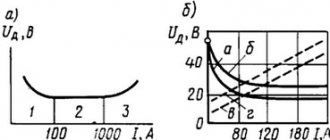
Current-voltage characteristic of a vacuum diode
This characteristic consists of the classic three steps:
- Nonlinear part. The volt-ampere characteristic of the diode at the point of current supply increases at a small rate. This is explained by the effect of counteracting the anode field by the negative voltage of free electrons. In this area, the anode current is extremely low. The effect of stress on force is exponential.
- The second part of the curve is described by the law of power 3/2. The effect of electricity on the anode from the applied voltage in this case is written by the three-second formula, in which the voltage at the anode is multiplied by a constant, the characteristics of the electrode dimensions.
- Saturation voltage. If the anode voltage continues to increase in proportion to previous values, the rate of increase in output current decreases. It is impossible to increase the output power due to the lack of free electrons.
Principle of operation
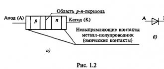
Semiconductor or rectifier diodes have a fairly simple operating principle. As we have already said, a diode is made of silicon in such a way that one end is p-type and the other end is n-type. This means that both pins have different characteristics. One has an excess of electrons, while the other has an excess of holes. Naturally, there is a region in the device in which all the electrons fill certain gaps. This means that there are no external charges. Due to the fact that this region is depleted of charge carriers and is known as the combining region.
Photo - principle of operation
Despite the fact that the connecting area is very small (often its size is several thousandths of a millimeter), current cannot flow in it in the usual way. If a voltage is applied such that the p-type area becomes positive and the n-type area becomes negative, the holes move to the negative pole and help electrons pass through the combining area. In the same way, electrons move to the positive contact and, as it were, bypass the unifying one. Despite the fact that all the particles move with different charges in different directions, they ultimately form a unidirectional current, which helps to rectify the signal and prevent voltage surges at the diode contacts.
If voltage is applied to a semiconductor diode in the opposite direction, no current will flow through it. The reason is that the holes are attracted by the negative potential, which is in the p-type region. Likewise, electrons are attracted to a positive potential that is applied to the n-type region. This causes the combining region to increase in size, making it impossible for directed particle flow to occur.
Photo - characteristics of semiconductors
How does a diode work?
Diode Polarity
A diode is a semiconductor device that has one-way conductivity. This characteristic appears due to the characteristics of the pn junction and the resistance at its ends. One-way conductivity means that the radio component will pass electric current only if there is a higher potential at the anode (input). If the power is higher at the cathode, reverse current appears. However, due to the high degree of resistance, the magnitude of such electric current is critically small. In this way, the current-voltage characteristic of the semiconductor device is constructed.
I-V characteristic of a real semiconductor diode
However, in practice, due to its semiconductor structure, a real diode has a number of disadvantages and limitations compared to an ideal diode. This can be seen in the graph below.
Vϒ(gamma) - conductivity threshold voltage
When switched on directly, the voltage across the diode must reach a certain threshold value - Vϒ. This is the voltage at which the PN junction in the semiconductor opens enough for the diode to begin conducting current well. Before the voltage between the anode and cathode reaches this value, the diode is a very poor conductor. Vϒ for silicon devices is approximately 0.7V, for germanium devices - about 0.3V.
ID_MAX - maximum current through the diode when connected directly
When connected directly, the semiconductor diode can withstand a limited current ID_MAX. When the current through the device exceeds this limit, the diode overheats. As a result, the crystal structure of the semiconductor is destroyed, and the device becomes unusable. The magnitude of this current varies greatly depending on the different types of diodes and their manufacturers.
IOP – reverse leakage current
When switched in reverse, the diode is not an absolute insulator and has a finite resistance, albeit a very high one. This causes leakage current or reverse current IOP to form. The leakage current for germanium devices reaches up to 200 µA, for silicon devices up to several tens of nA. The latest high quality silicon diodes with extremely low reverse current are around 0.5 nA.
PIV(Peak Inverse Voltage) - Breakdown voltage
When reverse-connected, the diode can withstand a limited voltage - the breakdown voltage PIV. If the external potential difference exceeds this value, the diode sharply lowers its resistance and turns into a conductor. This effect is undesirable, since the diode should only be a good conductor when connected directly. The breakdown voltage varies depending on the different types of diodes and their manufacturers.
Parasitic capacitance of PN junction
Even if a voltage significantly higher than Vϒ is applied to the diode, it will not immediately begin to conduct current. The reason for this is the parasitic capacitance of the PN junction, which takes some time to fill. This affects the frequency characteristics of the device.
Operating principle of a vacuum type diode
What is a diode - operating principle and device
When electricity is applied to the output of a vacuum diode, electrons leave the surface due to thermionic emission effect. Moreover, with the accumulation of free charged particles in the atmosphere, an area appears that is characterized by a negative potential. A characteristic feature of the vacuum device is that at this time the anode surfaces will begin to be positively charged. Because of this, subsequent charged particles will require a higher level of charge to break away. As a result of transient processes, a cloud of charged particles is formed around the cathode.
Interesting. A small part of the electrons is returned to the output of the radio component. At a temperature that corresponds to the required one and the cloud is stabilized, the output and return of charged particles from the cathode are equalized, which ensures stable movement of charged particles.
Diode classification:
By installation method:
- for surface mounting (SMD/SMT);
- for surface mounting (TH);
- integral (thin film).
By purpose:
- Rectifiers;
- Pulse;
They have a short duration of transient processes and are intended for use in pulsed operating modes.
- Detector;
- Mixing;
Designed to convert high-frequency signals into signals of a difference frequency determined by the frequency of the master oscillator.
- Switchable;
Used in microwave power level control devices.
- Restrictive;
- Protective;
Protection of equipment from increased mains voltage.
- Generating;
Used to generate HF and microwave oscillations.
- Reception;
- Radiative.
By design:
- Schottky diode;
- Microwave diode;
- Zener diode (Zener diode);
- Varicap;
- Light-emitting diode;
- Photodiode;
- Pin diode;
- Avalanche diode;
- Avalanche diode;
- Gunn diode;
- Tunnel diode;
- Reversed diode.
By p-n junction size:
- planar;
- point.
By frequency range:
- Low frequency;
- High frequency;
- Microwave.
Electric current in a vacuum
Current density - what is it and how is it measured?
To make it possible to transmit current in a vacuum, it is necessary to add free charged particles into space using emission phenomena:
- Thermionic - is the process of releasing charged particles by metals during heating. The speed of the process depends on the area, heating conditions and material properties. When kinetic energy exceeds the strength of electronic bonds, particles are released;
- Photoelectronic - occurs under the influence of lighting.
- Field emission occurs due to the influence of the electric field.
Device
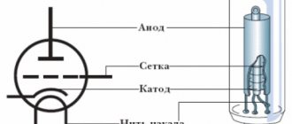
A semiconductor electrical diode or diode valve is a device that is made of semiconductor materials (usually silicon) and operates only with a one-way flow of charged particles. The main component is the crystal part, with a pn junction, which is connected to two electrical contacts. Vacuum diode tubes have two electrodes: a plate (anode) and a heated cathode.
Photo - semiconductor diode
Germanium and selenium are used to create semiconductor diodes, just as they were more than 100 years ago. Their structure allows the parts to be used to improve electronic circuits, convert alternating and direct current into unidirectional pulsating current, and to improve various devices. In the diagram it looks like this:
Photo - diode designation
There are different types of semiconductor diodes, their classification depends on the material, operating principle and area of use: zener diodes, pulsed, alloy, point, varicaps, laser and other types. Quite often analogues of bridges are used - these are planar and polycrystalline rectifiers. Their communication is also carried out using two contacts.
The main advantages of a semiconductor diode:
- Full interchangeability;
- Excellent throughput parameters;
- Availability. You can buy them at any electrical goods store or remove them for free from old circuits. The price starts from 50 rubles. Our stores offer both domestic brands (KD102, KD103, etc.) and foreign ones.
Diode Forward and Reverse Voltage
The level of power at which an appliance is open and electricity flows through it is called current. Reverse voltage is negative power that flows from the cathode to the anode. In the case of forward voltage, the level of obstruction to the movement of charged particles is not higher than 100 Ohms, but with reverse voltage the level of resistance increases several hundred times and can reach millions of Ohms.
Diode Forward and Reverse Voltage
Dependence of the diode barrier capacitance on voltage.
Let us present a graph of the dependence of the total capacitance CD of a 2D212A silicon diode on the reverse voltage (the main contribution to the total capacitance is made by the barrier capacitance) (Fig. 1.30).
For this diode, the maximum constant (average) forward current is 1 A, the maximum constant (pulse) reverse voltage is 200 V.
I-V characteristics and rectifier diode
The diode's current-voltage characteristic consists of several quadrants:
- In the first case, the device has high conductivity, which corresponds to the applied voltage;
- In the second part, the radio-electronic device receives current until it saturates, then resets;
- In the subsequent segment there is a reverse branch of the diode’s current-voltage characteristic. The approximation of this state indicates low conductivity.
I-V characteristics of the zener diode
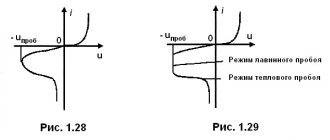
Electrical breakdown:
Electrical breakdown occurs due to a sharp increase in reverse current due to a sharp decrease in the resistance of the barrier layer.
An attentive reader will immediately object: “how can this be? After all, an increase in the reverse voltage for a pn junction causes an increase in the geometric dimensions of the blocking layer, and, consequently, its resistance!” And this matter is explained quite simply. Reality always comes up with some difficulties for us, so in semiconductors there are two phenomena - avalanche charge multiplication and the tunnel effect, by name, which divide electrical breakdown into avalanche and tunnel. And if to understand the first effect it is enough to read about its essence, then the tunnel effect is a quantum effect, and to understand it you simply need to strain your brain. Avalanche charge multiplication occurs due to the phenomenon of impact ionization, the essence of which is that electrons, accelerated by an electric field, acquire energy sufficient to knock electrons out of the atoms of the semiconductor crystal lattice, which in turn are also accelerated by this field, and the so-called “avalanche” process of electron separation from atoms by an electric field. The result of these processes is a sharp increase in conductivity, and, consequently, a decrease in the resistance of the barrier layer with virtually no change in its geometric dimensions.
The tunnel effect (also known as the Zener effect in English literature) is most likely in pn junctions of small thickness. Its essence is that electrons having a total energy less than the height of the energy barrier still penetrate through this energy barrier, in our case the barrier of the pn junction, without changing energy, at such voltages when the conduction band in the n-region has equal energy levels with a p-region valence band. This effect is completely quantum and contradicts classical mechanics. As a simplified explanation, we can say the following. From the solution of the Schrödinger equation for the problem of a potential barrier, it follows that the barrier transparency coefficient is non-zero for particles with an energy equal to or less than the height of this barrier. Well, in order to eliminate possible logical difficulties, we can recall the uncertainty relation (Heisenberg relation), which says that if we reduce the uncertainty in the coordinate of a particle, then we increase the uncertainty in the momentum, and vice versa. Consequently, We cannot say with certainty that the particle that passed the barrier actually had a certain energy at the moment of passage.
It should also be noted that the tunnel effect is probabilistic in nature, so the highest probability of its occurrence is in pn junctions with a high concentration of impurities.
What does the marking mean?
Typical markings:
- The first symbol is D – diode;
- The second is numbering, which corresponds to the type of element, material and method of application;
- The third is the type of device.
The volt-ampere characteristic of a diode shows the main parameters of the diode. Using the graph, you can obtain accurate information about the dependence of the voltage value at the diode output on the input voltage. There are several types of diodes: ideal and real, rectifier and zener diode, silicon and germanium, as well as LED and vacuum. The differences between them are in the work performed. In this case, the formula for the output voltage in the circuit will differ slightly. Since laboratory conditions are rare, minor errors may occur during startup and subsequent operation of the device. The current-voltage characteristic of a semiconductor assembly varies significantly from type to type, different characteristics can be significant.
Parasitic properties of the diode:
Temperature influence:
Since drift processes in a semiconductor play an important role, temperature can significantly change the current-voltage characteristics of the pn junction and, accordingly, the parameters of the diode.
Figure 3 - Effect of temperature on the diode's current-voltage characteristic.
Where:
— normal ambient temperature ();
— operating temperature of the diode.
Bottom line
Without pretending to be accurate, a device made from an Arduino Nano, 2 capacitors and 3 resistors allows you to compare the current-voltage characteristics of different two-terminal devices. Disadvantages include:
- Small voltage range. If you expand the range, the number of elements increases significantly.
- PWM noise. This can be eliminated by increasing the capacitor capacitance, increasing resistor values and installing additional filter stages, or by abandoning PWM in favor of a separate DAC or digital potentiometer.
- Small currents such as reverse currents of diodes are not visible. Also a removable drawback.
Photo of the hardware: