Current-voltage characteristic (volt-ampere characteristic) semiconductor Current-voltage characteristic (volt-ampere characteristic) semiconductor diode at direct current (static characteristic).
The current-voltage characteristic is the dependence of the current i flowing through the diode on the voltage u applied to the diode (Fig. 1.25). The graph of this dependence is also called the current-voltage characteristic.
First, we will assume (see Fig. 1.25) that the reverse voltage (u<0) is less than the breakdown voltage of the pn junction. Then, to a first approximation, we can assume that the current-voltage characteristic of the diode is determined by the already considered idealized description of the characteristics of the pn junction: i=is (eu/φr- 1)
The thermal current is due to the generation of minority carriers in areas adjacent to the pn junction region. However, this idealized description often produces unacceptable errors. A particularly large error occurs when calculating the diode current connected in the reverse direction (U < 0, i < 0). The current calculated from the expression under consideration (i= -is at |u| >> (φт)) for silicon diodes turns out to be several orders of magnitude less than the real one. At the same time, it is worth noting that in some calculations the reverse current can be neglected altogether.
Let us indicate the reasons for the difference between the characteristics of real diodes and idealized ones. Let us turn to the direct branch of the current-voltage characteristic of the diode (u> 0,i> 0). It differs from the idealized one due to the fact that in the real case it is influenced by:
- resistance of semiconductor layers (especially base);
- resistance of metal-semiconductor contacts.
It is important to note that the base resistance can significantly depend on the injection level (the injection level shows how the concentration of injected minority carriers in the base at the transition boundary relates to the concentration of majority carriers in the base). The influence of these resistances leads to the fact that the voltage on a real diode at a given current is slightly higher (usually by fractions of a volt) than it follows from the formula.
Let's turn to the reverse branch (u< 0, i < 0). The main reasons that the actual reverse current is usually several orders of magnitude greater than the current is are the following:
- thermal generation of carriers directly in the region of the pn junction;
- surface leaks.
Thermal generation in the region of the pn junction has a significant effect on the current because the transition region is depleted of mobile charge carriers, and the recombination process (reverse to the generation process and, in a certain sense, balancing it) is slowed down here.
At room temperature for silicon devices, the thermal generation current usually significantly exceeds the thermal current is.
For approximate calculations, we can assume that with increasing temperature, the current is doubles approximately every 5°C, and the thermal generation current doubles approximately every 10°C. At a temperature of about 100°C, the current is compared with the thermal generation current.
Surface leakage often accounts for the vast majority of reverse current. Their reasons are:
- surface energy levels providing active processes of generation and recombination;
- molecular and ionic films shunting the pn junction.
As the reverse voltage modulus increases, the leakage current first changes linearly and then more rapidly. The leakage current is characterized by the so-called “creep” - a change over time from several seconds to several hours.
In practical approximate calculations, it is sometimes assumed that the total reverse current of a silicon diode increases by 2 times or 2.5 times for every 10°C.
For example, let’s depict the characteristics of the rectifying silicon diode D229A at different temperatures (maximum average forward current - 400 mA, maximum pulse reverse voltage - 200 V). Direct branches of characteristics are presented in Fig. 1.26, and the reverse ones (before the breakdown mode) are shown in Fig. 1.27.
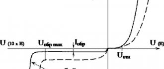
Let us turn to the breakdown mode of the semiconductor diode and the corresponding section of the reverse branch of the current-voltage characteristic (this section is not shown in Fig. 1.27).
Diodes of many specific nominal values are not designed to operate in breakdown mode. For them, this mode of operation is emergency. If during a breakdown the current in the circuit is not limited (for example, by external resistance), then the diode fails. In such devices, when the reverse voltage (modulo) increases excessively, thermal breakdown begins almost immediately (the electrical breakdown section is practically absent).
The breakdown onset voltage for the diodes under consideration is an unstable value (breakdown begins at u= -urob, where uprob is the so-called breakdown voltage and is a positive value). Let us depict the corresponding current-voltage characteristic (Fig. 1.28).
Some specific types of diodes are designed to operate in avalanche mode for a short period of time. Such diodes are called avalanche diodes. If the period of time during which the diode is in avalanche breakdown mode is short, then its pn junction does not have time to overheat and the diode does not fail.
Otherwise, the avalanche breakdown will turn into a thermal breakdown and the diode will fail.
Let us depict the current-voltage characteristic for an avalanche diode (Fig. 1.29).
Avalanche diodes, as a rule, are more reliable compared to conventional short-term diodes (overvoltages do not damage the avalanche diode).
For some specific types of diodes, breakdown mode is the main operating mode. These are the so-called zener diodes, discussed below.
What it is
VAC stands for current-voltage characteristic of a diode semiconductor. It reflects the dependence of the current that passes through the pn junction of the diode. The current-voltage characteristic determines the dependence of the current on the magnitude, as well as the polarity of the applied voltage. The current-voltage characteristic has the form of a graph (diagram). This graph looks like this:
I-V characteristic for a diode
For each type of diode, the current-voltage characteristic graph will have its own specific appearance. As you can see, the graph contains a curve. The values of forward current (direct connection) are marked vertically at the top, and in reverse at the bottom. But the horizontal diagram and graph display the voltage, similarly in the forward and reverse directions. Thus, the current-voltage characteristic diagram will consist of two parts:
- upper and right part - the element operates in the forward direction. It reflects the passing current. The line in this part goes sharply upward. It characterizes a significant increase in forward voltage;
- lower left part - the element acts in the opposite direction. It corresponds to the closed (reverse) current through the junction. Here the line runs almost parallel to the horizontal axis. It reflects the slow increase in reverse current.
Note! The steeper the vertical top part of the graph is, and the closer the bottom line is to the horizontal axis, the better the rectifying properties of the semiconductor will be.
It is worth noting that the current-voltage characteristic strongly depends on the ambient temperature. For example, an increase in air temperature can lead to a sharp increase in the reverse current. You can build a current-voltage curve with your own hands as follows:
- take the power supply;
- connect it to any diode (minus to the cathode, plus to the anode);
- We take measurements using a multimeter.
From the data obtained, the current-voltage characteristic for a specific element is constructed. Its diagram or graph may look like this.
Nonlinear current-voltage characteristic
The graph shows the current-voltage characteristic, which in this design is called nonlinear. Let's look at examples of different types of semiconductors. For each individual case, this characteristic will have its own schedule, although they will all be of the same nature with only minor changes.
Marking
In order to determine the type and find out the characteristics of a semiconductor diode, manufacturers apply special designations to the element body. It consists of four parts.
In the first place is a letter or number indicating the material from which the diode is made. Can take the following values:
- G (1) - germanium;
- K (2) - silicon;
- A (3) - gallium arsenide;
- And (4) - indium.
On the second - diode types. They can also have different meanings:
- D - rectifier;
- B - varicap;
- A - ultra-high frequency;
- I - tunnel;
- C - zener diodes;
- C - rectifying posts and blocks.
In third place is a number indicating the area of application of the element.
The fourth place is numbers from 01 to 99, indicating the serial number of the development.
Additional markings may also be applied to the body. But, as a rule, they are used in specialized devices and circuits.
For ease of perception, diodes can also be marked with various graphic symbols, for example, dots and stripes. There is no particular logic in such drawings. That is, to determine what kind of diode it is, you will have to look at a special correspondence table.
CVC for shotky
One of the most common diodes today is Schottky. This semiconductor was named after the German physicist Walter Schottky. For Schottky, the current-voltage characteristic will have the following form.
CVC for Schottky
As you can see, Schottky is characterized by a low voltage drop in a direct connection situation. The graph itself is clearly asymmetrical. In the forward displacement zone, an exponential increase in current and voltage is observed. Under reverse and forward bias for a given element, the current in the barrier is due to electrons. As a result, such elements are characterized by rapid action, since there are no diffuse and recombination processes. In this case, the asymmetry of the current-voltage characteristic will be typical for barrier-type structures. Here, the dependence of current on voltage is determined by a change in the number of carriers that take part in charge transfer processes.
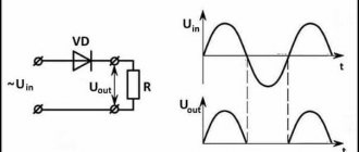
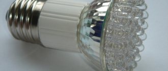
LED connection.
The simplest way to connect an LED is to connect it with a resistor. The latter is necessary for current limiting to prevent LED burnout during voltage surges.
When connecting LED elements according to any scheme, do not forget to maintain polarity! Otherwise, the semiconductor device will not glow and will burn out.
Electrical diagram for connecting an LED (LED) and a resistor (R).
When connecting several light-emitting diodes, different options for connecting them are possible.
Serial connection.
Serial connection diagram.
The elements are connected in series, taking into account polarity. In the circuit, the current value is constant, and the voltage across the LED elements is summed up.
Parallel connection.
Diagram of parallel connection of LEDs through one resistor.
In this case, the voltage in the circuit remains constant, and the currents on the elements add up. This type of connection has a disadvantage. Different LEDs may have different voltage drops. Therefore, the current on any element may exceed the permissible value, which will lead to breakdown.
To avoid this, you should connect a different resistor to each parallel circuit.
Parallel connection diagram.
Parallel-serial connection.
When connecting a large number of LEDs, it is worth using a parallel-series electrical circuit. At the same time, the voltage in parallel branches is the same.
Electrical diagram of parallel-series connection.
Silicon diode and its current-voltage characteristic
In addition to Schottky, silicon semiconductors are very popular at the moment. For a silicon type diode, the current-voltage characteristic looks like this.
I-V characteristics of silicon and germanium diode
For such semiconductors, this characteristic begins at approximately 0.5-0.7 Volts. Very often, silicon semiconductors are compared with germanium semiconductors. If the ambient temperatures are equal, then both devices will exhibit bandgap. In this case, a silicon element will have a lower forward current than one made from germanium. The same rule applies to reverse current. Therefore, germanium semiconductors usually immediately experience thermal breakdown if there is a high reverse voltage. As a result, in the presence of the same temperature and forward voltage, the potential barrier for silicon semiconductors will be higher and the injection current lower.
I-V characteristics and rectifier diode
In conclusion, I would like to consider this characteristic for a rectifier diode. A rectifier diode is one of the types of semiconductor that is used to convert alternating current to direct current.
I-V characteristic for a rectifier diode
The diagram shows the experimental current-voltage characteristic and the theoretical one (dashed line). As you can see, they do not match. The reason for this lies in the fact that some factors were not taken into account for theoretical calculations:
- the presence of ohmic resistance in the base and emitter regions of the crystal;
- his findings and contacts;
- the possibility of leakage currents along the crystal surface;
- the occurrence of recombination and generation processes in the transition for carriers;
- various types of breakdowns, etc.
All these factors can have different effects, leading to a real current-voltage characteristic that differs from the theoretical one. Moreover, the ambient temperature has a significant impact on the appearance of the graph in this situation. The current-voltage characteristic for a rectifier diode demonstrates the high conductivity of the device when a voltage is applied to it in the forward direction. In the opposite direction, low conductivity is observed. In such a situation, current practically does not flow through the element in the opposite direction. But this only happens at certain reverse voltage parameters. If it is exceeded, then the graph shows an avalanche-like increase in the current in the opposite direction.
General information
Diode (D) is a semiconductor element that serves to pass current through a pn junction in only one direction. With the help of D, you can straighten the variable U, obtaining a constant pulsating one from it. To smooth out ripples, capacitor or inductive filters are used, and sometimes they are combined.
D consists only of a pn junction with leads called anode (+) and cathode (-). Current, when passing through a conductor, has a thermal effect on it. When heated, the cathode emits negatively charged particles - electrons (E). The anode attracts electrons because it has a positive charge. In the process, an emission field is formed, in which a current (emission) occurs. Between (+) and (-) a negative spatial charge is generated, which interferes with the free movement of electrons. Electrons that reach the anode form an anodic current, and those that do not reach the cathode. If the anode and cathode currents are zero, D is in the closed state.
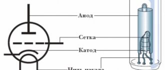
Semiconductor device
D consists of a housing made of durable dielectric material. The housing contains a vacuum space with 2 electrodes (anode and cathode). Electrodes representing a metal with an active layer are indirectly heated. The active layer emits electrons when heated. The cathode is designed in such a way that there is a wire inside it that glows and emits electrons, and the anode serves to receive them.
In some sources, the anode and cathode are called a crystal, which is made of silicon (Si) or germanium (Ge). One of its components has an artificial deficiency of electrons, and the other has an excess (Fig. 1). There is a boundary between these crystals, which is called a pn junction.
Figure 1 - Schematic representation of a pn-type semiconductor.
Areas of application
D is widely used as an AC rectifier in the construction of power supplies (PSUs), diode bridges, and also as a single element of a specific circuit. D is able to protect the circuit from non-compliance with the polarity of the power source connection. A breakdown of any semiconductor part (for example, a transistor) may occur in the circuit and lead to the process of failure of the chain of radio elements. In this case, a chain of several D connected in the opposite direction is used. Switches are created based on semiconductors for switching high-frequency signals.
D are used in the coal and metallurgical industries, especially when creating intrinsically safe switching circuits in the form of diode barriers that limit U in the required electrical circuit. Diode barriers are used together with current limiters (resistors) to reduce I values and increase the degree of protection, and therefore the electrical safety and fire safety of the enterprise.