We continue to disassemble everything related to transistors and today we have one of the most commonly used connection circuits. Namely, the circuit for connecting a bipolar transistor with a common emitter (CE) . In addition, based on this circuit, we will consider the main parameters and characteristics of a bipolar transistor. The topic is important, so without further ado, let's get down to business.
The name of this scheme largely explains its basic idea. Since the circuit is with a common emitter, then, in fact, the emitter is a common electrode for the input and output circuits. This is what the OE circuit looks like for an npn transistor:
And like this for pnp:
Let's look at all the processes again for the case using an NPN transistor. For pnp, the essence remains the same, only the polarity changes.
The input quantities are the base-emitter voltage (U_{be}) and the base current (I_{b}), and the output quantities are the collector-emitter voltage (U_{ke}) and the collector current (I_{k}). Please note that in these circuits we do not have a load in the collector circuit, therefore all the characteristics that we will consider further are called static. In other words, the static characteristics of a transistor are the relationships between voltages and currents at the input and output when there is no load.
Device and principle of operation
Depending on the principle of operation and design features, transistors are divided into two large classes: bipolar and field-effect.
A bipolar transistor is a semiconductor device with two interacting pn junctions and three or more terminals.
The semiconductor crystal of a transistor consists of three regions with alternating types of electrical conductivity, between which there are two pn junctions. The middle region is usually very thin (fractions of a micron), so the pn junctions are located close to each other.
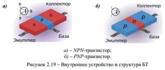
Depending on the order of alternation of semiconductor regions with different types of electrical conductivity, transistors of p-p-p and p-p-n types are distinguished. Simplified structures and UGOs of different types of transistors are shown in Figure 1.23, a, b.
a b
Figure 1.23 – Structure and UGO of bipolar transistors
The bipolar transistor is the most common active semiconductor device. Silicon is currently used as the main material for the manufacture of bipolar transistors. In this case, p-p-n-type transistors are predominantly manufactured, in which the main charge carriers are electrons, which have a mobility two to three times higher than the mobility of holes.
The amount of current flowing in the output circuit (in the collector or emitter circuit) of the bipolar transistor is controlled using the current in the circuit of the control electrode - base. The base is the middle layer in the transistor structure. The outermost layers are called emitter (to emit, spew out) and collector (to collect). The concentration of impurities (and, consequently, the main charge carriers) in the emitter is significantly greater than in the base and greater than in the collector. Therefore, the emitter region has the lowest resistance .
To illustrate the physical processes in a transistor, we will use the simplified structure of a n-p-n-type transistor shown in Figure 1.24. To understand the operating principle of a transistor, it is extremely important to take into account that the pn junctions of the transistor strongly interact with each other. This means that the current of one junction greatly affects the current of the other, and vice versa.
In the active mode (when the transistor operates as an amplifier element), two power sources are connected to the transistor so that the emitter junction is forward biased and the collector junction is reverse biased (Figure 1.24). Under the influence of the electric field of the EBE source, a fairly large forward current IE flows through the emitter junction, which is provided mainly by the injection of electrons from the emitter into the base. The injection of holes from the base into the emitter will be insignificant due to the above-mentioned difference in the concentrations of impurity atoms.
Figure 1.24 – Physical processes in a bipolar transistor
The flow of electrons providing current IE through the emitter-base junction is shown in Figure 1.24 with a wide arrow. Part of the electrons injected into the base region (1 ... 5%) recombine with the main charge carriers for this region - holes, forming a current IB in the external circuit of the base. Due to the large difference in the concentrations of the main charge carriers in the emitter and base, uncompensated electrons injected into the base move deep into it towards the collector.
Near the collector pn junction, electrons are exposed to the accelerating electric field of this reverse biased junction. And since they are minority carriers in the base, electrons are drawn ( extracted ) into the collector region. In the collector, electrons become the main charge carriers and easily reach the collector terminal, creating a current in the external circuit of the transistor.
Thus, the current through the base terminal of the transistor is determined by two counter-directed current components. If there were no recombination processes in the base, then these currents would be equal to each other, and the resulting base current would be equal to zero. But since recombination processes exist in any real transistor, the current of the emitter pn junction is slightly greater than the current of the collector pn junction.
For the collector current we can write the following equality
, (1.9)
where ast is the static transfer coefficient of the emitter current;
IKBO is the reverse current of the collector junction (thermal current) (for low-power transistors at normal temperature it is 0.015 ... 1 μA).
In practice, the static transfer coefficient of the emitter current ast, depending on the type of transistor, can take values in the range of 0.95 ... 0.998.
The emitter current in the transistor is numerically the largest and is equal to
, (1.10)
where
, (1.11)
where is the static transfer coefficient of the base current in a circuit with a common emitter (in the reference literature the designation h21E is used, usually takes the value bst = 20 ... 1000 depending on the type and power of the transistor).
From what was said earlier, it follows that the transistor is a controlled element, since the value of its collector (output) current depends on the values of the emitter and base currents.
Concluding our consideration of the operating principle of a bipolar transistor, it should be noted that the resistance of the reverse-biased collector junction (when reverse voltage is applied to it) is very high (hundreds of kilo-ohms). Therefore, load resistors with very high resistances can be included in the collector circuit, thereby practically without changing the value of the collector current. Accordingly, significant power will be released in the load circuit.
The resistance of a forward-biased emitter junction, on the contrary, is very small (tens - hundreds of Ohms). Therefore, at almost identical values of the emitter and collector currents, the power consumed in the emitter circuit turns out to be significantly less than the power allocated in the load circuit. This indicates that the transistor is a power amplifying semiconductor device.
The manufacturing technology of bipolar transistors can be different: fusion, diffusion, epitaxy. This largely determines the characteristics of the device. Typical structures of bipolar transistors manufactured by various methods are shown in Figure 1.25. In particular, Figure 1.25, a shows the structure of alloy, Figure 1.25, b - epitaxial-diffusion, Figure 1.25, c - planar, Figure 1.25, d - mesaplanar transistors.
Figure 1.25 – Methods for manufacturing bipolar transistors
Step-by-step instructions for checking with a multimeter
Before starting the test, first of all, the structure of the triode device is determined, which is indicated by the emitter junction arrow. When the direction of the arrow points towards the base, then this is the PNP variant, the direction opposite to the base indicates NPN conductivity.
Testing a PNP transistor with a multimeter consists of the following sequential operations:
- We check the reverse resistance; to do this, we connect the “positive” probe of the device to its base.
- The emitter junction is tested; for this we connect the “negative” probe to the emitter.
- To check the collector, move the negative probe onto it.
The results of these measurements should show a resistance within the value of “1”.
To check direct resistance, swap the probes:
- We attach the “negative” probe of the device to the base.
- We alternately move the “positive” probe from the emitter to the collector.
- On the multimeter screen, the resistance readings should be from 500 to 1200 Ohms.
These readings indicate that the transitions are not broken, the transistor is technically sound.
Many amateurs have difficulty identifying the base, and, accordingly, the collector or emitter. Some advise starting to determine the base, regardless of the type of structure, in this way: alternately connecting the black probe of the multimeter to the first electrode, and the red probe alternately to the second and third.
The base will be detected when the voltage across the device begins to drop. This means that one of the transistor pairs has been found - “base-emitter” or “base-collector”. Next, you need to determine the location of the second pair in the same way. The common electrode of these pairs will be the base.
It will be interesting➡ How to take measurements with a megohmmeter
Verification methods
Any repair of electronics and electrical equipment begins with an external inspection, and then proceeds to measurements. This approach allows you to localize most faults. To find a varistor on the board, look at the figure below - this is what varistors look like. Sometimes they can be confused with capacitors, but can be distinguished by their markings.
If the element is burnt out and the markings cannot be read, look at this information on the device diagram. On the board and in the diagram it can be designated by the letters RU. The conventional graphic symbol looks like this.
There are three ways to test a varistor quickly and easily:
- Visual inspection.
- Call. This can be done with a multimeter or any other device that has a continuity test function.
- Resistance measurement. This can be done with a high-range ohmmeter, multimeter or megger.
A varistor fails when a large or prolonged current passes through it. Then the energy is dissipated in the form of heat, and if its amount is greater than that determined by the design, the element burns out. The housing of these components is made of a hard dielectric material, such as ceramic or epoxy coating. Therefore, when it fails, the integrity of the outer coating is most often damaged.
You can visually check the varistor for functionality - there should be no cracks on it, as in the photo:
The next method is to check the varistor with a tester in continuity mode. This cannot be done in the circuit, because the dialing can work through parallel-connected elements. Therefore, you need to unsolder at least one of its legs from the board.
Important: you should not check the elements for serviceability without desoldering them from the board - this may give false readings from the measuring instruments. Since in the normal state (without voltage applied to the terminals) the resistance of the varistor is high, it should not ring through. The test is performed in both directions, that is, by swapping the multimeter probes twice
The test is performed in both directions, that is, by swapping the multimeter probes twice
Since in the normal state (without voltage applied to the terminals) the resistance of the varistor is high, it should not ring through. The test is performed in both directions, that is, by swapping the multimeter probes twice.
On most multimeters, the continuity mode is combined with the diode testing mode. It can be found by the diode icon on the mode selector scale. If there is a sound indication sign next to it, it probably also has a dial tone.
Another way to test a varistor for breakdown with a multimeter is to measure the resistance. You need to set the device to the maximum measurement limit, in most devices this is 2 MOhms (megaohms, designated as 2M or 2000K). The resistance must be equal to infinity. In practice, it can be lower, within 1-2 MOhm.
Interesting! The same can be done with a megaohmmeter, but not everyone has one. It is worth noting that the voltage at the megohmmeter terminals should not exceed the classification voltage of the component being tested.
This ends the available methods for checking a varistor. This time, the multimeter will help the radio amateur find the faulty element, as in a large number of other cases. Although in practice a multimeter is not always needed in this matter, because the matter rarely goes beyond a visual inspection. Replace the burnt element with a new one, designed for voltage and with a diameter no less than the burnt one, otherwise it will burn out even faster than the previous one.
Operating modes and transistor switching circuits
Each pn junction of the transistor can be supplied with both forward and reverse voltage. In accordance with this, there are four modes of operation of a bipolar transistor: cutoff mode, saturation mode, active mode and inverse mode.
The active mode is ensured by applying forward voltage to the emitter junction, and reverse voltage to the collector junction (the main operating mode of the transistor). This mode corresponds to the maximum value of the emitter current transfer coefficient and ensures minimal distortion of the amplified signal.
In the inverse mode, a forward voltage is applied to the collector junction, and a reverse voltage is applied to the emitter junction (ast ® min; used very rarely).
In saturation , both junctions are forward biased. In this case, the output current does not depend on the input current and is determined only by the load parameters.
In cutoff , both junctions are reverse biased. The output current is close to zero.
Saturation and cutoff modes are used simultaneously in key circuits (when the transistor is operating in switch mode).
When using a transistor in electronic devices, two terminals are needed to supply an input signal and two terminals to connect a load (receive an output signal). Since the transistor has only three terminals, one of them must be common for the input and output signals.
Depending on which terminal of the transistor is common when connecting the signal source and load, there are three transistor switching circuits: with a common base (CB) (Figure 1.26, a); with a common emitter (CE) (Figure 1.26, b); with a common collector (OC) (Figure 1.26, c).
In these circuits, constant voltage sources and resistors provide direct current operating modes for transistors, that is, the required voltages and initial currents. AC input signals are generated by I/O sources. They change the emitter (base) current of the transistor, and, accordingly, the collector current. Increments in the collector current (Figure 1.26, a, b) and emitter current (Figure 1.26, c) will create, respectively, voltage increments on the resistors RK and RE, which are the output signals.
a B C
Figure 1.26 – Transistor connection circuits
When determining the transistor switching circuit, it is necessary to take into account that the resistance of the constant voltage source for alternating current is close to zero.
What is a transistor?
In its modern meaning, a transistor is a semiconductor radio element designed to change the parameters of an electric current and control it. A conventional semiconductor triode has three terminals: a base, which receives control signals, an emitter, and a collector. There are also high power composite transistors.
The size scale of semiconductor devices is striking - from several nanometers (unpackaged elements used in microcircuits) to centimeters in diameter for high-power transistors intended for power plants and industrial equipment. Reverse voltages of industrial triodes can reach up to 1000 V.
Basic operating principle
At rest, no current flows between the collector and emitter of a bipolar triode. Electric current is prevented by the resistance of the emitter junction, which arises as a result of the interaction of the layers. To turn on the transistor, you need to apply a small voltage to its base.
The figure shows a diagram explaining the working principle of a triode.
Principle of operation
By controlling the base currents, you can turn the device on and off. If an analog signal is applied to the base, it will change the amplitude of the output currents. In this case, the output signal will exactly repeat the oscillation frequency at the base electrode. In other words, the electrical signal received at the input will be amplified.
Thus, semiconductor triodes can operate in electronic switch mode or in input signal amplification mode.
The operation of the device in electronic key mode can be understood from Figure 3.
Triode in switch mode
Designation on diagrams
The generally accepted designation is “VT” or “Q”, followed by a positional index. For example, VT 3. On earlier diagrams you can find outdated designations: “T”, “PP” or “PT”. The transistor is depicted as symbolic lines indicating the corresponding electrodes, circled or not. The direction of current in the emitter is indicated by an arrow.
Figure 4 shows a ULF circuit in which transistors are designated in a new way, and Figure 5 shows schematic images of different types of field-effect transistors.
Current-voltage characteristics of the transistor
The properties of a bipolar transistor are most fully described using static current-voltage characteristics. In this case, the input and output current-voltage characteristics of the transistor are distinguished. Since all three currents (base, collector and emitter) in the transistor are closely interconnected, when analyzing the operation of the transistor it is necessary to use simultaneously the input and output current-voltage characteristics.
Each transistor switching circuit has its own current-voltage characteristics, which represent a functional dependence of the currents through the transistor on the applied voltages. Due to the nonlinear nature of these dependencies, they are usually presented in graphical form.
A transistor, like a four-terminal network, is characterized by input and output static current-voltage characteristics, showing respectively the dependence of the input current on the input voltage (at a constant value of the output voltage of the transistor) and the output current on the output voltage (at a constant input current of the transistor).
Figure 1.27 shows the static current-voltage characteristics of a pnp transistor connected in a circuit with an OE (most often used in practice).
a b
Figure 1.27 – Static current-voltage characteristics of a bipolar transistor connected according to a circuit with an OE
The input current-voltage characteristic (Figure 1.27, a) is similar to the direct branch of the diode's current-voltage characteristic. It represents the dependence of the current IB on the voltage UBE at a fixed value of the voltage UKE, that is, a dependence of the form
. (1.12)
From Figure 1.27, a it is clear: the higher the voltage UKE, the more to the right the branch of the input current-voltage characteristic shifts. This is explained by the fact that with an increase in the reverse bias voltage UCE, the height of the potential barrier of the collector pn junction increases. And since the collector and emitter pn junctions in the transistor interact strongly, this, in turn, leads to a decrease in the base current at a constant voltage UBE.
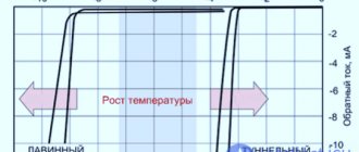
Static current-voltage characteristics, presented in Figure 1.27, a, were taken at normal temperature (20 °C). As the temperature increases, these characteristics will shift to the left, and as the temperature decreases, to the right. This is due to the fact that as the temperature rises, the intrinsic electrical conductivity of semiconductors increases.
For the output circuit of a transistor connected according to a circuit with an OE, a family of output current-voltage characteristics is constructed (Figure 1.27, b). This is due to the fact that the collector current of the transistor depends not only (and not so much, as can be seen from the figure) on the voltage applied to the collector junction, but also on the base current. Thus, the output current-voltage characteristic for a circuit with an OE is called the dependence of the current IK on the voltage UKE at a fixed current IB, that is, a dependence of the form
. (1.13)
Each of the output current-voltage characteristics of a bipolar transistor is characterized at the beginning by a sharp increase in the output current IK with an increase in the output voltage UKE, and then, as the voltage further increases, by a slight change in the current.
On the output current-voltage characteristic of the transistor, three regions can be distinguished, corresponding to different modes of operation of the transistor: the saturation region, the cutoff region and the region of active operation (amplification) , corresponding to the active state of the transistor when ½UBE ½ > 0 and ½UCE½> 0.
The input and output static current-voltage characteristics of transistors are used in graphic-analytical calculations of cascades containing transistors.
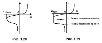
The static input and output current-voltage characteristics of a pnp-type bipolar transistor for a switching circuit with OB are shown in Figure 1.28, a and 1.28, b, respectively.
a b
Figure 1.28 – Static current-voltage characteristics of a bipolar transistor for a switching circuit with OB
For a circuit with an OB input static current-voltage characteristic, the dependence of the current IE on the voltage UEB at a fixed voltage value UKB is called, that is, the dependence is of the form
. (1.14)
The output static current-voltage characteristic for a circuit with OB is called the dependence of the current IK on the voltage UKB at a fixed current IE, that is, a dependence of the form
. (1.15)
In Figure 1.28, b, two areas can be distinguished, corresponding to two operating modes of the transistor: active mode (UKB < 0 and the collector junction is biased in the opposite direction); saturation mode (UCB > 0 and the collector junction is forward biased).
Why do you need a transistor?
I often have a question: why do we need a transistor? Why not connect the LED and resistor directly to the battery?
The advantage of a transistor is that you can use a small current or voltage to control a much larger current and voltage.
This is very useful if you want to control things like motors, high power LEDs, speakers, relays and more using a microcontroller/Raspberry Pi/Arduino. The output of the microcontroller can only provide a few milliamps at 5V. So if you want to control, for example, a 230V street light, you cannot do it directly with the microcontroller
You can use a relay instead. But even a relay usually requires more current than the microcontroller output can provide. Therefore you will need a transistor to drive the relay:
It will be interesting➡ Total current law for a magnetic field
Mathematical model of a bipolar transistor
To date, many electrical models of bipolar transistors are known. In computer-aided design (CAD) systems for radio-electronic equipment, the following are most often used: Ebers-Moll models, the generalized Hummel-Poon charge control model, the Linville model, as well as local P- and T-shaped models of Giacolleto linear increments.
Let us consider, as an example, one of the variants of the Ebers-Moll model (Figure 1.29), which reflects the properties of the transistor structure in linear operating mode and in cutoff mode.
Figure 1.29 – Equivalent circuit of a bipolar transistor (Ebers-Moll model)
In Figure 1.29 the following designations are used: rе, rb, rк – resistances, respectively, of the emitter, base and collector regions of the transistor and contacts to them; Ib, Ik – voltage-controlled current sources at the input junction, reflecting the transfer of current through the transistor; Reb – leakage resistance of the base-emitter junction; Rkb is the leakage resistance of the base-collector junction. The source current Ib is related to the voltage at the junction by the relation
, (1.15)
where IBO is the saturation current of the base-emitter junction (reverse current);
yк = (0.3 ... 1.2) V – contact potential difference (depending on the type of semiconductor material);
t – empirical coefficient.
Parallel to the base-emitter junction, the barrier capacitance Cbe and the diffusion capacitance Cde of the junction are included. The value of Cbe is determined by the reverse voltage at the junction and depends on it according to the law
, (1.16)
where C0b is the junction capacitance at ip = 0;
g = 0.3 ... 0.5 – coefficient depending on the distribution of impurities in the base area of the transistor.
The diffusion capacitance is a function of the current Ib flowing through the junction and is determined by the expression
, (1.17)
where A is a coefficient depending on the properties of the transition and its temperature.
The collector-base junction is modeled similarly, the only difference is that only the barrier capacitance of the junction is taken into account
, (1.18)
since when the transistor operates in linear mode and collector current cutoff mode, this transition is closed. The expression for the current of a controlled source of collector current, modeling the amplifying properties of the transistor, has the form
, (1.19)
where bst is the static transfer coefficient of the base current of the transistor in a circuit with a common emitter.
The parameters of the Ebers-Moll model can be obtained either by calculation based on the analysis of the physico-topological model of the transistor, or measured experimentally. The static parameters of the model are most easily determined using direct current.
The global electrical model of a discrete bipolar transistor, taking into account the inductance and capacitance of its terminals, is presented in Figure 1.30.
Figure 1.30 – Global model of a bipolar transistor
Applications of PNP transistors:
- PNP transistors are used as switches i.e. analog switches, emergency buttons, etc. They are used when emergency shutdown is required.
- These types of transistors are used in current source circuits, i.e., by taking advantage of the characteristics of the current flowing from the collector.
- Used in amplification circuits.
- They are used in paired Darlington circuits.
- PNP transistors are used in heavy-duty motors for current control and in various robot and microcontroller development applications.
Next
MiscellaneousWhat is active power?
Transistor pairs in electric motor control circuits
They are also used in H-bridge control circuits for reversible DC motors, which make it possible to regulate the current through the motor evenly in both directions of its rotation.
The H-bridge circuit above is so called because the basic configuration of its four transistor switches resembles the letter "H" with the motor located on the cross line. The transistor H-bridge is probably one of the most commonly used types of reversible DC motor control circuit. It uses “complementary” pairs of NPN and PNP transistors in each branch to act as switches to control the motor.
Control input A allows the motor to run in one direction, while input B is used for reverse rotation.
For example, when transistor TR1 is on and TR2 is off, input A is connected to the supply voltage (+Vcc), and if transistor TR3 is off and TR4 is on, then input B is connected to 0 volts (GND). Therefore, the motor will rotate in one direction, corresponding to the positive potential of input A and the negative potential of input B.
If the switch states are changed so that TR1 is off, TR2 is on, TR3 is on, and TR4 is off, the motor current will flow in the opposite direction, causing it to reverse.
By using opposite logic levels "1" or "0" on inputs A and B, you can control the direction of rotation of the motor.
Calculation of a switch for a transistor
Let's add a payload in the form of an LED to the circuit. Resistor R_k remains in place, it will limit the current through the load and ensure the required operating mode:
Suppose that to turn on the LED you need to apply a voltage of 3V (U_d) to it. In this case, the diode will consume a current equal to 50 mA (I_d). Let's set the transistor parameters (in real circuits, these values are taken from the documentation for the transistor used):
- Current gain h_{21e} = 100…500 (the range is always specified, not a specific value)
- The voltage drop across the base-emitter junction required to open this junction: U_{be} = 0.6 medspace V.
- Saturation voltage: U_{ke medspace us} = 0.1 medspace V.
We take specific values for calculations, but in practice everything is somewhat different. As you remember, the parameters of transistors depend on many factors, in particular on the operating mode, as well as on temperature. And the ambient temperature, of course, can change. It is not so easy to determine clear values from the characteristics, so you need to try to ensure a small margin. For example, when calculating, it is better to take the current gain equal to the minimum of the values given in the datasheet. After all, if the coefficient in reality is higher, then this will not disrupt the operation of the circuit; of course, the efficiency will be lower, but nevertheless the circuit will work. And if we take the maximum value of h_{21e}, then under certain conditions it may turn out that the real value turned out to be less, and it is no longer sufficient to ensure the required operating mode of the transistor.
So, let's return to the example. The input data for the calculation, among other things, are the voltages of the sources. In this case:
- E_{in} = 3.3medspace Q. I chose a typical value that is found in practice when developing circuits on microcontrollers. In this example, this voltage is turned on and off by switch S_1.
- E_{out} = 9medspace B.
First of all, we need to calculate the resistance of the resistor in the collector circuit. The voltages and currents of the output circuit in the on state are related as follows:
U_{ke medspace us} + U_{R_k} + U_d = E_{out}
In this case, according to Ohm's law:
U_{R_к} = I_к R_к
And we have a given current, since we know how much current the load (in this case, a diode) consumes when it is on. Then:
U_{R_k} = I_d R_kU_{ke medspace us} + I_d R_k + U_d = E_{out}
So, in this formula we know everything except the resistance, which needs to be determined:
R_к = frac{E_{out} medspace — medspace U_д medspace — medspace U_{ке medspace us}}{I_д} enspace= frac{9 medspace B medspace — medspace 3 medspace B medspace — medspace 0.1 medspace B}{0.05 medspace A} medspaceapprox 118 medspace Ohm.
It will be interesting➡ AC voltage. Does the outlet have direct current or alternating current?
We select an available resistance value from the standard range of ratings and get R_{к} = 120medspace Ohm. Moreover, it is important to choose a larger value. This is due to the fact that if we take a value slightly larger than calculated, then the current through the load will be slightly less. This will not lead to any malfunctions. If you take a smaller resistance value, this will lead to the fact that the current and voltage at the load will exceed the specified ones, which is worse
Let's recalculate the collector current value for the selected resistance value:
I_к = frac{U_{R_к}}{R_к} medspace = frac{9 medspace V medspace — medspace 3 medspace V medspace — medspace 0.1 medspace V}{120 medspace Ohm} medspaceapproxmedspace 49.17 medspace mA
It's time to determine the base current; for this we use the minimum gain value:
I_b = frac{I_к}{h_{21е}} = frac{49.17 medspace mA}{100} = 491.7 medspace μA
And the voltage drop across resistor R_b:
U_{R_b} = E_{in} medspace — medspace 0.6 medspace B = 3.3 medspace B medspace — medspace 0.6 medspace B = 2.7 medspace B
Now we can easily determine the resistance value:
R_b = frac{U_{R_b}}{I_b}medspace = frac{2.7 medspace V}{491.7 medspace μA} approx 5.49 medspace KOhm
Again we turn to a number of acceptable denominations. But now we need to choose a value less than the calculated one. If the resistor resistance is greater than the calculated value, then the base current will, on the contrary, be less. And this can lead to the fact that the transistor does not open completely, and when it is on, most of the voltage will drop across the transistor (U_{ke}), which, of course, is undesirable.
Therefore, we select a value of 5.1 KOhm for the base resistor. And this stage of calculation was the last! Let's recap, our calculated denominations were:
- R_{b} = 5.1medspace KOhm
- R_{k} = 120medspace Ohm
By the way, in a transistor switch circuit, a resistor is usually added between the base and emitter, with a nominal value of, for example, 10 KOhm. It is needed to tighten the base when there is no signal at the input. In our example, when S1 is open, the input simply hangs in the air. And under the influence of interference, the transistor will randomly open and close. Therefore, a pull-up resistor is added so that in the absence of an input signal, the base potential is equal to the emitter potential. In this case, the transistor will be guaranteed to be closed.
Today we went through the classical scheme, which I try to adhere to, that is, from theory to practice. I hope that the material will be useful, and if you have any questions, write in the comments, I will be happy to help!
Saturation mode
The mode differs from the active one in that the transistor opens completely and the collector current reaches the maximum possible value. Its increase can only be achieved by changing the applied EMF or load in the output circuit. When the base current changes, the collector current does not change. Saturation mode is characterized by the fact that the transistor is extremely open, and here it serves as a switch in the on state. Circuits for switching on bipolar transistors when combining cutoff and saturation modes make it possible to create electronic switches with their help.
All operating modes depend on the nature of the output characteristics shown in the graph.
They can be clearly demonstrated if a circuit for switching on a bipolar transistor with an OE is assembled.
If you plot on the ordinate and abscissa axes the segments corresponding to the maximum possible collector current and the value of the supply voltage VCC, and then connect their ends together, you will get a load line (red). It is described by the expression: IC = (VCC - VCE)/RC. It follows from the figure that the operating point, which determines the collector current IC and voltage VCE, will shift along the load line from bottom to top as the base current IB increases.
The area between the VCE axis and the first output characteristic (shaded), where IB = 0, characterizes the cutoff mode. In this case, the reverse current IC is negligible, and the transistor is turned off.
The uppermost characteristic at point A intersects with the direct load, after which, with a further increase in IB, the collector current no longer changes. The saturation zone in the graph is the shaded area between the IC axis and the steepest characteristic.
Operation of a PNP transistor stage
So, to cause base current to flow in a PNP transistor, the base must be more negative than the emitter (current must leave the base) by about 0.7 volts for a silicon device or 0.3 volts for a germanium device. The formulas used to calculate base resistor, base current or collector current are the same as those used for an equivalent NPN transistor and are presented below.
We see that the fundamental difference between an NPN and a PNP transistor is the correct biasing of the pn junctions, since the directions of the currents and the polarities of the voltages in them are always opposite. Thus, for the above circuit: IC = IE – IB, since the current must flow from the base.
Generally, a PNP transistor can be replaced by an NPN transistor in most electronic circuits, the only difference being the voltage polarity and current direction. Such transistors can also be used as switching devices, and an example of a PNP transistor switch is shown below.
Device design
The design circuit of a PNP-type transistor consists of two regions of p-type semiconductor material on either side of a region of n-type material, as shown in the figure below.
The arrow identifies the emitter and the generally accepted direction of its current (“inward” for a PNP transistor).
The PNP transistor has very similar characteristics to its NPN bipolar counterpart, except that the directions of currents and voltage polarities in it are reversed for any of the possible three connection schemes: common base, common emitter and common collector.
Circuit with fixed base current
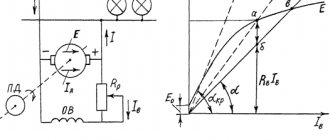
(Fig. 2.14).
In such diagrams, the voltage source Ek is usually not depicted.
In accordance with Kirchhoff's second law ik · Rk + uke− Ek = 0 From here we find the collector current ik: ik= − ( 1 / Rk ) · uke+ ( 1 / Rk ) · Ek which corresponds to a linear dependence of the form y = a · x + b. This equation describes the so-called load line (as for a circuit with a diode).
Let us depict the output characteristics of the transistor and the load line (Fig. 2.15).
In accordance with Kirchhoff’s second law, ib · Rb + ube − Ek = 0
From here we find the base current ib: ib = − ube / Rb + Ek / Rb
We will neglect the voltage ube since usually ube << Ek. Then ib = Ek / Rb
Thus, in the circuit under consideration, the current ib is set by the values of Ek and Rb (the current is “fixed”). In this case, ik= βst · ib + Íko
Let ib = ib2. Then the HPT will take the position shown in Fig. 2.15. It is easy to notice that the lowest possible position of the initial operating point corresponds to point Y (cut-off mode, ib = 0), and the highest position corresponds to point Z (saturation mode, ib > ib4).
A fixed base current circuit is rarely used for the following reasons:
- when exposed to destabilizing factors (for example, temperature), the values of βst and Íko change, which changes the current Ikn and the position of the initial operating point.
- for each value of βst, it is necessary to select the corresponding value of Rb, which is undesirable when using both discrete devices (i.e., devices not manufactured using integrated technology) and integrated circuits.
How does a transistor behave in different modes?
The transistor operates with variable or constant signals entering the input circuit.
Bipolar transistor: switching circuits, amplifier
For the most part, the transistor serves as an amplifier. An alternating signal at the input causes its output current to change. Here you can use schemes with OK or with OE. The signal requires a load in the output circuit. Typically a resistor is used in the output collector circuit. If it is chosen correctly, the output voltage will be significantly higher than the input.
The operation of the amplifier is clearly visible in the timing diagrams.
When pulse signals are converted, the mode remains the same as for sinusoidal ones. The quality of conversion of their harmonic components is determined by the frequency characteristics of the transistors.
Operation in switching mode
Transistor switches are designed for contactless switching of connections in electrical circuits. The principle is to change the resistance of the transistor in steps. The bipolar type is quite suitable for the requirements of the key device.