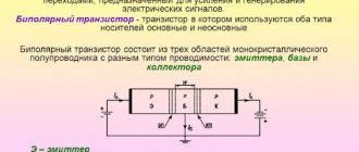
A bipolar transistor is an electronic semiconductor device, one of the types of transistors, designed to amplify, generate and convert electrical signals. The transistor is called bipolar because two types of charge carriers - electrons and holes - are simultaneously involved in the operation of the device. This differs from a unipolar (field-effect) transistor, in which only one type of charge carrier is involved.
The principle of operation of both types of transistors is similar to the operation of a water tap that regulates the flow of water, only a flow of electrons passes through the transistor. In bipolar transistors, two currents pass through the device - the main “large” current, and the control “small” current. The main current power depends on the control power. With field-effect transistors, only one current passes through the device, the power of which depends on the electromagnetic field. In this article we will take a closer look at the operation of a bipolar transistor.
Bipolar transistor design.
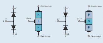
A bipolar transistor consists of three semiconductor layers and two PN junctions. PNP and NPN transistors are distinguished by the type of alternation of hole and electronic conductivity. It's like two diodes connected face to face or vice versa.
A bipolar transistor has three contacts (electrodes). The contact coming out of the central layer is called the base. The outermost electrodes are called collector and emitter. The base layer is very thin relative to the collector and emitter. In addition to this, the semiconductor regions at the edges of the transistor are asymmetrical. The semiconductor layer on the collector side is slightly thicker than on the emitter side. This is necessary for the transistor to operate correctly.
Connection schemes
To correctly use and connect BTs, you need to know their classification and type. Classification of bipolar transistors:
- Materials of manufacture: germanium, silicon and gallium arsenide.
- Manufacturing features.
- Power dissipation: low power (up to 0.25 W), medium (0.25-1.6 W), high power (above 1.6 W).
- Limit frequency: low-frequency (up to 2.7 MHz), mid-frequency (2.7-32 MHz), high-frequency (32-310 MHz), ultra-high-frequency (more than 310 MHz).
- Functional purpose.
The functional purpose of BT is divided into the following types:
- Low-frequency amplification with normalized and non-standardized noise figure (NiNNKSh).
- High-frequency amplification with NiNNKSh.
- Micro-frequency amplification with NiNNKSh.
- Powerful high-voltage amplifiers.
- Generator with high and ultra-high frequencies.
- Low-power and high-power high-voltage switching switches.
- Pulse powerful for working with high U values.
In addition, there are the following types of bipolar transistors:
- P-np.
- Npn.
There are 3 circuits for switching on a bipolar transistor, each of which has its own advantages and disadvantages:
- General B.
- General E.
- General K.
Operation of a bipolar transistor.
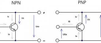
Let's consider the physical processes occurring during operation of a bipolar transistor. Let's take the NPN model as an example. The principle of operation of a PNP transistor is similar, only the polarity of the voltage between the collector and emitter will be opposite.
As already mentioned in the article about the types of conductivity in semiconductors, a P-type substance contains positively charged ions - holes. N-type substance is saturated with negatively charged electrons. In a transistor, the concentration of electrons in the N region significantly exceeds the concentration of holes in the P region.
Let's connect a voltage source between the collector and emitter VCE (VCE). Under its action, electrons from the upper N part will begin to be attracted to the plus and collect near the collector. However, current will not be able to flow because the electric field of the voltage source does not reach the emitter. This is prevented by a thick layer of collector semiconductor plus a layer of base semiconductor.
Now let's connect the voltage between the base and emitter VBE, but significantly lower than VCE (for silicon transistors the minimum required VBE is 0.6V). Since the layer P is very thin, plus a voltage source connected to the base, it will be able to “reach” with its electric field the N region of the emitter. Under its influence, electrons will be directed to the base. Some of them will begin to fill the holes located there (recombine). The other part will not find a free hole, because the concentration of holes in the base is much lower than the concentration of electrons in the emitter.
As a result, the central layer of the base is enriched with free electrons. Most of them will go towards the collector, since the voltage is much higher there. This is also facilitated by the very small thickness of the central layer. Some part of the electrons, although much smaller, will still flow towards the plus side of the base.
As a result, we get two currents: a small one - from the base to the emitter of the IBE, and a large one - from the collector to the emitter of the ICE.
If you increase the voltage at the base, then even more electrons will accumulate in the P layer. As a result, the base current will increase slightly and the collector current will increase significantly. Thus, with a small change in the base current IB, the collector current IC changes greatly. This is how the signal is amplified in a bipolar transistor . The ratio of the collector current IC to the base current IB is called the current gain. It is designated β, hfe or h21e, depending on the specifics of the calculations carried out with the transistor.
β = IC/IB
Step-by-step instructions for checking with a multimeter
Before starting the test, first of all, the structure of the triode device is determined, which is indicated by the emitter junction arrow. When the direction of the arrow points towards the base, then this is the PNP variant, the direction opposite to the base indicates NPN conductivity.
Testing a PNP transistor with a multimeter consists of the following sequential operations:
- We check the reverse resistance; to do this, we connect the “positive” probe of the device to its base.
- The emitter junction is tested; for this we connect the “negative” probe to the emitter.
- To check the collector, move the negative probe onto it.
The results of these measurements should show a resistance within the value of “1”.
To check direct resistance, swap the probes:
- We attach the “negative” probe of the device to the base.
- We alternately move the “positive” probe from the emitter to the collector.
- On the multimeter screen, the resistance readings should be from 500 to 1200 Ohms.
These readings indicate that the transitions are not broken, the transistor is technically sound.
Many amateurs have difficulty identifying the base, and, accordingly, the collector or emitter. Some advise starting to determine the base, regardless of the type of structure, in this way: alternately connecting the black probe of the multimeter to the first electrode, and the red probe alternately to the second and third.
The base will be detected when the voltage across the device begins to drop. This means that one of the transistor pairs has been found - “base-emitter” or “base-collector”. Next, you need to determine the location of the second pair in the same way. The common electrode of these pairs will be the base.
It will be interesting➡ Electrical engineering for dummies. How to learn to understand electrics: lessons for beginners
Verification methods
Any repair of electronics and electrical equipment begins with an external inspection, and then proceeds to measurements. This approach allows you to localize most faults. To find a varistor on the board, look at the figure below - this is what varistors look like. Sometimes they can be confused with capacitors, but can be distinguished by their markings.
If the element is burnt out and the markings cannot be read, look at this information on the device diagram. On the board and in the diagram it can be designated by the letters RU. The conventional graphic symbol looks like this.
There are three ways to test a varistor quickly and easily:
- Visual inspection.
- Call. This can be done with a multimeter or any other device that has a continuity test function.
- Resistance measurement. This can be done with a high-range ohmmeter, multimeter or megger.
A varistor fails when a large or prolonged current passes through it. Then the energy is dissipated in the form of heat, and if its amount is greater than that determined by the design, the element burns out. The housing of these components is made of a hard dielectric material, such as ceramic or epoxy coating. Therefore, when it fails, the integrity of the outer coating is most often damaged.
You can visually check the varistor for functionality - there should be no cracks on it, as in the photo:
The next method is to check the varistor with a tester in continuity mode. This cannot be done in the circuit, because the dialing can work through parallel-connected elements. Therefore, you need to unsolder at least one of its legs from the board.
Important: you should not check the elements for serviceability without desoldering them from the board - this may give false readings from the measuring instruments. Since in the normal state (without voltage applied to the terminals) the resistance of the varistor is high, it should not ring through. The test is performed in both directions, that is, by swapping the multimeter probes twice
The test is performed in both directions, that is, by swapping the multimeter probes twice
Since in the normal state (without voltage applied to the terminals) the resistance of the varistor is high, it should not ring through. The test is performed in both directions, that is, by swapping the multimeter probes twice.
On most multimeters, the continuity mode is combined with the diode testing mode. It can be found by the diode icon on the mode selector scale. If there is a sound indication sign next to it, it probably also has a dial tone.
Another way to test a varistor for breakdown with a multimeter is to measure the resistance. You need to set the device to the maximum measurement limit, in most devices this is 2 MOhms (megaohms, designated as 2M or 2000K). The resistance must be equal to infinity. In practice, it can be lower, within 1-2 MOhm.
Interesting! The same can be done with a megaohmmeter, but not everyone has one. It is worth noting that the voltage at the megohmmeter terminals should not exceed the classification voltage of the component being tested.
This ends the available methods for checking a varistor. This time, the multimeter will help the radio amateur find the faulty element, as in a large number of other cases. Although in practice a multimeter is not always needed in this matter, because the matter rarely goes beyond a visual inspection. Replace the burnt element with a new one, designed for voltage and with a diameter no less than the burnt one, otherwise it will burn out even faster than the previous one.
The simplest bipolar transistor amplifier
Let us consider in more detail the principle of signal amplification in the electrical plane using the example of a circuit. Let me make a reservation in advance that this scheme is not entirely correct. No one connects a DC voltage source directly to an AC source. But in this case, it will be easier and more clear to understand the amplification mechanism itself using a bipolar transistor. Also, the calculation technique itself in the example below is somewhat simplified.
1.Description of the main elements of the circuit
So, let’s say we have a transistor with a gain of 200 (β = 200). On the collector side, we will connect a relatively powerful 20V power source, due to the energy of which amplification will occur. From the base of the transistor we connect a weak 2V power source. We will connect to it in series an alternating voltage source in the form of a sine wave, with an oscillation amplitude of 0.1V. This will be a signal that needs to be amplified. The resistor Rb near the base is necessary in order to limit the current coming from the signal source, which usually has low power.
Calculation of base input current Ib
Now let's calculate the base current Ib. Since we are dealing with alternating voltage, we need to calculate two current values - at the maximum voltage (Vmax) and minimum (Vmin). Let's call these current values Ibmax and Ibmin, respectively.
Also, in order to calculate the base current, you need to know the base-emitter voltage VBE. There is one PN junction between the base and emitter. It turns out that the base current “meets” the semiconductor diode on its path. The voltage at which a semiconductor diode begins to conduct is about 0.6V. We will not go into details of the current-voltage characteristics of the diode, and for simplicity of calculations we will take an approximate model, according to which the voltage on the current-carrying diode is always 0.6V. This means that the voltage between base and emitter VBE = 0.6V. And since the emitter is connected to ground (VE = 0), the voltage from base to ground is also 0.6V (VB = 0.6V).
Let's calculate Ibmax and Ibmin using Ohm's law:
Calculation of collector output current IC
Now, knowing the gain (β = 200), you can easily calculate the maximum and minimum values of the collector current (Icmax and Icmin).
Calculation of output voltage Vout
It remains to calculate the voltage at the output of our amplifier Vout. In this circuit, this is the voltage at the collector VC.
The collector current flows through the resistor Rc, which we have already calculated. It remains to substitute the values:
Analysis of results
As can be seen from the results, VCmax turned out to be less than VCmin. This is because the voltage across resistor VRc is subtracted from the supply voltage VCC. However, in most cases this does not matter, since we are interested in the variable component of the signal - the amplitude, which has increased from 0.1V to 1V. The frequency and sinusoidal shape of the signal have not changed. Of course, a Vout/Vin ratio of ten times is far from the best indicator for an amplifier, but it is quite suitable for illustrating the amplification process.
So, let's summarize the principle of operation of an amplifier based on a bipolar transistor. A current Ib flows through the base, carrying DC and AC components. A constant component is needed so that the PN junction between the base and emitter begins to conduct - “opens”. The variable component is, in fact, the signal itself (useful information). The collector-emitter current inside the transistor is the result of the base current multiplied by the gain β. In turn, the voltage across the resistor Rc above the collector is the result of multiplying the amplified collector current by the resistor value.
Thus, the Vout pin receives a signal with an increased oscillation amplitude, but with the same shape and frequency. It is important to emphasize that the transistor takes energy for amplification from the VCC power source. If the supply voltage is insufficient, the transistor will not be able to operate fully, and the output signal may be distorted.
Transistor pairs in amplifier stages
You may be wondering what is the reason to use PNP transistors when there are many NPN transistors available that can be used as amplifiers or solid state switches? However, having two different types of transistors—NPN and PNP—provides great advantages when designing power amplifier circuits. These amplifiers use “complementary” or “matched” pairs of transistors (representing one PNP transistor and one NPN transistor connected together, as shown in the figure below) in the output stage.
Two corresponding NPN and PNP transistors with similar characteristics, identical to each other, are called complementary. For example, TIP3055 (NPN type) and TIP2955 (PNP type) are a good example of complementary silicon power transistors. They both have DC current gain β=IC/IB matched within 10% and high collector current of around 15A, making them ideal for motor control or robotic applications.
In addition, class B amplifiers use matched pairs of transistors in their output power stages. In them, the NPN transistor conducts only the positive half-wave of the signal, and the PNP transistor only conducts its negative half.
This allows the amplifier to pass the required power through the speaker in both directions at a given power rating and impedance. As a result, the output current, which is usually on the order of several amperes, is evenly distributed between the two complementary transistors.
Operating modes of a bipolar transistor
In accordance with the voltage levels on the electrodes of the transistor, there are four modes of its operation:
- Cut off mode.
- Active mode.
- Saturation mode.
- Inverse mode (reverse mode).
Cut-off mode
When the base-emitter voltage is lower than 0.6V - 0.7V, the PN junction between the base and emitter is closed. In this state, the transistor has no base current. As a result, there will be no collector current either, since there are no free electrons in the base ready to move towards the collector voltage. It turns out that the transistor is, as it were, locked, and they say that it is in cutoff mode.
Active mode
In active mode, the voltage at the base is sufficient for the PN junction between the base and emitter to open. In this state, the transistor has base and collector currents. The collector current equals the base current multiplied by the gain. That is, the active mode is the normal operating mode of the transistor, which is used for amplification.
Saturation mode
Sometimes the base current may be too high. As a result, the supply power is simply not enough to provide such a magnitude of collector current that would correspond to the gain of the transistor. In saturation mode, the collector current will be the maximum that the power supply can provide and will not depend on the base current. In this state, the transistor is not able to amplify the signal, since the collector current does not respond to changes in the base current.
In saturation mode, the conductivity of the transistor is maximum, and it is more suitable for the function of a switch (switch) in the “on” state. Similarly, in the cut-off mode, the conductivity of the transistor is minimal, and this corresponds to the switch in the off state.
Inverse mode
In this mode, the collector and emitter change roles: the collector PN junction is biased in the forward direction, and the emitter junction is biased in the opposite direction. As a result, current flows from the base to the collector. The collector semiconductor region is asymmetrical to the emitter, and the gain in inverse mode is lower than in normal active mode. The transistor is designed in such a way that it operates as efficiently as possible in active mode. Therefore, the transistor is practically not used in inverse mode.
Advantages
- The device has high amplification capacity.
- It demonstrates high-quality performance at high frequencies.
- The device has the best voltage amplification.
- It can operate at both low and high power.
- Has a high current density.
- Has a low forward voltage drop.