The principle of semiconductor control of electric current was known at the beginning of the twentieth century. Even though electronics engineers knew how a transistor worked, they continued to design devices based on vacuum tubes. The reason for such distrust of semiconductor triodes was the imperfection of the first point-point transistors. The family of germanium transistors did not have stable characteristics and were highly dependent on temperature conditions.
Monolithic silicon transistors began to seriously compete with vacuum tubes only in the late 50s. Since that time, the electronics industry began to develop rapidly, and compact semiconductor triodes actively replaced energy-intensive lamps from electronic device circuits. With the advent of integrated circuits, where the number of transistors can reach billions, semiconductor electronics has won a landslide victory in the fight to miniaturize devices.
What is a bipolar transistor
Transistors can be thought of as switches of sorts, just like many electronic components such as relays or vacuum tubes.
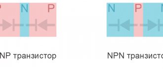
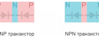
Transistors are used in various circuits, and rarely is a circuit complete without them, even now with the widespread use of microcircuits. There are two main types of bipolar transistors - npn and pnp, they differ in conductivity. Two similar transistors of different conductivities are called a complementary pair. If in some circuit, for example, in an amplifier, you replace transistors of one type with transistors of another type with similar parameters (not forgetting to change the polarity of the supply voltages, electrolytic capacitors and semiconductor diodes), then the circuit will work exactly the same, with the exception Microwave range, since npn transistors are higher frequency than pnp, and here it may not be possible to select a complementary pair.
A bipolar transistor is a three-electrode semiconductor device, a type of transistor. The electrodes are connected to three successively arranged semiconductor layers with alternating types of impurity conductivity.
Most often, transistors of the NPN structure are used in circuits. This is due to the fact that in the circuits the emitters of the transistors are connected to a negative power supply.
Accordingly, the common wire of the circuit will also be connected to the negative terminal of the power supply, which is a generally accepted standard.
Transistors are available in various cases, but they all have three terminals (high-frequency transistors sometimes have a fourth terminal connected to a metal case - a screen):
- The base is the control output;
- The collector is under positive potential (for an NPN transistor);
- The emitter is at negative potential (for an NPN transistor).
What determines the power of the circuit?
This scheme has limitations. You can change VT1 KT315 to a more powerful one, which will have a higher gain, but this gain limit is not infinite.
First of all, it all depends on the transistor used. If you change it to a more powerful one, then the gain will be higher. But it should be remembered that the more powerful the transistor, the more powerful the input signal is needed. In addition, you will have to recalculate all components. And connect the preamplifier, assemble the power supply circuit, and this will be a completely different circuit.
Transistors have a number of parameters that affect the circuit. This is the gain for current (h21e), voltage, power. Another important parameter is the power dissipation on the collector. As power increases, a radiator will be required to remove heat.
Bipolar transistor device
According to standard circuits, the letter “B” is called “Base” - the inner layer of the device, its foundation, which leads to the conversion or change of the current signal. The arrow in the circle shows the movement of current charges in “E”.
“E” - “Emitter” - the internal main component of the transistor, designed to transfer charged elementary particles to “B”.
“K” - “Collector” is the second component of the transistor device, which collects the same charges that pass through “B”.
The “Base” layer is structurally very thin due to the recombination of charged particles that go through the base layer with the constituent particles of this layer. At the same time, the “Collector” layer is designed as wide as possible for high-quality collection of charges.
Types of bipolar transistors
Bipolar transistors are classified into the following types: 1. Based on the source material - germanium or silicon. 2. According to production technology - alloy, epitaxial-planar, conversion, etc. 3. According to the mechanism of movement of charge carriers - drift and diffusion. 4. By power dissipation - low power (up to 0.3 W), medium power (from 0.3 to 3 W) and high power (more than 3 W). 5. According to the range of operating frequencies - low frequency (up to 3 MHz), medium (from 3 to 30 MHz), high (from 30 to 300 MHz), ultra-high frequency (more than 300 MHz).
The principle of operation of a bipolar transistor
Now we will try to figure out how a transistor works. I will not go into details of the internal structure of transistors as this information will only confuse. Better take a look at this drawing.
This image best explains the working principle of a transistor. In this image, a person controls the collector current using a rheostat. He looks at the base current; if the base current increases, then the person also increases the collector current, taking into account the gain of the transistor h21E. If the base current drops, then the collector current will also decrease - the person will correct it using a rheostat.
This analogy has nothing to do with the actual operation of a transistor, but it makes it easier to understand the principles of its operation.
For transistors, rules can be noted to help make things easier to understand. (These rules are taken from the book “The Art of Circuit Design” by P. Horowitz W. Hill).
- The collector has a more positive potential than the emitter
- As I already said, the base-collector and base-emitter circuits work like diodes
- Each transistor is characterized by limiting values such as collector current, base current and collector-emitter voltage.
- If rules 1-3 are followed, then the collector current Ik is directly proportional to the base current Ib. This relationship can be written as a formula.
From this formula we can express the main property of a transistor - a small base current controls a large collector current.
- current gain.
It is also denoted as
Based on the above, the transistor can operate in four modes:
- Transistor cutoff mode - in this mode, the base-emitter junction is closed, this can happen when the base-emitter voltage is insufficient. As a result, there is no base current and therefore there will be no collector current either.
- The active mode of a transistor is the normal mode of operation of the transistor. In this mode, the base-emitter voltage is sufficient to cause the base-emitter junction to open. The base current is sufficient and the collector current is also available. The collector current is equal to the base current multiplied by the gain.
- Transistor saturation mode - the transistor enters this mode when the base current becomes so large that the power of the power source is simply not enough to further increase the collector current. In this mode, the collector current cannot increase following an increase in the base current.
- Inverse transistor mode - this mode is used extremely rarely. In this mode, the collector and emitter of the transistor are swapped. As a result of such manipulations, the gain of the transistor suffers greatly. The transistor was not originally designed to operate in such a special mode.
To understand how a transistor works, you need to look at specific circuit examples, so let's look at some of them.
Transistor in switch mode
A transistor in switch mode is one of the cases of transistor circuits with a common emitter. The transistor circuit in switching mode is used very often. This transistor circuit is used, for example, when it is necessary to control a powerful load using a microcontroller. The controller leg is not capable of pulling a powerful load, but the transistor can. It turns out that the controller controls the transistor, and the transistor controls a powerful load. Well, first things first.
The main idea of this mode is that the base current controls the collector current. Moreover, the collector current is much greater than the base current. Here you can see with the naked eye that the current signal is amplified. This amplification is carried out using the energy of the power source.
Recommended reading: Stepper motor control
The figure shows a diagram of the operation of a transistor in switching mode.
For transistor circuits, voltages do not play a big role, only currents matter. Therefore, if the ratio of the collector current to the base current is less than the gain of the transistor, then everything is okay.
In this case, even if we have a voltage of 5 volts applied to the base and 500 volts in the collector circuit, then nothing bad will happen, the transistor will obediently switch the high-voltage load.
The main thing is that these voltages do not exceed the limit values for a specific transistor (set in the transistor characteristics).
Well, now let's try to calculate the value of the base resistor.
As far as we know, the current value is a characteristic of the load.
Those. I=U/R
We don't know the resistance of the light bulb, but we know the operating current of the light bulb is 100 mA. In order for the transistor to open and allow such current to flow, you need to select the appropriate base current. We can adjust the base current by changing the value of the base resistor.
Since the minimum value of the transistor gain is 10, then for the transistor to open, the base current must become 10 mA.
The current we need is known. The voltage across the base resistor will be This voltage value across the resistor is due to the fact that 0.6V-0.7V is dropped at the base-emitter junction and we must not forget to take this into account.
As a result, we can easily find the resistance of the resistor
All that remains is to choose a specific value from a number of resistors and it’s done.
Now you probably think that the transistor switch will work as it should? That when the base resistor is connected to +5 V the light bulb lights up, when it is turned off the light bulb goes out? The answer may or may not be yes.
The thing is that there is a small nuance here.
The light bulb will go out when the resistor potential is equal to the ground potential. If the resistor is simply disconnected from the voltage source, then everything is not so simple. The voltage on the base resistor can miraculously arise as a result of interference or some other otherworldly evil spirit
To prevent this effect from happening, do the following. Another resistor Rbe is connected between the base and emitter. This resistor is chosen with a value at least 10 times larger than the base resistor Rb (In our case, we took a 4.3 kOhm resistor).
When the base is connected to any voltage, the transistor works as it should, the resistor Rbe does not interfere with it. This resistor consumes only a small portion of the base current.
In the case when voltage is not applied to the base, the base is pulled up to the ground potential, which saves us from all kinds of interference.
So, in principle, we have figured out the operation of the transistor in the key mode, and as you can see, the key mode of operation is a kind of voltage amplification of the signal. After all, we controlled a voltage of 12 V using a low voltage of 5V.
Emitter follower
An emitter follower is a special case of common-collector transistor circuits.
A distinctive feature of a circuit with a common collector from a circuit with a common emitter (option with a transistor switch) is that this circuit does not amplify the voltage signal. What went in through the base came out through the emitter, with the same voltage.
Indeed, let’s say we applied 10 volts to the base, while we know that at the base-emitter junction somewhere around 0.6-0.7V is dropped. It turns out that at the output (at the emitter, at the load Rн) there will be a base voltage of minus 0.6V.
It turned out 9.4V, in a word, almost as much as went in and out. We made sure that this circuit will not increase the voltage for us.
“What is the point then of turning on the transistor like this?” you ask. But it turns out that this scheme has another very important property. The circuit for connecting a transistor with a common collector amplifies the signal in terms of power. Power is the product of current and voltage, but since the voltage does not change, the power increases only due to the current! The load current is the sum of the base current plus the collector current. But if you compare the base current and the collector current, the base current is very small compared to the collector current. It turns out that the load current is equal to the collector current. And the result is this formula.
Now I think it’s clear what the essence of the emitter follower circuit is, but that’s not all.
The emitter follower has another very valuable quality - high input impedance. This means that this transistor circuit consumes almost no input current and creates no load on the signal source circuit.
To understand the principle of operation of a transistor, these two transistor circuits will be quite sufficient. And if you experiment with a soldering iron in your hands, the epiphany simply won’t keep you waiting, because theory is theory, and practice and personal experience are hundreds of times more valuable!
Collector power
Collector power circuits
contain the elements shown below.
In multistage amplifiers, the collector circuits of all stages are connected in parallel to one common source E0C. In this case, the collector power circuit contains an RfSf decoupling filter. The purpose of such a filter is to eliminate parasitic feedback through a common power source. When powered from an alternating current network, the supply voltage ripple is also reduced. Resistor Rф is connected in series with the load RN, and part of the collector voltage is lost on it. Therefore, it is recommended to select resistance Rf based on the permissible voltage drop:
The voltage between the collector and emitter of the UCE transistor is selected within the range
In this case, the minimum value of UC should not be less than 0.5 V, otherwise the operating point goes into the saturation region and nonlinear distortion increases.
Advantages and disadvantages of bipolar transistors
The advantages of bipolar transistors in comparison with analogues include:
- control of electrical charges;
- reliability in operation;
- resistance to frequency interference;
- low noise characteristics;
The disadvantages include:
- has a low input resistance, due to which the signal amplification characteristics deteriorate;
- severe sensitivity to static charges;
- the connection diagram assumes the presence of 2 power supplies;
- At high temperatures the transistor may be damaged.
How to assemble a circuit
The circuit can be assembled on a PCB or on a breadboard. Follow the link to this article, it describes in more detail the process of assembling and testing the circuit.
Use quality parts and good solder. She's working. This is generally a classic circuit for connecting a bipolar transistor with a common emitter.
Also on the site there are other amplifier circuits that are not difficult to assemble and not expensive in terms of the cost of parts.
How to test a bipolar transistor
Since a bipolar transistor consists of two pn junctions, checking it with a digital tester is quite simple.
It is necessary to set the tester operation switch to the diode test position, connecting one probe to the base, and the second - alternately to the emitter and collector.
Essentially, we are simply sequentially checking the health of the pn junctions.
Such a transition can be either open or closed.
Then you need to change the polarity of the probes and repeat the measurements.
In one case, the tester will show a voltage drop at the emitter-base and collector-base junctions of 0.6 - 0.7 V (both junctions are open).
In the second case, both transitions will be closed, and the tester will record this.
It should be noted that in operating mode, most often one of the transitions of the transistor is open and the second is closed.
Stabilization of the circuit operation
When a semiconductor heats up, its resistance decreases. The transistor is made of a semiconductor, and accordingly its pn junctions are too.
When the ULF circuit operates, current flows through the transistor and it heats up. Typically all power is dissipated at the collector. Nevertheless, the characteristics of the transistor change dramatically, since the resistance of its pn junction decreases sharply as the temperature rises.
To stabilize the operation of the transistor, you need to balance its resistance with another source. This can be done using additional resistance.
When the resistance of transistor VT1 decreases, resistor R3 takes part of the voltage onto itself and does not allow the current in the circuit to increase.
Thanks to this, the transistor:
- does not close;
- does not go into saturation mode;
- does not distort the signal;
- and doesn't overheat.
This is called thermal stabilization of the amplifier.
And so that in normal operation, when VT1 does not heat up, resistor R3 does not reduce the power of the circuit, a shunt electrolytic capacitor C2 is included in the circuit. The variable component of the input signal passes through it without loss.
Measuring the current gain of a bipolar transistor
If the tester has the ability to measure the current transfer coefficient, then you can check the operation of the transistor by installing the transistor leads into the corresponding sockets.
We recommend reading: Voltage rectifier: operating principle and types
Current transfer coefficient is the ratio of the collector current to the base current.
The higher the gain, the more collector current can be controlled by the base current, all other things being equal.
The pinout (pin name) and other data can be taken from the data sheets (reference data) for the corresponding transistor. Data sheets can be found on the Internet through search engines.
The tester will show on the display the current transfer (gain) coefficient, which must be compared with the reference data.
The current transfer coefficient of low-power transistors can reach several hundred.
For powerful transistors it is significantly smaller - several units or tens.
However, there are powerful transistors with a transfer coefficient of several hundred or thousand. These are the so-called Darlington pairs.
A Darlington pair consists of two transistors. The output current of the first transistor is the input current for the second.
The overall current transfer coefficient is the product of the coefficients of the first and second transistors.
The Darlington pair is made in a common housing, but it can also be made from two separate transistors.
Amplifier output
At the output of the amplifier, you can connect either another amplifier, which will amplify the signal even more, or a dynamic head. The dynamic head is a regular speaker. It will reproduce the sound from the output of transistor VT1.
However, there are many nuances here too.
The most important thing concerns the matching of the load resistance and the amplifier resistance.
If the output resistance of the transistor is much greater than that of the dynamic head, then it will not be able to transmit all the power. At a minimum, most of the voltage will remain on its contacts.
This circuit requires a speaker with a resistance of about 1 kOhm.
If you set it less, for example, by 4 Ohms, then even half the power will not be reproduced, and the VT1 collector will begin to heat up even more.
The matching of the input, output and amplifier load resistances is calculated at the circuit design stage. Therefore, they should not be violated.
Built-in diode protection
Some transistors (power and high voltage) can be protected from reverse voltage by a built-in diode.
Thus, if you connect the tester probes to the emitter and collector in diode testing mode, it will show the same 0.6 - 0.7 V (if the diode is forward biased) or a “blocked diode” (if the diode is reverse biased) .
If the tester shows some small voltage, and in both directions, then the transistor is definitely broken and must be replaced. A short can also be determined in resistance measurement mode - the tester will show low resistance.
There is (fortunately, quite rarely) a “mean” malfunction of transistors. This is when it works at first, but after some time (or after warming up) it changes its parameters or fails altogether.
If you unsolder such a transistor and check it with a tester, it will have time to cool before the probes are connected, and the tester will show that it is normal. The best way to verify this is by replacing the “suspicious” transistor in the device.
In conclusion, let’s say that the bipolar transistor is one of the main “pieces of hardware” in electronics. It would be nice to learn to find out whether these “pieces of iron” are “alive” or not. Of course, I have given you, dear readers, a very simplified picture.
In fact, the operation of a bipolar transistor is described by many formulas, there are many varieties of them, but it is a complex science. For those wishing to dig deeper, I can recommend the wonderful book by Horowitz and Hill, “The Art of Circuit Design.”
Bipolar transistor connection circuits
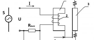
A bipolar transistor has three terminals: emitter, collector and base. A signal comes to two of them, and from the other two it is removed, because one of them is common for entry and exit. So, which electrode is connected to the common bus, so is the connection diagram: with a common emitter (CE), a common base (CB) or a common collector (CC).
a) The connection circuit for a bipolar transistor with an OE is used most often in practice. In the above circuit, the input signal is supplied between the base and emitter through a decoupling capacitor Cp in order to cut off the DC voltage from the previous stage and not affect the power supply to the next stage. The amplified alternating voltage is removed from the collector and common terminal. This connection circuit provides both current and voltage gain. Such a connection will have a high output resistance (up to tens of kiloohms and depends on the value of Rk), but a low input resistance (500-1000 Ohms).
b) The following diagram shows switching on with OK. The bipolar transistor in this case works as a current amplifier and the voltage values at the input and output are almost the same. A feature of this connection is the high input resistance (from 10 kOhm to 500 kOhm), which provides good matching with the signal source stage. Also, the phase of the output voltage coincides with the phase of the input (there is no “flip” of the output signal, as in a circuit with an OE). Therefore, such a connection is called an emitter follower. But its output resistance is low, which greatly depends on the load resistance Re.
c) In the circuit with OB, we “ground” the base to the common wire through the capacitor Sat. In this case, the transistor only amplifies voltage, but there is no current amplification. Its input resistance is small (tens of ohms), and such a connection is used mainly in generators.
Connection diagram with a common base.
This circuit is very good when using high frequency signals. In principle, this is what switching on the transistor is used for in the first place. Very big disadvantages are the low input resistance and, of course, the lack of current amplification. See for yourself, at the input we have the emitter current I_e, at the output I_k.
I_e = I_k + I_b
That is, the emitter current is greater than the collector current by a small amount of the base current. This means that there is not just no current gain, moreover, the output current is slightly less than the input current. Although, on the other hand, this circuit has a fairly large voltage transfer coefficient. These are the advantages and disadvantages, let’s continue...
Connection diagram for a bipolar transistor with a common collector
This is what the wiring diagram for a bipolar transistor with a common collector looks like. Doesn't remind you of anything? If we look at the circuit from a slightly different angle, we will recognize our old friend here - the emitter follower. There was almost a whole article about it (here it is), so we have already covered everything related to this scheme. Meanwhile, we are waiting for the most commonly used circuit - with a common emitter.
Connection circuit for a bipolar transistor with a common emitter.
This circuit has earned popularity for its amplifying properties. Of all the circuits, it gives the greatest gain in current and voltage; accordingly, the increase in signal power is also large. The disadvantage of the circuit is that the amplification properties are strongly influenced by increasing temperature and signal frequency.
We got acquainted with all the circuits, now let’s take a closer look at the last (but not the least important) amplifier circuit based on a bipolar transistor (with a common emitter). First, let's depict it a little differently:
There is one minus here - the grounded emitter. When the transistor is turned on in this way, there are nonlinear distortions at the output, which, of course, must be combated. Nonlinearity occurs due to the influence of the input voltage on the emitter-base junction voltage. Indeed, there is nothing “extra” in the emitter circuit; the entire input voltage turns out to be applied precisely to the base-emitter junction. To cope with this phenomenon, we add a resistor to the emitter circuit. So we will receive negative feedback.
We recommend reading: How to measure resistance with a multimeter: instructions, photos, videos
What is this?
In short, the principle of negative feedback is that some part of the output voltage is transferred to the input and subtracted from the input signal. Naturally, this leads to a decrease in the gain, since the input of the transistor, due to the influence of feedback, will receive a lower voltage value than in the absence of feedback.
Nevertheless, negative feedback is very useful for us. Let's see how it will help reduce the influence of the input voltage on the voltage between the base and emitter.
So, even if there is no feedback, an increase in the input signal by 0.5 V leads to the same increase in U_{be}. Everything is clear here. Now let’s add feedback! And in the same way we increase the input voltage by 0.5 V. Following this, U_{be} increases, which leads to an increase in the emitter current. And an increase in I_e leads to an increase in the voltage across the feedback resistor. It would seem, what's wrong with this? But this voltage is subtracted from the input! Look what happened:
The input voltage has increased - the emitter current has increased - the voltage across the negative feedback resistor has increased - the input voltage has decreased (due to the subtraction of U_{os}) - the voltage U_{be} has decreased.
That is, negative feedback prevents the base-emitter voltage from changing when the input signal changes. As a result, our amplifier circuit with a common emitter was supplemented with a resistor in the emitter circuit:
There is another problem with our amplifier. If a negative voltage value appears at the input, the transistor will immediately close (the base voltage will become less than the emitter voltage and the base-emitter diode will close), and nothing will happen at the output. This is somehow not very good... Therefore, it is necessary to create an offset. This can be done using a divisor as follows:
We got such a beauty. If resistors R_1 and R_2 are equal, then the voltage on each of them will be equal to 6V (12V / 2). Thus, in the absence of a signal at the input, the base potential will be +6V. If a negative value, for example -4V, comes to the input, then the base potential will be equal to +2V, that is, the value is positive and does not interfere with the normal operation of the transistor.
How else can we improve our circuit... Let us know what signal we will amplify, that is, we know its parameters, in particular the frequency. It would be great if there was nothing at the input except the useful amplified signal. How to ensure this? Of course, with the help of a high-pass filter! Let's add a capacitor, which in combination with a bias resistor forms a high-pass filter:
This is how the circuit, in which there was almost nothing except the transistor itself, was overgrown with additional elements. Perhaps we’ll stop there; soon there will be an article devoted to the practical calculation of an amplifier based on a bipolar transistor. In it we will not only draw up a circuit diagram of the amplifier, but also calculate the ratings of all elements, and at the same time select a transistor suitable for our purposes. See you soon!
Input characteristics for a common emitter circuit.
Let us depict the characteristics of the already considered transistor KT603A (Fig. 1.60).
Now the Earley effect manifests itself in the fact that as the voltage uke increases, the characteristics shift to the right. The differential resistance is now determined by the expression rdif= (dube/dib) |ib– given, uke= const
Output characteristics for a common emitter circuit
Let us depict these characteristics for the KT603A transistor (Fig. 1.61).
Let us turn to the previously obtained expression ik=αst·ie+iko In accordance with Kirchhoff's first law ie=ic+ib and taking into account the previous expression we obtain ikαst· (ic+ib) +icо from where ik=αst/ (1 -αst) ·ib + 1 / (1 -αst) iko
Let us introduce the notation: βst ≡ αst / (1- αst )
The coefficient αst is called the static transfer coefficient of the base current. Its value is usually tens - hundreds (this is a dimensionless coefficient).
It is easy to see that 1 / (1 -αst) = βst + 1 Let us introduce the designation i′ko ≡ (βst + 1) ·iko As a result, we obtain iк= βst ·ib+i′ko This expression, to a first approximation, describes the output characteristics in the active region work without taking into account the slope of the characteristics.
To take into account the slope, the expression is written in the form ik= βst ·ib+i′ko +ukb· ( 1 /r′к), where r′к =duke/dik|uke – given, ib=const
To a first approximation, r′k = ( 1 / 1 + βst) · rk (resistance rk is defined above). The so-called differential base current transfer coefficient β is often used.
To increase the collector current ∆iк and base current ∆ib, we can write:
∆iк ≈ β ∆ iб
By definition β=diк/diб|iк – given, uke=const
For the KT603A transistor at t = 25°C β = 10...80.
The value of β depends on the operating mode of the transistor. Let us present a typical graph of the dependence of β on the emitter current (it is almost equal to the collector current) for ukb = 2 V (Fig. 1.62).
For normal operation of the transistor at direct current, in addition to the condition Pk < Pk max discussed above, the conditions ik must be met
For the KT603A transistor discussed above, ik max = 300 mA, uke max = 30 V (at t < 70 ° C).
Let us schematically depict on the output characteristics for a circuit with a common emitter the so-called safe operation area in which the specified conditions are met (Fig. 1.63).
It is usually acceptable to assume (with some error) that the output characteristics for a circuit with a common emitter are located on straight segments fan-shaped from one point on the voltage axis (Fig. 1.64).
The voltage Ue (this is a positive value) is called the Early voltage. For transistor KT603A Ue ~ 40 V.
Amplifier input
The amplifier input is terminals X1 and X2.
X2 is the minus of the input, and X1 is the plus. Since the circuit is for one channel, the ULF is called mono.
You can connect both the left and right channels, or both at once.
Input filtering
Electrolytic capacitor C1 allows you to separate the DC component of the incoming signal from the variable one.
Simply put, it only passes the AC signal. If there is no signal, or the amplifier input is short-circuited, then without this capacitor the transistor may go into saturation mode (maximum gain), and an unpleasant wheeze will appear at the output.
Do not confuse this effect with whistling. The whistle is the influence of positive feedback, and in this case there will be a saturation mode due to a short circuit at the input. And at the output of the amplifier, it is the wheezing that will be heard, and not the sound or sound.
The capacitance of the capacitor is matched to the frequency of the sound signal. The sound starts from 20 Hz and up to 16 kHz.