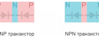
Bipolar transistor
A semiconductor device consists of three layers of different conductivity, each of which is connected to conductive contacts.
The collector, base and emitter layers differ little in the degree of electrical conductivity, but during production they are subject to different levels of doping:
- The first is lightly doped, which makes it possible to increase the collector voltage.
- Many impurities are added to the emitter during manufacturing. The amount of reverse breakdown voltage does not become critical, since the devices operate with a forward-biased junction. Increased doping results in increased injection of secondary charge carriers into the base layer.
The base layer is lightly doped, since it is located between the collector and the emitter, this layer should show high resistance.
How does it work
Charge carriers move to the collector through a thin base layer. The middle layer is separated from the upper and lower pn junctions.
Features of operation:
- Current flows through the transistor if charging carriers are injected through the pn junction into the base layer from the emitter layer.
- The result is a reduction in potential obstruction when applying forward bias.
- In the base layer, the injected charges are not the majority carriers, therefore they are accelerated and enter other pn junctions to the collector layer from the base layer.
- In the base, charges spread under the influence of diffusion or electric field.
Transistor efficiency improves if a thin base layer is used, but excessive thinning reduces the collector voltage limit.
Connection diagram
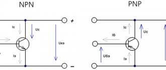
The transistor has three terminals for installation in a circuit. When connected, one contact is defined as common.
There are connection schemes:
- With joint emitter. A commonly used circuit amplifies the current and voltage (showing the greatest power increase). The input pulse arrives at the base layer from the emitter side, is removed from the collector and is inverted.
- With a joint collector. Only the electric current increases, the voltage gain is 1, the input resistance is high and the output resistance is low. The connection supports a wide range of amplified frequencies.
If the base layer is common when connected, the voltage increases, so it is used more often in composite systems, but not in single-transistor ones.
Literature on electronics
The science that studies transistors and other devices is called electronics. Its entire section is devoted to semiconductor devices. If you are interested in getting more information about the operation of transistors, you can read the following books on this topic:
- Digital Circuit Design and Computer Architecture - David M.
- OS. Design and implementation - Andrew T.
- Power electronics for amateurs and professionals - B. Yu. Semenov.
These books describe various programmable electronics tools. Of course, all programmable circuits are based on transistors. Thanks to these books, you will not only gain new knowledge about transistors, but also skills that may bring you income.
Now you know how transistors work and where they are used in life. If you are interested in this topic, continue to study it, because progress does not stand still, and all technical devices are constantly being improved. In this matter, it is very important to keep up with the times. I wish you success!
Sources
- https://habr.com/ru/post/133136/
- https://principraboty.ru/princip-raboty-tranzistora/
- https://odinelectric.ru/knowledgebase/kak-rabotaet-tranzistor-i-gde-ispolzuetsya
- https://rusenergetics.ru/oborudovanie/skhema-tranzistora
- https://RadioStorage.net/1670-tranzistory-osnovnye-parametry-i-harakteristiki-markirovka-tranzistorov.html
- https://tokar.guru/hochu-vse-znat/tranzistor-vidy-primenenie-i-principy-raboty.html
- https://www.RusElectronic.com/chitaem-elektricheskie-skhemi-s-tranzistorami/
Did the article help you?
Field-effect transistor
The purpose is the same as bipolar, but the structure is different. Transistors coordinate higher powers in similar sizes.
The structure contains elements:
- drain for receiving high voltage;
- gate for controlled voltage;
- source for distributing voltage in the open position.
Valera
The voice of the construction guru
Ask a Question
There are field-type devices: with control via a pn junction, with an electrically insulated gate. In the first case, on opposite sides of the semiconductor, areas of different electrical conductivity are obtained to control the electric current. In the second type, the gate is separated from the channel by a dielectric material.
How does it work
In a field-effect device, current flows to the drain through a channel in the doped conductor under the gate. It is located between the undoped layer (there are no charging carriers in it) and the gate. There is a depletion region here where no current is conducted.
The width of the channel is limited by the area between the depletion region and the interlayer. The current is controlled by changing the voltage applied to the gate. In this case, the channel cross-section changes, and the output current changes its value.
Connection schemes
Field-effect transistors are connected in one of three ways:
- with common drain;
- with a common source;
- with a common base.
The circuit with a common drain is similar to connecting a bipolar module with a common collector. This type of connection is used in matching cascades, where a high input voltage is needed and a low output voltage. The inclusion supports a wide range of frequencies.
The common source circuit produces a large increase in power and current, while the phase of the drain circuit voltage is reversed. The input resistance can be several hundred megaohms; to reduce it, a resistor is added between the source and gate.
In a circuit with a common gate, there is no amplification of the electric current, the increase in power is small. The voltage is in a similar phase with the control one. When the input pulse changes, the voltage at the source increases or decreases.
Color and digital marking
Transistors, like other radio components, are marked using a color code. The color code consists of images of geometric shapes (triangles, squares, rectangles, etc.), colored dots and Latin letters.
The code is applied to the flat parts, cover and other places of the transistor. From it you can find out the type of transistor, month and year of manufacture. Marking locations and color codes for some types of transistors are shown in Fig. 2…3 and in table. 1…4. It is also practiced to mark some types of transistors with a digital code (Table 4).
Table 1. Color and code markings of low-power mid-frequency and high-frequency transistors.
| Transistor type | Transistor groups | Release month | Year of issue | ||||
| Designation | Marking | Designation | Marking | Designation | Marking | Designation | Marking |
| yang v. | beige | ||||||
| A | pink | Feb. | blue | 1977 | beige | ||
| B | yellow | March | green | 1978 | ealate | ||
| IN | blue | Apr. | red | 1979 | orange | ||
| G | beige | May | ealate | 1980 | electrician | ||
| D | orange | June | gray | 1981 | turquoise | ||
| KT3107 | blue | E | electrician | July | brown | 1982 | white |
| AND | ealate | Aug. | orange | 1983 | red | ||
| AND | green | Sep. | electrician | 1984 | brown | ||
| TO | red | Oct. | white | 1985 | green | ||
| L | gray | November | yellow | 1986 | blue | ||
| December | blue | ||||||
Table 2. Color marking of transistor KT3107.
Rice. 2. Places for color and code marking of low-power mid-frequency and high-frequency transistors in the KT-26 (TO-92) housing.
Rice. 3. Places of color marking of the KT3107 transistor in the KT-26 (TO-92) housing.
Rice. 4. Places of code marking of transistors in the KT-27 (TO-126) housing.
Table 3. Color and code markings of transistors.
| Code | Type |
| 4 | KT814 |
| 5 | KT815 |
| 6 | KT816 |
| 7 | KT817 |
| 8 | KT683 |
| 9 | KT9115 |
| 12 | K.U112 |
| 40 | KT940 |
| Year of issue | Code | Release month | Code |
| 1986 | And | January | 1 |
| 1987 | V | February | 2 |
| 1988 | W | March | 3 |
| 1989 | X | April | 4 |
| 1990 | A | May | 5 |
| 1991 | IN | June | 6 |
| 1992 | WITH | July | 7 |
| 1993 | D | August | 8 |
| 1994 | E | September | 9 |
| 1995 | F | October | 0 |
| 1996 | N | November | N |
| 1997 | 1 | December | D |
| 1998 | TO | — | — |
| 1999 | L | — | — |
| 2000 | M | — | — |
Table 4. Code marking of power transistors.
Combined transistors
A hybrid of a field and bipolar device has the positive features of both devices. The bottom line is that a high-power bipolar transistor is controlled by a field effect transistor . A large load can be changed using low power, since the control pulse is applied to the gate of the field-type device.
The internal structure of combined transistors is a cascade connection of two input switches to adjust the final plus. When a positive voltage is applied from the source to the gate, the field type begins to operate, and a transmission channel appears between the source and drain.
The movement of charging carriers between sections of pn junctions turns on the bipolar device, so the electric current moves to the collector from the emitter.
Operating principle of the device
A transistor is a semiconductor device designed to amplify an electrical signal. Thanks to the special structure of crystal lattices and semiconductor properties, this device is able to increase the amplitude of the flowing current .
Semiconductors are substances that are capable of conducting current and also preventing its passage. Their most prominent representatives are silicon and germanium. There are two types of semiconductors:
- Electronic.
- Hole.
In semiconductors, electric current occurs due to a lack or excess of free electrons. For example, the crystal lattice of an atom consists of three electrons. However, if you introduce an atom consisting of four electrons into this substance, one will be extra. It is a free electron. Accordingly, the more such electrons, the closer this substance is to a metal in its properties. This means that the current conductivity is greater. Such semiconductors are called electronic .
Now let's talk about hole ones. To create them, atoms of another substance are introduced into a substance, the crystal lattice of which contains more atoms. Accordingly, there are fewer electrons in our semiconductor. Vacant places for electrons are formed. Valence bonds will be destroyed as electrons strive to occupy these vacant positions. Further, we will call them holes.
Electrons constantly strive to occupy a hole and, starting to move, form a new hole. Absolutely all electrons exhibit this behavior. They move in the semiconductor, which means current begins to flow . Such semiconductors are called hole semiconductors.
Thus, by introducing a deficiency or excess of electrons into silicon or germanium, we promote their movement. This produces a current. Transistors consist of connections of these semiconductors according to a certain principle. With their help, you can control flowing currents and other parameters of electrical signals.