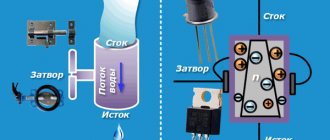
Before we start testing field-effect transistors, let’s consider what types of field-effect transistors there are.
In Figure 1 you see the classification of field-effect transistors.
From this figure it can be seen that field-effect transistors are divided into transistors with a control pn junction and field-effect transistors with an insulated gate.
In foreign literature, a field-effect transistor with a control pn junction is designated as JFET
(junction gate field-effect transistor), and an insulated gate transistor is
a MOSFET
(Metall-Oxid-Semiconductor FET).
Today I will tell you how to test a field-effect transistor with a control pn junction
, and in the next issue of the magazine we will move on to testing the MOSFET transistor, so don’t forget to subscribe to the magazine. Subscription form after the article.
First, let's briefly look at the structure of the transistor and the principle of its operation.
Field effect transistors are available in n-channel and p-channel types. In view of the fact that n-channel field-effect transistors have become widespread, using their example we will consider the operating principle of field-effect transistors with a control pn junction.
So, the transistor consists of an n-semiconductor with highly doped n-regions embedded in it with a high concentration of charge carriers - electrons. The semiconductor itself is located on a p-type substrate, which is connected to another p-type region. Together these areas are called the gate
(gate). Thus, each highly doped n-region creates its own pn junction with the p-substrate.
That part of the n-semiconductor that is located between the p-regions (gates) is called a channel (in particular, an n-type channel).
If a voltage source is connected to the highly doped n-regions, an electric field will be created in the channel; under the influence of this field, electrons from the n-region to which the “minus” of the source is connected will move to the n-region to which the “plus” of the voltage source is connected. Thus, an electric current will flow through the channel. The magnitude of this current will directly depend on the electrical conductivity of the channel, which in turn depends on the cross-sectional area of the channel. It is not difficult to guess that the cross-sectional area of the channel depends on the width of the pn junctions.
The region from which charge carriers move, and in the case of the n-channel these are electrons, is called the source
(source), and towards which they are moving -
drain
(drain).
If a negative voltage is applied to the gate relative to the source, then the pn junction formed between the gate and source will be biased in the opposite direction, while the width of the blocking layer will increase, thereby narrowing the size of the channel and reducing electrical conductivity.
Thus, by varying the voltage between gate and source, we can control the current through the FET channel.
That’s all about the design of a field-effect transistor; I won’t go into details further, since this will be enough to understand how to test a field-effect transistor with a control pn junction.
Based on the above, you can create an equivalent circuit of a field-effect transistor with a control pn junction, as we did when checking a bipolar transistor.
When drawing up a diagram, we will be guided by the following principles:
1. The transistor has two pn junctions, the first between the gate and the source, the second between the gate and the drain.
2. The channel between the source and drain, in the absence of a negative blocking voltage at the gate, is not closed and is electrically conductive, that is, it has a certain resistance value.
3. Now we will denote pn junctions by diodes, and the electrical conductivity of the channel by a resistor.
We make an equivalent circuit of a field-effect transistor with a control pn junction.
Now, knowing the equivalent circuit of a field-effect transistor with a control pn junction, you can build an algorithm or circuit for testing a field-effect transistor.
The history of transistors
At the dawn of the past centuries at the end of the 19th century, physicists and practitioners (Guthrie, Brown, Edison, Bowes, Picard, Fleming) from different countries made a fundamental discovery and received patents for a “detector”, “rectifier” - that’s what the diode was called then. The diode was followed by the epoch-making discovery of the transistor. Listing the names of scientists from different countries who put their head and hands to the discovery of the transistor would take many lines.
The main theorists are Shockley, who worked at Bell Telephone Laboratories, as well as his colleagues Bardeen and Brattain.
From left to right: Shockley, Bardeen and Brattain
As a result of their work, in 1947, the first sample of a working point-type germanium transistor was obtained, and on its basis, in the same year, the first amplifier was developed, which had a gain of 20 dB (10 times) at a frequency of 10 MHz.
Serial production of point-point transistors by Western Electric began in 1951 and reached about 10,000 units per month in 1952. In the USSR, the first point-point transistor was created in 1949. Serial production of point-point transistors was launched in 1952, and planar transistors in 1955. This was followed by the following discoveries in theory and technology: transistors based on grown junctions (1950), alloy transistors (1952), diffuse meta-transistors (1958), planar transistors (1960), epitaxial transistors (1963) .), multi-emitter transistors (1965), etc.
How did our hero, the Darlington transistor (hereinafter referred to as TD), appear among them? Darlington is a city in the UK. However, people can also have surnames based on cities or vice versa. This is an employee of the same Bell company - Sidney Darlington
Sydney Darlington
Why was this “sweet couple” needed? The fact is that the first transistors had very mediocre characteristics, if you look at today's successes. First of all, the gain is low. Now this seems strange - just think, a cascade connection is elementary! But then, in 1953, this was pioneering work.
Electronics for everyone
Except transistors
Darlington
assemblies, there is another good way to drive a powerful constant load -
MOSFETs . A field-effect transistor operates like a conventional transistor - a weak signal at the gate controls a powerful flow through the channel. But, unlike bipolar transistors, here the control is not by current, but by voltage .
MOS (in bourgeois MOSFET ) stands for Metal-Oxide-Semiconductor; from this abbreviation the structure of this transistor becomes clear.
If on the fingers, then it has a semiconductor channel that serves as one plate of the capacitor and the second plate is a metal electrode located through a thin layer of silicon oxide, which is a dielectric. When voltage is applied to the gate, this capacitor is charged, and the electric field of the gate pulls charges to the channel, as a result of which mobile charges appear in the channel that can form an electric current and the drain-source resistance drops sharply. The higher the voltage, the more charges and lower the resistance, as a result, the resistance can drop to tiny values - hundredths of an ohm, and if you raise the voltage further, a breakdown of the oxide layer and the Khan transistor will occur. The advantage of such a transistor, compared to a bipolar one, is obvious - voltage must be applied to the gate, but since there is a dielectric, the current will be zero, which means the required power to control this transistor will be negligible; in fact, it consumes only at the moment of switching, when charging is in progress and capacitor discharge.
The disadvantage arises from its capacitive property - the presence of capacitance on the gate requires a large charging current when opening. In theory, equal to infinity on infinitely small periods of time. And if the current is limited by a resistor, then the capacitor will charge slowly - there is no escape from the time constant of the RC circuit.
MOS transistors come in P and N channel. They have the same principle, the only difference is the polarity of the current carriers in the channel. Accordingly, in different directions of the control voltage and inclusion in the circuit. Very often transistors are made in the form of complementary pairs. That is, there are two models with exactly the same characteristics, but one of them is N channel, and the other is P channel. Their markings, as a rule, differ by one digit.
The load is connected to the drain circuit. In general, in theory, it makes no difference to a field-effect transistor what is considered a source and what is a drain - there is no difference between them. But in practice there is, the fact is that to improve the characteristics, the source and drain are made of different sizes and designs, plus, in powerful field devices there is often a reverse diode (it is also called parasitic, because it is formed by itself due to the peculiarities of the technical process production).
My most popular MOS transistors are IRF630 (n channel) and IRF9630 (p channel). At one time I installed about a dozen of each type. Possessing a not very large TO-92 , this transistor can easily pull through itself up to 9A. Its open resistance is only 0.35 Ohm. However, this is a rather old transistor; now there are better things, for example IRF7314 , capable of carrying the same 9A, but at the same time it fits into an SO8 case - the size of a notebook square.
One of the problems of joining MOSFET transistor and a microcontroller (or digital circuit) is that in order to fully open until completely saturated, this transistor needs to drive quite a higher voltage to the gate. Usually this is about 10 volts, and the MK can output a maximum of 5. There are three options:
- Using smaller transistors, build a chain that supplies power from the high-voltage circuit to the gate in order to pump it with high voltage
- use a special driver chip, which itself will generate the required control signal and equalize the levels between the controller and the transistor. Typical examples of drivers are, for example, IR2117.
You just need to remember that there are upper and lower shoulder drivers (or combined, half-bridge). The choice of driver depends on the load connection circuit and the switching transistor. If you pay attention, you will see that N channel transistors are used with the driver in both the upper and lower arms. They just have better characteristics than P channel ones. But here another problem arises. In order to open the N channel transistor in the upper side, it needs to apply a voltage higher than the drain voltage to its gate, and this, in fact, is higher than the supply voltage. To achieve this, a voltage pump is used in the high-side driver. What exactly is the difference between a lower shoulder driver and an upper shoulder driver?
- Use a transistor with a low turn-on voltage. For example, from the IRL630A series or the like. Their opening voltages are tied to logical levels. They do have one drawback - they are sometimes difficult to get. If ordinary powerful field workers are no longer a problem, then those controlled by the logical level are not always the case.
But in general, it is more correct to install a driver, because in addition to the main functions of generating control signals, it also provides current protection, protection against breakdown, overvoltage, as an additional bauble, optimizes the opening speed to the maximum, in general, it does not consume its current in vain.
Choosing a transistor is also not very difficult, especially if you don’t bother with limiting modes. First of all, you should be concerned about the value of the drain current - I Drain or ID; you select a transistor based on the maximum current for your load, preferably with a margin of 10 percent. The next important parameter for you is VGS - Source-Gate saturation voltage or, more simply put, control voltage. Sometimes it is written, but more often you have to look at the charts. You are looking for a graph of the output characteristics Dependence of ID on VDS at different values of VGS . And you figure out what kind of regime you will have.
For example, you need to power the engine at 12 volts, with a current of 8A. You screwed up the driver and only have a 5 volt control signal. The first thing that came to mind after this article was IRF630. The current is suitable with a margin of 9A versus the required 8. But let’s look at the output characteristic:
You see, at 5 volts on the gate and a current of 8A, the voltage drop across the transistor will be about 4.5V. According to Ohm's law, then it turns out that the resistance of this transistor at the moment is 4.5/8 = 0.56 Ohm . Now let’s calculate the power losses - your engine consumes 5A. P=I*U or, if we apply the same Ohm's law, P=I2R . At 8 amperes and 0.56 Ohm the loss will be 35 W. It hurts a lot, don't you think? I also think it’s too much. the IRL630 then .
At 8 amps and 5 volts on the Gate, the voltage across the transistor will be about 3 volts. Which will give us 0.37 Ohm and 23 W losses, which is noticeably less.
If you are going to use PWM on this switch, then you need to inquire about the opening and closing times of the transistor, choose the largest one and, relative to the time, calculate the maximum frequency of which it is capable. This value is called Switch Delay or ton , toff , in general, something like that. Well, the frequency is 1/t. It would also be a good idea to look at the gate capacitance Ciss , based on it, as well as the limiting resistor in the gate circuit, you can calculate the charging time constant of the RC gate circuit and estimate the performance. If the time constant is greater than the PWM period, then the transistor will not open/close, but will hang in some intermediate state, since the voltage at its gate will be integrated by this RC circuit into a constant voltage.
When handling these transistors, take into account the fact that they are not just very afraid of static electricity, but VERY STRONG . It is more than possible to penetrate the shutter with a static charge. So when you buy it, immediately wrap it in foil and don’t take it out until you seal it. First ground yourself to the battery and put on a foil hat :).
And in the process of designing a circuit, remember one more simple rule - under no circumstances should you leave the field gate shutter hanging just like that - otherwise it will eat noise from the air and open on its own. Therefore, it is necessary to install a 10 kilo-ohm resistor from Gate to GND for N channel or +V for P channel, so that the parasitic charge flows off. That seems to be all, next time I’ll write about bridge circuits for controlling engines.
What is an NPN transistor?
Transistors replaced electric lamps and made it possible to reduce the number of relays and switches in devices. These are semiconductor triodes - radio-electronic components made from semiconductors; they have 3 terminals as standard.
Transistors are designed to control current, that is, the main power factor of electrical circuits; it is its shock (not voltage) that poses a danger to humans.
The element is capable of controlling extremely high values in output circuits when applying a weak input signal. Transistors boost, generate, switch, and convert electrical signals; they are the basis of microelectronics and electrical devices.
Varieties based on operating principle:
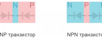
- bipolar transistor made of 2 types of conductors, the basis of its operation is the interaction of adjacent pn sections on the crystal. They consist of an emitter/collector/base (hereinafter, we will abbreviate these terms): the latter receives a weak current, causing a modification of the resistance (hereinafter referred to as “resistance”) in the line consisting of the first 2 elements. Thus, the flowing quantity changes, the side of its unidirectionality (npn or pnp) is determined by the characteristics of the transitions (sections) in accordance with the polarity of the connection (reverse, forward). Control is carried out by modulating the current on the base/emitter segment, the output of the latter is always common for control and output signals;
- field. There is only one type of conductor - a narrow channel subject to the electric field of a separate gate passage. Control is based on modulating the number of volts between it and the source. And between the latter and the drain an electric current flows (2 working contacts). The value has a strength depending on the signals generated between the gate (control contact) and one of the specified parts. There are products with a pn control section (working contacts are connected to a p- or n-semiconductor) or with separate gates.
Field workers have polarity options; low voltage is required for control; due to their efficiency, they are installed in radio circuits with low-power power supplies. Bipolar variants are activated by currents. In analog assemblies, the latter (BT, BJT) prevail, in digital (processors, computers) - the former. There are also hybrids - IGBTs, used in power circuits.
Checking a field-effect transistor with a control pn junction and a p-type channel.
Testing a field-effect transistor with a control pn junction and a p-type channel is carried out according to the above algorithm, except that when checking pn junctions, the polarity of connecting the multimeter probes is reversed.
For clarity and ease of understanding of the process, I recorded a video for you on how to check a field-effect transistor with a control pn junction, where I check a transistor with a p-type channel.
In technology and amateur radio practice, field-effect transistors are often used. Such devices differ from conventional bipolar transistors in that in them the output signal is controlled by a control electric field. Insulated gate field effect transistors are especially often used.
The English designation for such transistors is MOSFET, which means “field-controlled metal-oxide semiconductor transistor.” In the domestic literature, these devices are often called MOS or MOS transistors. Depending on the manufacturing technology, such transistors can be n- or p-channel.
An n-channel type transistor consists of a silicon substrate with p-conductivity, n-regions obtained by adding impurities to the substrate, and a dielectric that insulates the gate from the channel located between the n-regions. The pins (source and drain) are connected to the n-regions. Under the influence of a power source, current can flow from source to drain through the transistor. The magnitude of this current is controlled by the insulated gate of the device.
When working with field-effect transistors, it is necessary to take into account their sensitivity to the effects of an electric field. Therefore, they must be stored with the terminals short-circuited with foil, and before soldering, the terminals must be short-circuited with a wire. Field-effect transistors must be soldered using a soldering station, which provides protection against static electricity.
Before you start checking the serviceability of the field-effect transistor, you need to determine its pinout. Often, on an imported device, marks are applied that identify the corresponding terminals of the transistor.
The letter G denotes the gate of the device, the letter S the source, and the letter D the drain.
If there is no pinout on the device, you must look it up in the documentation for this device.
NPN transistor design
The transistor design of an NPN transistor consists of two regions of p-type semiconductor material on either side of a region of n-type material, as shown in the figure below.
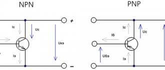
The arrow identifies the emitter and the generally accepted direction of its current (“inward” for a PNP transistor).
The PNP transistor has very similar characteristics to its NPN bipolar counterpart, except that the directions of currents and voltage polarities in it are reversed for any of the possible three connection schemes: common base, common emitter and common collector.
Video on how to test a field-effect transistor
Semiconductor elements are used in almost all electronic circuits. Those who call them the most important and most common radio components are absolutely right. But any components do not last forever; overvoltage and current, temperature violations and other factors can damage them. We will tell you (without overloading with theory) how to check the performance of various types of transistors (npn, pnp, polar and composite) using a tester or multimeter.
Before checking any element with a multimeter for serviceability, be it a transistor, thyristor, capacitor or resistor, it is necessary to determine its type and characteristics. This can be done by marking. Once you know it, it won’t be difficult to find a technical description (datasheet) on thematic sites. With its help, we will find out the type, pinout, main characteristics and other useful information, including replacement analogues.
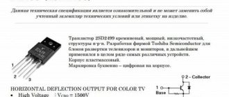
For example, the scanning on the TV stopped working. Suspicion is raised by the line transistor marked D2499 (by the way, a fairly common case). Having found a specification on the Internet (a fragment of it is shown in Figure 2), we receive all the information necessary for testing.
Figure 2. Specification fragment for 2SD2499
There is a high probability that the datasheet found will be in English, no problem, the technical text is easy to understand even without knowledge of the language.
Having determined the type and pinout, we solder the part and begin testing. Below are the instructions with which we will test the most common semiconductor elements.
NPN transistor circuit
When an NPN transistor is connected to voltage resources, base current will flow through the transistor. Even a small amount of base controls the circulation of a large amount of current through the emitter to the collector. The base voltage is higher than the emitter voltage.
It will be interesting➡ Protective grounding. Main and additional potential equalization systems. Third party conductive parts. Grounding in a private house
When VB base voltage is not -ve compared to VE emitter voltage, current cannot flow in the circuit. Therefore, it is necessary to provide a reverse bias voltage of >0.72 Volts.
Resistors RL and RB are included in the circuit. This limits the current passing through the maximum possible height of the transistor.
Emitter voltage VEB as input side. Here, the emitter current (IE) flows from the input side and flows in two directions; one is IB and the other is IC.
IE= YaB+ YaC
The main differences between the two types of bipolar transistors
The main difference between them is that holes are the main current carriers for PNP transistors, NPN transistors have electrons in this capacity. Therefore, the polarities of the voltages supplying the transistor are reversed, and its input current flows from the base. In contrast, with an NPN transistor, the base current flows into it, as shown below in the circuit diagram for connecting both types of devices with a common base and a common emitter.
The operating principle of a PNP-type transistor is based on the use of a small (like the NPN-type) base current and a negative (unlike the NPN-type) base bias voltage to control a much larger emitter-collector current. In other words, for a PNP transistor, the emitter is more positive with respect to the base and also with respect to the collector.
Indeed, it can be seen that the collector current IC (in the case of an NPN transistor) flows from the positive terminal of battery B2, passes through the collector terminal, penetrates into it and must then exit through the base terminal to return to the negative terminal of the battery. In the same way, looking at the emitter circuit, you can see how its current from the positive terminal of battery B1 enters the transistor through the base terminal and then penetrates into the emitter.
The base terminal thus carries both the collector current IC and the emitter current IE. Since they circulate in opposite directions along their circuits, the resulting base current is equal to their difference and is very small, since IC is slightly smaller than IE. But since the latter is still larger, the direction of flow of the difference current (base current) coincides with IE, and therefore a PNP-type bipolar transistor has a current flowing out of the base, and an NPN-type one has an inflowing current.
Driver chip selection criteria
Let's look at an example of choosing a driver for the CoolSiC IMW120R045M1 transistor manufactured by Infineon. Table 2 shows the information from the transistor specification necessary to select a driver.
Table 2. Fragment of the specification of the transistor IMW120R045M1
| Limit values | |||
| Parameter | Symbol | Magnitude | |
| Drain-source voltage, V | VDSS | 1200 | |
| The drain current for Rth(jc,max) is limited to Tvjmax, VGS = 15 V, A | TC = 25°C | ID | 52 |
| TC = 100°C | 36 | ||
| Gate-Source Voltage | VGSS | -10/+20* | |
| * – A bipolar gate driver can be used. | |||
The choice of positive and negative gate voltages affects the life of the device. To ensure the required service life, the recommendations described in AN 2018-19 should be taken into account.
To select a negative gate voltage, we will use the graph (Figure 13) from AN 2018-19 for a positive gate voltage VCC2 = 15 V, although the IMW120R045M1 transistor can operate at a voltage VCC2 = 18 V.
Rice. 13. Selection of negative gate voltage according to AN 2018-19
The normalized switching frequency depends on the service life of the device and is calculated using formula 8:
$$Nf_{SW}=\frac{Af_{SW}\times T_{S}\times OT}{10},\qquad{\mathrm{(}}{8}{\mathrm{)}}$$
Where:
- NfSW – normalized switching frequency, kHz;
- AfSW – actual switching frequency, kHz;
- Ts – device service life, years
- OT – percentage of working time of the total, %
Thus, the greater the negative voltage, the shorter the normalized frequency and, accordingly, the service life of the device.
According to Figure 13, for a normalized frequency of 100 kHz, a negative voltage VEE2 = -2.8 V is obtained. However, lower voltages can be used. The minimum voltage VEE2 must be such that the RDS(on) resistance increases by no more than 15% at rated current and Tj = 125°C. In this example, to provide some safety margin, we will take VEE2 = -2 V.
External resistor RG,ext is calculated based on formula 9:
$$R_{G,ext}=\frac{V_{Drive}\times (t_{r}+t_{d(on)})}{Q_{Gate}},\qquad{\mathrm{(}}{ 9}{\mathrm{)}}$$
Where:
QGate is defined according to Figure 4;
- tr = 24‧10-9 s and td(on) = 9‧10-9 s (values are taken from the specification for the IMW120R045M1 transistor;
- VDrive = VCC2 – VEE2 = 17 V;
- QGate, according to Figure 4, is taken to be approximately 60‧10-9 C.
Thus we get RG,ext = 9.35 Ohm ≈ 10 Ohm.
Let's calculate the maximum gate current using formula 10 with RG,int = 4 Ohm, RG,ext = 10 Ohm, RDS(on) = 0 Ohm:
$$R_{G\_Total}=R_{DS(on)}+R_{G,ext}+R_{G,int};\\V_{Drive}=VCC2-VEE2;\:I_{Gmax}=\ frac{V_{Drive}}{R_{G\_Total}}\qquad{\mathrm{(}}{10}{\mathrm{)}}$$
Since the calculation is carried out for the first time and the value of RDS(on) is unknown, it is equal to zero.
We get IGmax ≈ 1.21 A.
Let's calculate the maximum power dissipation in the driver control circuit using formula 11:
$$P_{vtot}=Q_{G}\times dV_{Drive}\times f_{SW},\qquad{\mathrm{(}}{11}{\mathrm{)}}$$
Pvtot = 0.102 W.
It is important to fulfill the following conditions:
Pvtot ≤ PDOUT,
where PDOUT is the maximum output power of the driver according to the specification.
Based on the calculations, we select the appropriate driver produced by Infineon from Table 3.
Table 3. Recommended list of drivers for SiC MOSFETs
| Name, body | Typical peak control current, A | VCC2-VEE2, V | Typical propagation delay, ns | Active suppression of the Miller effect | Short circuit protection |
| 1EDI20I12MF | 3,5 | 20 | ≤300 | + | – |
| DSO-8 150mil | |||||
| 1EDC20H12AH | 3,5 | 40 | ≤125 | – | – |
| DSO-8 300mil | |||||
| 1EDC60H12AH | 9,4 | 40 | ≤125 | – | – |
| DSO-8 300mil | |||||
| 1EDC20I12MH | 3,5 | 20 | ≤300 | + | – |
| DSO-8 300mil | |||||
| 1ED020I12-F2 | 2 | 28 | ≤170 | + | + |
| DSO-16 300mil | |||||
| 2ED020I12-F2 | 2 | 28 | ≤170 | + | + |
| DSO-36 |
The most suitable driver for the example discussed in this section is the 1ED020I12-F2 chip.
How does an NPN transistor work?
When you and I, my friends, have figured out what this transistor is, let's find out how it works. It is designed quite simply, you just need to understand the principle. To do this, we introduce two very important concepts: emitter and collector. The emitter (as in the word emission) releases charges and they move towards the collector. So, in a state of rest, when, roughly speaking, everything is turned off, no current flows in the transistor, because there is a semiconductor junction between the emitter and the collector. However, when a small voltage is applied to the base of the transistor, the current begins to flow and it can even be amplified. How? Oscillations of a small current are exactly repeated, but with a larger amplitude. Here is a circuit diagram of a simple transistor:
In this new circuit, the base-emitter PN junction is biased by battery voltage B1 and the collector-base junction is reverse biased by battery voltage B2. The emitter terminal is thus common to the base and collector circuits.
The total emitter current is given by the sum of the two currents IC and IB; passing through the emitter terminal in one direction. Thus we have IE = IC + IB.
In this circuit, the base current IB simply “branches” from the emitter current IE, also coinciding with it in direction. In this case, a PNP-type transistor still has current IB flowing out of the base, and an NPN-type transistor has flowing current.
NPT devices
Unlike PT IGBTs, NPT transistors, such as the 4th generation from IR, have a p+ doped region on the bottom side of the n-type substrate. Since this zone is relatively thin, processing the substrate is cheaper. There is no n+ buffer layer. Despite the superficial similarity, the difference between these two device structures is significant. The on and off states are implemented in a similar way, but in NPT transistors there is no clamping effect, which reduces the charge accumulation time and encourages carriers to recombine in the base-emitter junction of the native PNP structure. As a result, the “tail” of the collector current when turning off NPT transistors is slightly longer than that of PT devices, and other characteristics are identical.
Due to the lower current gain of the native pnp structure, the VCE(SAT) voltage of the PT transistors is slightly higher than that of the NPT, making it easier to control the maximum current of the lower gain pnp transistor using the native n-channel MOSFET. This means that the short circuit duration of the NPT device is well defined and controlled. The value of this parameter for NPT IGBT is in the range of up to 10 μs.
Finally, the characteristics of n-channel MOSFET are superior to NPT IGBT. This means that the voltage VCE(SAT) increases with temperature, allowing these devices to be connected in parallel to each other.
Checking bipolar types
Below is a diagram for checking npn, pnp transistors with a tester, after which we will describe the procedure point by point.
The bipolar transistor is equipped with pn lines - conventionally, these are diodes, or rather, 2 of them located oppositely, the point of their intersection is the “base”.
One conditional diode is designed with base/collector contacts, the other with base/emitter contacts. For analysis, just look at the contrast. (directly and back) of the indicated areas: if there are no problems there, then the part is without flaws.
Do-it-yourself testing without soldering a bipolar pnp, npn transistor involves testing 3 combinations of legs:
pnp option
Structures (types) are shown by the arrow emitting. section: pnp/npn (to/from the base). Let's start by checking the first option. We open the PNP part by applying negative voltage to the base. On the multimeter, we set the selector to measure Ohms to o; it is also possible to set it to “continuity”.
The vein “−” (black) is on the base leg. Plus (red) - alternately to collect., emitter. If the areas are not damaged, they will display about 500–1200 Ohms.
Next we will describe how to ring the reverse resistance: “+” - to the base, “−” - to the call. and emits. High resistance should be displayed. on both pn sites. We now have “1”, that is, for the frame set to “2000” the value exceeds 2000. This means that there are 2 transitions without breaks, the product is in good working order.
It will be interesting➡ Reactance
Similarly, as described, you can test the transistor for serviceability without removing it from the circuit. Less commonly, there are assemblies where substantial shunting is applied to the transitions, for example, with resistors. Then, if too low resistance is displayed, the part will need to be desoldered.
npn structure
Npn elements are checked in the same way, only the “+” probe goes to the base from the tester.
Symptoms of a problem
If the resistance (direct and reverse) of one of the sections (pn) tends to infinity, that is, at o and above on the display “1”, which means that this section has a break, the transistor is unusable. If “0” means the product is also flawed, the area is broken. Direct cont. there should be 500–1200 ohms.
A slight digression from the topic
A completely reasonable question arises. If new products have better parameters and are cheaper, then what is the point of those products with which we compared them? What is their niche?
Note that these products were developed five or more years ago and their characteristics corresponded to that time. In addition, IR has a policy of focusing its efforts on those areas where it has advantages over other manufacturers of power electronics components. It was the massive introduction of TrenchFET technology in new products that made it possible to dramatically improve technical characteristics and reduce costs.
For the niche of previously developed transistors, it is necessary to determine whether this is a new development or a direct replacement for the Benchmark MOSFET in consumer mass-produced products.
There is probably no reason to use previously released transistors in new designs, except for some very specific products and very specific parameters.
As for direct replacement, for a serious end manufacturer this involves, at a minimum, adjusting the design documentation. If the position being replaced in the product is not price determining, then the game may not be worth the candle. For critical applications (military equipment and not only), such a replacement may entail repeated tests confirming compliance with the requirements of the technical specifications, or confirmation of tactical and technical characteristics. And these are costs, and serious ones. Actually, this is the answer to the question about the niche of “early” products.
Conclusion: the feasibility of using “reference” products in new developments is beyond doubt. The possibility of using their direct replacement is not in doubt from a technical point of view, but requires thoughtful analysis from a financial point of view.
Checking a simple transistor circuit
Assemble a circuit with a transistor as shown in the figure. In this circuit, the transistor acts as a “key”. Such a circuit can be quickly assembled on a printed circuit board, for example. Pay attention to the 10Kohm resistor, which is included in the base of the transistor.
This is very important, otherwise the transistor will “burn out” during the test. If the transistor is working properly, then when you press the button the LED should light up and when released, it should go out. This circuit is for testing NPN transistors. If you need to check the PNP transistor, in this circuit you need to swap the LED contacts and connect the power supply the other way around. Testing a transistor with a multimeter is simpler and more convenient. In addition, there are multimeters with a function for checking transistors. They show the base current, collector current and even the gain of the transistor.
Circuit for checking an n-channel field-effect transistor with a multimeter
Before checking the serviceability of the field-effect transistor, it is necessary to take into account that in modern MOSFET-type radio components there is an additional diode between the drain and the source. This element is usually present on the device diagram. Its polarity depends on the type of transistor.
The general rules are to begin the procedure by determining the performance of the measuring device itself. Having made sure that it works flawlessly, they move on to further measurements.
Conclusions:
- MOSFET field-effect transistors are widely used in technology and amateur radio practice.
- The performance of such transistors can be checked using a multimeter, following a certain method.
- Testing a p-channel field-effect transistor with a multimeter is carried out in the same way as an n-channel transistor, except that the polarity of the multimeter leads should be reversed.
Step-by-step instructions for checking with a multimeter
Before starting the test, first of all, the structure of the triode device is determined, which is indicated by the emitter junction arrow. When the direction of the arrow points towards the base, then this is the PNP variant, the direction opposite to the base indicates NPN conductivity.
Testing an NPN transistor with a multimeter consists of the following sequential operations:
- We check the reverse resistance; to do this, we connect the “positive” probe of the device to its base.
- The emitter junction is tested; for this we connect the “negative” probe to the emitter.
- To check the collector, move the negative probe onto it.
The results of these measurements should show a resistance within the value of “1”.
To check direct resistance, swap the probes:
- We attach the “negative” probe of the device to the base.
- We alternately move the “positive” probe from the emitter to the collector.
- On the multimeter screen, the resistance readings should be from 500 to 1200 Ohms.
These readings indicate that the transitions are not broken, the transistor is technically sound.
Many amateurs have difficulty identifying the base, and, accordingly, the collector or emitter. Some advise starting to determine the base, regardless of the type of structure, in this way: alternately connecting the black probe of the multimeter to the first electrode, and the red probe alternately to the second and third.
The base will be detected when the voltage across the device begins to drop. This means that one of the transistor pairs has been found - “base-emitter” or “base-collector”. Next, you need to determine the location of the second pair in the same way. The common electrode of these pairs will be the base.
Literature
1. V. Bashkirov, New families of high-efficiency low-voltage MOSFETs, Electronics News, No. 18, 2008
2. Shevchenko V. Transistors in DirectFET packages from International Rectifier // Chip News Ukraine, 2006, No. 1.
3. Benchmark MOFSETs. Product Selection Guide // material from International Rectifier.
Obtaining technical information, ordering samples, delivery - e-mail
•••
Main causes of malfunction
The most common reasons for a triode element in an electronic circuit to fail to operate are as follows:
- Break in the transition between components.
- Breakdown of one of the transitions.
- Breakdown of the collector or emitter section.
- Power leakage under voltage.
- Visible damage to the terminals.
Characteristic external signs of such a breakdown are blackening of the part, swelling, and the appearance of a black spot. Since these shell changes occur only with high-power transistors, the issue of diagnosing low-power ones remains relevant.
Adviсe
- There are many ways to determine a malfunction, but first you need to understand the structure of the element itself and clearly understand the design features.
- The choice of device for testing is an important point regarding the quality of the result. Therefore, if you lack experience, you should not limit yourself to improvised means.
- When carrying out the test, you should clearly understand the reasons for the failure of the tested part, so as not to return over time to the same state of failure of household electrical appliances.
How does a transistor switch work?
In this article we will look at how a transistor switch on a bipolar transistor works. Such semiconductor elements are produced in two types - npn and pnp structures, which differ in the type of semiconductor used (in a p-semiconductor, positive charges - “holes" - predominate; in an n-semiconductor, negative charges - electrons).
The BT terminals are called base, collector and emitter, which have a graphical designation on electrical circuit drawings, as shown in the figure.
In order to understand the operating principle and individual processes occurring in bipolar transistors, they are depicted as two diodes connected in series and back-to-back.
The most common diagram of a BT operating in key mode is shown below.
To open a transistor switch, you need to apply potentials of a certain sign to both pn junctions. The collector-base junction must be reverse biased, and the base-emitter junction must be forward biased. To do this, the electrodes of the power supply UKE are connected to the terminals of the base and collector through a load resistor RK. Please note that the positive potential UKE is supplied to the collector via RK, and the negative potential is supplied to the emitter. For a semiconductor pnp structure, the polarity of connecting the power supply UKE is reversed.
It might be interesting➡ DC power supply
The resistor in the collector circuit RK serves as a load, which simultaneously protects the bipolar transistor from short circuit.
The command to open the BT is supplied by the control voltage UBE, which is supplied to the base and emitter terminals through the current-limiting resistor RB. The value of UBE must be at least 0.6 V, otherwise the emitter junction will not open completely, which will cause additional energy losses in the semiconductor element.
In order not to confuse the polarity of connecting the supply voltage UKE and the control signal UBE BT of different semiconductor structures, pay attention to the direction of the emitter arrow. The arrow points in the direction of the flow of electric current. Focusing on the direction of the arrow, it is enough to simply position the voltage sources in the correct way.
The use of a transistor switch in conjunction with an MK
A transistor switch can very often be seen in circuits where an MK or other logical element switches a powerful load. As you remember, the maximum current that an MK can produce per leg is 20 milliamps. Therefore, most often you can see this circuit design on a bipolar transistor in switch mode:
There is no need for an RBE resistor, because the outputs of the MK are “pulled up” to zero even during programming.
Conditions for operation of a transistor switch
So, let's remember what requirements must be in order to completely “open” the transistor? We read the article on the principle of amplification of a bipolar transistor and remember:
1) In order to fully open the transistor, the base-emitter voltage must be greater than 0.6-0.7 Volts.
2) The current flowing through the base must be such that the electric current can flow through the collector-emitter absolutely unimpeded. Ideally, the resistance through the collector-emitter should be zero, but in reality it will be fractions of an Ohm. This mode is called “saturation mode”.
This drawing is the imagination of my mind. Here I drew the same saturation mode.
As we can see, the collector and emitter are short-circuited in saturation mode, so the light bulb burns at full power.
Checking the functionality of the field-effect transistor
This type of semiconductor elements is also called mosfet and mosfet components. Figure 4 shows the graphic designation of n- and p-channel field switches in circuit diagrams.
Figure 4. Field-effect transistors (N- and P-channel)
To test these devices, we connect the probes to the multimeter in the same way as when testing bipolar semiconductors, and set the test type to “continuity”. Next, we proceed according to the following algorithm (for an n-channel element):
- We touch the black wire to the “c” pin, and the red wire to the “i” pin. The resistance on the built-in diode will be displayed, remember the reading.
- Now you need to “open” the transition (this will only be possible partially), for this we connect the probe with the red wire to terminal “z”.
- We repeat the measurement carried out in step 1, the reading will change downwards, which indicates a partial “opening” of the field worker.
- Now you need to “close” the component, for this purpose we connect the negative probe (black wire) to the “z” leg.
- We repeat steps 1, the original value will be displayed, therefore, “closing” has occurred, which indicates the serviceability of the component.
To test p-channel elements, the sequence of actions remains the same, with the exception of the polarity of the probes, it must be reversed.
Note that insulated gate bipolar elements (IGBT) are tested in the same way as described above. Figure 5 shows the SC12850 component in this class.
Fig 5. IGBT transistor SC12850
For testing, it is necessary to perform the same steps as for a field-effect semiconductor element, taking into account that the drain and source of the latter will correspond to the collector and emitter.
In some cases, the potential on the multimeter probes may not be enough (for example, to “open” a powerful power transistor); in such a situation, additional power will be needed (12 volts will be enough). It must be connected through a resistance of 1500-2000 Ohms.
Practice of compound transistor operation
In Fig. Figure 3 shows three options for constructing an output stage (emitter follower). When selecting transistors, you should strive for b1~b2 and b3~b4. The difference can be compensated by selecting pairs based on the equality of the ST gain factors b13~b24 (see Table 1).
- Scheme in Fig. 3a has the highest input resistance, but this is the worst of the given circuits: it requires insulation of the flanges of powerful transistors (or separate radiators) and provides the smallest voltage swing, since ~2 V must drop between the bases of the CT, otherwise “step” distortion will appear strongly.
- Scheme in Fig. 3b was inherited from those times when complementary pairs of powerful transistors were not yet produced. The only advantage compared to the previous version is a lower voltage drop of ~1.8 V and a larger swing without distortion.
- Scheme in Fig. 3c clearly demonstrates the advantages of STS: a minimum voltage drops between the ST bases, and powerful transistors can be placed on a common radiator without insulating spacers.
In Fig. Figure 4 shows two parametric stabilizers. The output voltage for the version with STD is:
Since Ube varies depending on temperature and collector current, the output voltage spread of a circuit with STD will be greater, and therefore the option with STS is preferable.
Rice. 3. Options for output emitter followers on ST
Rice. 4. Application of CT as a regulator in a linear stabilizer
Any suitable combination of transistors can be used in linear circuits. The author has encountered Soviet household appliances that used STS in pairs KT315+KT814 and KT3107+KT815 (although /KT361 and KT3102/KT3107 are accepted). As a complementary pair, you can take C945 and A733, often found in old computer power supplies.
For switching electromechanical drives and, especially, in pulse circuits, ready-made CTs with standardized on and off parameters and parasitic capacitances should be used. A typical example is the widespread imported complementary STD of the TIP12x series.
New “reference” 150- and 200-volt MOSFETs
Also in August 2009, International Rectifier announced new 150- and 200-volt MOSFETs: IRx4615 and IRx4620, respectively. The transistors are available in D2-Pak surface mount packages (prefix IRFS) and through-hole solder packages TO-220AB and TO-262 (prefixes IRFB and IRFSB, respectively). They switch currents up to 35 and 25 A, are characterized by extremely low gate charge and are intended for industrial applications such as switching power supplies, uninterruptible power supplies, inverters, and DC motor drives.
In addition, International Rectifier has released transistors IRx5615 and IRx5620, the main parameters of which are similar to IRx4615 and IRx4620. The IRx56xx transistors are specifically designed for digital audio applications, particularly Class D audio amplifiers. Their parameters are optimized to increase amplifier efficiency, reduce electromagnetic interference and non-linear distortion.
Let's look at the lines of 150- and 200-volt IR transistors (the technical characteristics of which are given in Table 2) and compare the parameters of new and previously released devices.
Table 2. Line of 150- and 200-volt MOSFET transistors (TO-220AB package)
| Model | VBRD, max, V | VGS, max, V | RDS(ON), max, mOhm | ID, A | QG, typ, nK | RxQ, mOhm x nK |
| IRL3215 | 150 | 16 | 166 | 12 | 21 | 3436 |
| IRFB4019 | 150 | 20 | 95 | 17 | 13 | 1235 |
| IRF3315 | 150 | 20 | 70 | 21 | 63 | 4431 |
| IRFB23N15D | 150 | 30 | 90 | 23 | 37 | 3330 |
| IRFB33N15D | 150 | 30 | 56 | 33 | 60 | 3360 |
| IRFB4615 | 150 | 20 | 39 | 35 | 26 | 1014 |
| IRFB5615 | 150 | 20 | 39 | 35 | 26 | 1014 |
| IRFB41N15D | 150 | 30 | 45 | 41 | 72 | 3240 |
| IRF3415 | 150 | 20 | 42 | 43 | 133 | 5599 |
| IRFB52N15D | 150 | 30 | 32 | 60 | 60 | 1920 |
| IRFB61N15D | 150 | 30 | 32 | 60 | 95 | 3040 |
| IRFB4321 | 150 | 30 | 15 | 83 | 71 | 1065 |
| IRFB4115 | 150 | 20 | 11 | 104 | 77 | 847 |
| IRF630N | 200 | 20 | 300 | 9 | 23 | 6990 |
| IRFB17N20D | 200 | 30 | 170 | 16 | 33 | 5610 |
| IRFB4103 | 200 | 30 | 165 | 17 | 25 | 4125 |
| IRFB4020 | 200 | 20 | 100 | 18 | 18 | 1800 |
| IRF640N | 200 | 20 | 150 | 18 | 45 | 6705 |
| IRFB23N20D | 200 | 30 | 100 | 24 | 57 | 5700 |
| IRFB4620 | 200 | 20 | 73 | 25 | 25 | 1813 |
| IRFB5620 | 200 | 20 | 73 | 25 | 25 | 1813 |
| IRFB31N20D | 200 | 30 | 82 | 31 | 70 | 5740 |
| IRFB42N20D | 200 | 30 | 55 | 43 | 91 | 5005 |
| IRFB38N20D | 200 | 30 | 54 | 44 | 60 | 3240 |
| IRFB260N | 200 | 20 | 40 | 56 | 150 | 6000 |
| IRFB4227 | 200 | 30 | 26 | 65 | 70 | 1820 |
| IRFB4127 | 200 | 20 | 20 | 76 | 100 | 2000 |
An analysis of the table shows that the new devices IRFB4615 and IRFB5615 can be offered as a replacement for products such as the IRFB33N15D and IRFB41N15D, and the IRFB4620 and IRFB5620 can be offered as a replacement for the IRFB23N20D transistor. However, we note that the maximum permissible value of the control voltage VGS for new devices is 20 V (instead of 30 V for previously produced ones). Therefore, an analysis of the electrical circuit still needs to be carried out. Conclusion: the comprehensive loss indicator has been reduced by three or more times. The price of IRFB46xx is slightly, but lower than that of previous products. For IRFB56xx the savings are 30...40%.