It is perhaps difficult today to imagine the modern world without transistors; in almost any electronics, from radios and televisions, to cars, telephones and computers, they are used in one way or another.
There are two types of transistors: bipolar and field-effect . Bipolar transistors are controlled by current, not voltage. There are high-power and low-power, high-frequency and low-frequency, pnp and npn structures. Transistors come in different packages and sizes, ranging from SMD chips (actually much smaller than a chip) that are designed for surface mounting, to very high power transistors. Based on power dissipation, there are low-power transistors up to 100 mW, medium-power transistors from 0.1 to 1 W, and high-power transistors greater than 1 W.
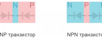
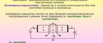
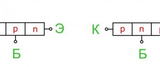
When people talk about transistors, they usually mean bipolar transistors. Bipolar transistors are made of silicon or germanium. They are called bipolar because their work is based on the use of both electrons and holes as charge carriers. Transistors in the diagrams are designated as follows:
One of the outermost regions of the transistor structure is called the emitter. The intermediate region is called the base, and the other extreme region is called the collector. These three electrodes form two pn junctions: between the base and the collector - the collector, and between the base and the emitter - the emitter. Like a regular switch, a transistor can be in two states - “on” and “off”. But this does not mean that they have moving or mechanical parts; they switch from off to on and back again using electrical signals.
Transistors are designed to amplify, convert and generate electrical oscillations. The operation of a transistor can be illustrated using the example of a plumbing system. Imagine a faucet in the bathroom, one electrode of the transistor is the pipe before the faucet (mixer), the other (second) is the pipe after the faucet, where the water flows out, and the third control electrode is the faucet with which we will turn on the water. A transistor can be thought of as two diodes connected in series, in the case of NPN the anodes are connected together, and in the case of PNP the cathodes are connected together.
There are transistors of PNP and NPN types, PNP transistors are opened with a voltage of negative polarity, NPN - with positive polarity. In NPN transistors, the main charge carriers are electrons, while in PNP they are holes, which are less mobile, and accordingly NPN transistors switch faster.
Uke = collector-emitter voltage Ube = base-emitter voltage Ic = collector current Ib = base current
Depending on the states in which the transitions of the transistor are, its operating modes are distinguished. Since the transistor has two transitions (emitter and collector), and each of them can be in two states: 1) open 2) closed. There are four operating modes of the transistor. The main mode is the active mode, in which the collector junction is in the closed state, and the emitter junction is in the open state. Transistors operating in active mode are used in amplification circuits. In addition to the active mode, there is an inverse mode, in which the emitter junction is closed and the collector junction is open, a saturation mode, in which both junctions are open, and a cutoff mode, in which both junctions are closed.
When a transistor operates with high-frequency signals, the time of occurrence of the main processes (the time of movement of carriers from the emitter to the collector) becomes commensurate with the period of change of the input signal. As a result, the transistor's ability to amplify electrical signals deteriorates as frequency increases.
Some parameters of bipolar transistors
Constant/pulse voltage collector - emitter. Constant collector-base voltage. Constant voltage emitter - base. Limiting frequency of base current transfer coefficient Constant/pulse collector current. Current transfer coefficient Maximum permissible current Input impedance Power dissipation. pn junction temperature. Ambient temperature, etc...
Boundary stress Ukeo gr. is the maximum permissible voltage between the collector and emitter, with the base circuit open and the collector current. The voltage at the collector is less than Ukeo gr. characteristic of pulsed operating modes of the transistor at base currents other than zero and the corresponding base currents (for npn transistors the base current is >0, and for pnp vice versa, Ib 0 2
So, let’s say we have a transistor with a gain of 200 (β = 200). On the collector side, we will connect a relatively powerful 20V power source, due to the energy of which amplification will occur. From the base of the transistor we connect a weak 2V power source. We will connect to it in series an alternating voltage source in the form of a sine wave, with an oscillation amplitude of 0.1V. This will be a signal that needs to be amplified. The resistor Rb near the base is necessary in order to limit the current coming from the signal source, which usually has low power.
Calculation of base input current Ib
Now let's calculate the base current Ib. Since we are dealing with alternating voltage, we need to calculate two current values - at the maximum voltage (Vmax) and minimum (Vmin). Let's call these current values Ibmax and Ibmin, respectively.
Also, in order to calculate the base current, you need to know the base-emitter voltage VBE. There is one PN junction between the base and emitter. It turns out that the base current “meets” the semiconductor diode on its path. The voltage at which a semiconductor diode begins to conduct is about 0.6V. We will not go into details of the current-voltage characteristics of the diode, and for simplicity of calculations we will take an approximate model, according to which the voltage on the current-carrying diode is always 0.6V. This means that the voltage between base and emitter VBE = 0.6V. And since the emitter is connected to ground (VE = 0), the voltage from base to ground is also 0.6V (VB = 0.6V).
Let's calculate Ibmax and Ibmin using Ohm's law:
Operation of a bipolar transistor.
Let's consider the physical processes occurring during operation of a bipolar transistor. Let's take the NPN model as an example. The principle of operation of a PNP transistor is similar, only the polarity of the voltage between the collector and emitter will be opposite.
As already mentioned in the article about the types of conductivity in semiconductors, a P-type substance contains positively charged ions - holes. N-type substance is saturated with negatively charged electrons. In a transistor, the concentration of electrons in the N region significantly exceeds the concentration of holes in the P region.
Let's connect a voltage source between the collector and emitter VCE (VCE). Under its action, electrons from the upper N part will begin to be attracted to the plus and collect near the collector. However, current will not be able to flow because the electric field of the voltage source does not reach the emitter. This is prevented by a thick layer of collector semiconductor plus a layer of base semiconductor.
Now let's connect the voltage between the base and emitter VBE, but significantly lower than VCE (for silicon transistors the minimum required VBE is 0.6V). Since the layer P is very thin, plus a voltage source connected to the base, it will be able to “reach” with its electric field the N region of the emitter. Under its influence, electrons will be directed to the base. Some of them will begin to fill the holes located there (recombine). The other part will not find a free hole, because the concentration of holes in the base is much lower than the concentration of electrons in the emitter.
Read also: Diagnostics and repair of computer power supply
As a result, the central layer of the base is enriched with free electrons. Most of them will go towards the collector, since the voltage is much higher there. This is also facilitated by the very small thickness of the central layer. Some part of the electrons, although much smaller, will still flow towards the plus side of the base.
As a result, we get two currents: a small one - from the base to the emitter of the IBE, and a large one - from the collector to the emitter of the ICE.
If you increase the voltage at the base, then even more electrons will accumulate in the P layer. As a result, the base current will increase slightly and the collector current will increase significantly. Thus, with a small change in the base current IB, the collector current I C changes greatly. This is how the signal in the bipolar transistor is amplified . The ratio of the collector current IC to the base current IB is called the current gain. It is designated β, hfe or h21e, depending on the specifics of the calculations carried out with the transistor.
Analysis of results
As can be seen from the results, VCmax turned out to be less than VCmin. This is because the voltage across resistor VRc is subtracted from the supply voltage VCC. However, in most cases this does not matter, since we are interested in the variable component of the signal - the amplitude, which has increased from 0.1V to 1V. The frequency and sinusoidal shape of the signal have not changed. Of course, a Vout/Vin ratio of ten times is far from the best indicator for an amplifier, but it is quite suitable for illustrating the amplification process.
So, let's summarize the principle of operation of an amplifier based on a bipolar transistor. A current Ib flows through the base, carrying DC and AC components. A constant component is needed so that the PN junction between the base and emitter begins to conduct - “opens”. The variable component is, in fact, the signal itself (useful information). The collector-emitter current inside the transistor is the result of the base current multiplied by the gain β. In turn, the voltage across the resistor Rc above the collector is the result of multiplying the amplified collector current by the resistor value.
Thus, the Vout pin receives a signal with an increased oscillation amplitude, but with the same shape and frequency. It is important to emphasize that the transistor takes energy for amplification from the VCC power source. If the supply voltage is insufficient, the transistor will not be able to operate fully, and the output signal may be distorted.
Operating modes of a bipolar transistor
In accordance with the voltage levels on the electrodes of the transistor, there are four modes of its operation:
Cut off mode.
Active mode.
Saturation mode.
Inverse mode (reverse mode).
When the base-emitter voltage is lower than 0.6V - 0.7V, the PN junction between the base and emitter is closed. In this state, the transistor has no base current. As a result, there will be no collector current either, since there are no free electrons in the base ready to move towards the collector voltage. It turns out that the transistor is, as it were, locked, and they say that it is in cutoff mode
.
In active mode
The voltage at the base is sufficient for the PN junction between the base and emitter to open. In this state, the transistor has base and collector currents. The collector current equals the base current multiplied by the gain. That is, the active mode is the normal operating mode of the transistor, which is used for amplification.
Sometimes the base current may be too high. As a result, the supply power is simply not enough to provide such a magnitude of collector current that would correspond to the gain of the transistor. In saturation mode, the collector current will be the maximum that the power supply can provide and will not depend on the base current. In this state, the transistor is not able to amplify the signal, since the collector current does not respond to changes in the base current.
In saturation mode, the conductivity of the transistor is maximum, and it is more suitable for the function of a switch (switch) in the “on” state. Similarly, in the cut-off mode, the conductivity of the transistor is minimal, and this corresponds to the switch in the off state.
In this mode, the collector and emitter change roles: the collector PN junction is biased in the forward direction, and the emitter junction is biased in the opposite direction. As a result, current flows from the base to the collector. The collector semiconductor region is asymmetrical to the emitter, and the gain in inverse mode is lower than in normal active mode. The transistor is designed in such a way that it operates as efficiently as possible in active mode. Therefore, the transistor is practically not used in inverse mode.
Basic parameters of a bipolar transistor.
Current gain
– ratio of collector current IC to base current IB.
Denoted β
,
hfe
or
h21e
, depending on the specifics of the calculations carried out with transistors.
β is a constant value for one transistor, and depends on the physical structure of the device. A high gain is calculated in hundreds of units, a low gain - in tens. For two separate transistors of the same type, even if they were “pipeline neighbors” during production, β may be slightly different. This characteristic of a bipolar transistor is perhaps the most important. If other parameters of the device can often be neglected in calculations, then the current gain is almost impossible.
Input impedance
– resistance in the transistor that “meets” the base current.
Denoted by R in
(
R in
). The larger it is, the better for the amplification characteristics of the device, since on the base side there is usually a source of a weak signal, which needs to consume as little current as possible. The ideal option is when the input impedance is infinity.
Rin for an average bipolar transistor is several hundred KΩ (kilo-ohms). Here the bipolar transistor loses very much to the field-effect transistor, where the input resistance reaches hundreds of GΩ (gigaohms).
Output conductivity
– conductivity of the transistor between collector and emitter. The greater the output conductance, the more collector-emitter current will be able to pass through the transistor at less power.
Also, with an increase in output conductivity (or a decrease in output resistance), the maximum load that the amplifier can withstand with insignificant losses in overall gain increases. For example, if a transistor with low output conductivity amplifies the signal 100 times without a load, then when a 1 KΩ load is connected, it will already amplify only 50 times. A transistor with the same gain but higher output conductance will have a smaller gain drop. The ideal option is when the output conductivity is infinity (or output resistance Rout = 0 (Rout = 0)).
Frequency response
– dependence of the transistor gain on the frequency of the incoming signal. As the frequency increases, the transistor's ability to amplify the signal gradually decreases. The reason for this is the parasitic capacitances formed in the PN junctions. The transistor does not react instantly to changes in the input signal in the base, but with a certain slowdown due to the time spent filling these containers with charge. Therefore, at very high frequencies, the transistor simply does not have time to react and fully amplify the signal.
Bipolar transistor
- a three-electrode semiconductor device, one of the types of transistors. In the semiconductor structure, two pn junctions are formed, charge transfer through which is carried out by carriers of two polarities - electrons and holes. That is why the device was called “bipolar” (from the English bipolar), in contrast to a field-effect (unipolar) transistor.
It is used in electronic devices to amplify or generate electrical oscillations, and also as a switching element (for example, in TTL circuits).
Read also: Res9 rs4524 200 characteristics
Calculation of a switch for a transistor
Let's add a payload in the form of an LED to the circuit. Resistor R_k remains in place, it will limit the current through the load and ensure the required operating mode:
Suppose that to turn on the LED you need to apply a voltage of 3V (U_d) to it. In this case, the diode will consume a current equal to 50 mA (I_d). Let's set the transistor parameters (in real circuits, these values are taken from the documentation for the transistor used):
- Current gain h_{21e} = 100…500 (the range is always specified, not a specific value)
- The voltage drop across the base-emitter junction required to open this junction: U_{be} = 0.6 medspace V.
- Saturation voltage: U_{ke medspace us} = 0.1 medspace V.
We take specific values for calculations, but in practice everything is somewhat different. As you remember, the parameters of transistors depend on many factors, in particular on the operating mode, as well as on temperature. And the ambient temperature, of course, can change. It is not so easy to determine clear values from the characteristics, so you need to try to ensure a small margin. For example, when calculating, it is better to take the current gain equal to the minimum of the values given in the datasheet. After all, if the coefficient in reality is higher, then this will not disrupt the operation of the circuit; of course, the efficiency will be lower, but nevertheless the circuit will work. And if we take the maximum value of h_{21e}, then under certain conditions it may turn out that the real value turned out to be less, and it is no longer sufficient to ensure the required operating mode of the transistor.
So, let's return to the example. The input data for the calculation, among other things, are the voltages of the sources. In this case:
- E_{in} = 3.3medspace Q. I chose a typical value that is found in practice when developing circuits on microcontrollers. In this example, this voltage is turned on and off by switch S_1.
- E_{out} = 9medspace B.
First of all, we need to calculate the resistance of the resistor in the collector circuit. The voltages and currents of the output circuit in the on state are related as follows:
U_{ke medspace us} + U_{R_k} + U_d = E_{out}
In this case, according to Ohm's law:
U_{R_к} = I_к R_к
And we have a given current, since we know how much current the load (in this case, a diode) consumes when it is on. Then:
U_{R_k} = I_d R_kU_{ke medspace us} + I_d R_k + U_d = E_{out}
So, in this formula we know everything except the resistance, which needs to be determined:
R_к = frac{E_{out} medspace — medspace U_д medspace — medspace U_{ке medspace us}}{I_д} enspace= frac{9 medspace B medspace — medspace 3 medspace B medspace — medspace 0.1 medspace B}{0.05 medspace A} medspaceapprox 118 medspace Ohm.
It will be interesting➡ What is the difference between an RCD and a difavtomat
We select an available resistance value from the standard range of ratings and get R_{к} = 120medspace Ohm. Moreover, it is important to choose a larger value. This is due to the fact that if we take a value slightly larger than calculated, then the current through the load will be slightly less. This will not lead to any malfunctions. If you take a smaller resistance value, this will lead to the fact that the current and voltage at the load will exceed the specified ones, which is worse
Let's recalculate the collector current value for the selected resistance value:
I_к = frac{U_{R_к}}{R_к} medspace = frac{9 medspace V medspace — medspace 3 medspace V medspace — medspace 0.1 medspace V}{120 medspace Ohm} medspaceapproxmedspace 49.17 medspace mA
It's time to determine the base current; for this we use the minimum gain value:
I_b = frac{I_к}{h_{21е}} = frac{49.17 medspace mA}{100} = 491.7 medspace μA
And the voltage drop across resistor R_b:
U_{R_b} = E_{in} medspace — medspace 0.6 medspace B = 3.3 medspace B medspace — medspace 0.6 medspace B = 2.7 medspace B
Now we can easily determine the resistance value:
R_b = frac{U_{R_b}}{I_b}medspace = frac{2.7 medspace V}{491.7 medspace μA} approx 5.49 medspace KOhm
Again we turn to a number of acceptable denominations. But now we need to choose a value less than the calculated one. If the resistor resistance is greater than the calculated value, then the base current will, on the contrary, be less. And this can lead to the fact that the transistor does not open completely, and when it is on, most of the voltage will drop across the transistor (U_{ke}), which, of course, is undesirable.
Therefore, we select a value of 5.1 KOhm for the base resistor. And this stage of calculation was the last! Let's recap, our calculated denominations were:
- R_{b} = 5.1medspace KOhm
- R_{k} = 120medspace Ohm
By the way, in a transistor switch circuit, a resistor is usually added between the base and emitter, with a nominal value of, for example, 10 KOhm. It is needed to tighten the base when there is no signal at the input. In our example, when S1 is open, the input simply hangs in the air. And under the influence of interference, the transistor will randomly open and close. Therefore, a pull-up resistor is added so that in the absence of an input signal, the base potential is equal to the emitter potential. In this case, the transistor will be guaranteed to be closed.
Today we went through the classical scheme, which I try to adhere to, that is, from theory to practice. I hope that the material will be useful, and if you have any questions, write in the comments, I will be happy to help!
Device [edit | edit code]
A bipolar transistor consists of three semiconductor layers with alternating types of impurity conductivity: emitter (denoted “E”, English E), base (“B”, English B) and collector (“K”, English C). Depending on the order of alternation of layers, npn
(emitter -
n
-semiconductor, base -
p
-semiconductor, collector -
n
-semiconductor) and
p-np
transistors. Conductive non-rectifying contacts are connected to each of the layers [1].
From the point of view of conductivity types, the emitter and collector layers are not distinguishable, but during manufacturing they differ significantly in the degree of doping to improve the electrical parameters of the device. The collector layer is lightly doped, which increases the permissible collector voltage. The emitter layer is heavily doped: the magnitude of the reverse breakdown voltage of the emitter junction is not critical, since usually in electronic circuits transistors operate with a forward-biased emitter junction. In addition, heavy doping of the emitter layer allows for better injection of minority carriers into the base layer, which increases the current transfer efficiency in common base circuits. The base layer is lightly doped, since it is located between the emitter and collector layers and must have a high electrical resistance.
The total base-emitter junction area is significantly smaller than the collector-base junction area, which increases the likelihood of minority carrier pickup from the base layer and improves transmission efficiency. Since in the operating mode the collector-base junction is usually switched on with reverse bias, the bulk of the heat dissipated by the device is released in it, and increasing its area contributes to better cooling of the crystal. Therefore, in practice, a general-purpose bipolar transistor is an asymmetrical device (that is, inverse switching, when the emitter and collector are swapped, is impractical).
To increase frequency parameters (performance), the thickness of the base layer is made smaller, since this, among other things, determines the time of “flight” (diffusion in drift-free devices) of minority carriers. But as the base thickness decreases, the ultimate collector voltage decreases, so the thickness of the base layer is chosen based on a reasonable compromise.
The first transistors used the metal germanium as the semiconductor material. Semiconductor devices based on it have a number of disadvantages, and currently (2015) bipolar transistors are made mainly from single-crystalline silicon and single-crystalline gallium arsenide. Due to the very high mobility of carriers in gallium arsenide, devices based on it have high performance and are used in ultra-high-speed logic circuits and microwave amplifier circuits.
Features of the transistor device
The NPN transistor includes three regions:
- emitter;
- the base is very thin, which is made of a lightly doped semiconductor, the resistance of this area is high;
- collector - its area is larger in size than the emitter area.
Metal contacts are soldered to each area, which serve to connect the device to the electrical circuit.
The collector and emitter conductivities are the same and opposite to the base conductivities. In accordance with the type of conductivity of the areas, pnp or npn devices are distinguished. The devices are asymmetrical due to the difference in contact area - between the emitter and base it is much lower than between the base and collector. Therefore, it is impossible to swap K and E by changing polarity.
Operating principle [edit | edit code ]
In the active amplification mode of operation, the transistor is turned on so that its emitter junction is biased in the forward direction [2] (open), and the collector junction is biased in the opposite direction (closed).
In an NPN
[3] the majority charge carriers in the emitter (electrons) pass through the open emitter-base junction (injected) into the base region.
Some of these electrons recombine with the majority charge carriers in the base (holes). However, because the base is made very thin and relatively lightly doped, most of the electrons injected from the emitter diffuse into the collector region, since the recombination time is relatively long [4]. The strong electric field of a reverse-biased collector junction captures minority carriers from the base (electrons) and transfers them to the collector layer. The collector current is thus practically equal to the emitter current, with the exception of a small recombination loss in the base, which forms the base current ( Ie = Ib + Ik
).
Coefficient α connecting the emitter current and collector current ( Iк = α Iе
), is called
the emitter current transfer coefficient
. The numerical value of the coefficient α = 0.9—0.999. The higher the coefficient, the more efficiently the transistor transmits current. This coefficient depends little on the collector-base and base-emitter voltages. Therefore, over a wide range of operating voltages, the collector current is proportional to the base current, the proportionality coefficient is β = α/(1 − α), from 10 to 1000. Thus, a small base current controls a much larger collector current.
Operating principle of NPN transistor
In its modern meaning, a transistor is a semiconductor radio element designed to change the parameters of an electric current and control it.
A conventional semiconductor triode has three terminals: a base, which receives control signals, an emitter, and a collector. There are also high power composite transistors. The size scale of semiconductor devices is striking - from several nanometers (unpackaged elements used in microcircuits) to centimeters in diameter for high-power transistors intended for power plants and industrial equipment. Reverse voltages of industrial triodes can reach up to 1000 V.
Operating modes [edit | edit code]
| Voltages at emitter, base, collector (UE, UB, UC,U_ ,U_>) | Base-emitter junction bias for npn type | Base-collector junction offset for npn type | Mode for npn type |
| UEUBUC | direct | the opposite | normal active mode |
| U_>»> UEUB > UC U_> U_>»/> | direct | direct | saturation mode |
| U_UE > UBUC >U_ U_ | the opposite | the opposite | cut-off mode |
| U_ >U_>»> UE > UB > UC >U_ >U_> U_ >U_>»/> | the opposite | direct | inverse active mode |
| Voltages at emitter, base, collector (UE, UB, UC,U_ ,U_>) | Base-emitter junction bias for pnp type | Base-collector junction offset for pnp type | Mode for pnp type |
| UEUBUC | the opposite | direct | inverse active mode |
| U_>»> UEUB > UC U_> U_>»/> | the opposite | the opposite | cut-off mode |
| U_UE > UBUC >U_ U_ | direct | direct | saturation mode |
| U_ >U_>»> UE > UB > UC >U_ >U_> U_ >U_>»/> | direct | the opposite | normal active mode |
Normal active mode [edit | edit code]
The emitter-base junction is switched on in the forward direction [2] (open), and the collector-base junction is switched on in the reverse direction (closed):
Inverse active mode [edit | edit code]
The emitter junction is reverse biased, and the collector junction is forward biased: UKB>
0;
UEB Saturation mode [edit |
edit code ] Both pn
transitions are shifted in the forward direction (both are open).
If the emitter and collector p-n
junctions are connected to external sources in the forward direction, the transistor will be in saturation mode.
The diffusion electric field of the emitter and collector junctions will be partially weakened by the electric field created by external sources Ueb
and
Ukb
.
As a result, the potential barrier that limited the diffusion of the main charge carriers will decrease, and the penetration (injection) of holes from the emitter and collector into the base will begin, that is, currents called saturation currents of the emitter ( I E.
us) and collector (
I
K. us).
Collector-emitter saturation voltage
(UKE. us) is the voltage drop across an open transistor (semantic analogue
of RSI. open
for field-effect transistors).
Similarly, the base-emitter saturation voltage
(UBE.us) is the voltage drop between the base and emitter across an open transistor.
Cutoff mode [edit | edit code]
In this mode, the collector pn
the junction is reverse biased, and both reverse and forward bias can be applied to the emitter junction, not exceeding the threshold value at which the emission of minority charge carriers into the base region from the emitter begins (for silicon transistors approximately 0.6-0.7 IN).
Read also: Molds for casting lead weights
The cutoff mode corresponds to the condition U
EB [5] [6] .
Barrier mode [edit | edit code]
In this mode the base
The direct current transistor is connected short-circuited or through a small resistor to its
collector
, and
a resistor is connected the collector
or
emitter In this connection, the transistor is a kind of diode connected in series with a current-setting resistor. Such cascade circuits are distinguished by a small number of components, good high-frequency isolation, a large operating temperature range, and insensitivity to transistor parameters.
Operating principle
The basis of the device’s operation is the ability of the np junction to pass current in one direction. When voltage is applied, a forward drop occurs at one junction, and a reverse drop at the other. The transition zone with direct voltage has low resistance, and with reverse voltage it has high resistance. A small control current flows between the base and emitter. The value of this current changes the resistance between the collector and emitter.
There are two types of bipolar device:
- pnp;
- npn.
The only difference is in the main charge carriers, i.e., the direction of the current.
If you connect two semiconductors of different types to each other, then at the boundary of the connection a region appears, or, as is commonly called, a pn junction. The type of conductivity depends on the atomic structure of the material, namely how strong the bonds in the material are. The atoms in a semiconductor are arranged in a lattice, and the material itself is not a conductor. But if atoms of another material are added to the lattice, the physical properties of the semiconductor change. Mixed atoms form, depending on their nature, free electrons or holes.
The free electrons formed form a negative charge, and the holes form a positive charge. There is a potential barrier in the transition area. It is formed by a contact potential difference, and its height does not exceed tenths of a volt, preventing the flow of charge carriers deep into the material. If the junction is under direct voltage, then the magnitude of the potential barrier decreases, and the magnitude of the current passing through it increases. When a reverse voltage is applied, the magnitude of the barrier increases and the barrier's resistance to the passage of current increases. By understanding the operation of a pn junction, you can understand how a transistor works.
Switching circuits [edit | edit code ]
Any transistor connection circuit is characterized by two main indicators:
Connection diagram with a common base [edit | edit code ]
- Among all three configurations, it has the lowest input and highest output impedance. It has a current gain close to unity and a large voltage gain. Does not invert the phase of the signal.
- Current gain: I
out/
I
in =
I
k/
I
e = α [α Advantages
- Good temperature and wide frequency range, since the Miller effect is suppressed in this circuit.
- High permissible collector voltage.
Flaws
- Low current gain equal to α since α is always slightly less than 1
- Low input impedance
Connection circuit with a common emitter [edit | edit code ]
- Current gain: I
out/
I
in =
I
k/
I
b =
I
k/(
I
e-Ik) = α/(1-α) = β [β>>1]. - Input resistance: R
in =
U
in/
I
in =
U
b/
I
b.
Advantages
- High current gain.
- High voltage gain.
- Highest power gain.
- You can get by with one power source.
- The output AC voltage is inverted relative to the input.
Flaws
- Has less temperature stability. The frequency properties of such a connection are significantly worse compared to a circuit with a common base, which is due to the Miller effect.
Circuit with a common collector [edit | edit code ]
- Current gain: I
out/
I
in =
I
e/
I
b =
I
e/(
I
e-Ik) = 1/(1-α) = β+1 [β>>1]. - Input resistance: R
in =
U
in/
I
in = (
U
bе +
U
k e)/
I
b.
Advantages
- High input impedance.
- Low output resistance.
Flaws
- The voltage gain is slightly less than 1.
A circuit with this connection is often called an “ emitter follower.
».
Collector stabilization circuit
(Fig. 2.16).
Vasiliev Dmitry Petrovich
Professor of Electrical Engineering, St. Petersburg State Polytechnic University
Ask a Question
This scheme provides better stability of the initial mode. The circuit has negative voltage feedback (the output of the circuit - the collector of the transistor is connected to the input of the circuit - the base of the transistor using resistance Rb.). Let's consider its manifestation in the following example.
Let for some reason (for example, due to an increase in temperature) the current ik began to increase. This will lead to an increase in voltage uRk, a decrease in voltage uke and a decrease in current ib (ib = uke/Rb), which will prevent a significant increase in current iк, i.e. the collector current will be stabilized.
Basic parameters [edit | edit code ]
- Current transfer coefficient.
- Input impedance.
- Output conductivity.
- Reverse collector-emitter current.
- On time.
- Limit frequency of base current transfer coefficient.
- Reverse collector current.
- Maximum permissible current.
- Cutoff frequency of the current transfer coefficient in a circuit with a common emitter.
Transistor parameters are divided into intrinsic (primary) and secondary. Intrinsic parameters characterize the properties of the transistor, regardless of its connection circuit. The following are taken as the main own parameters:
- current gain α;
- resistance of the emitter, collector and base to alternating current r
e,
r
k,
r
b, which are:
- r
e is the sum of the resistances of the emitter region and the emitter junction; - r
k is the sum of the resistances of the collector area and the collector junction; - r
b - transverse resistance of the base.
Secondary parameters are different for different transistor switching circuits and, due to its nonlinearity, are valid only for low frequencies and small signal amplitudes. For secondary parameters, several parameter systems and their corresponding equivalent circuits have been proposed. The main ones are mixed (hybrid) parameters, denoted by the letter “ h
».
Input impedance
— transistor resistance to input alternating current during a short circuit at the output. The change in input current is the result of a change in the input voltage, without the influence of feedback from the output voltage.
Voltage feedback factor
shows what proportion of the output alternating voltage is transferred to the input of the transistor due to feedback in it. There is no alternating current in the input circuit of the transistor, and a change in the input voltage occurs only as a result of a change in the output voltage.
Current transfer coefficient
(current gain) shows the gain of AC current at zero load resistance. The output current depends only on the input current without the influence of the output voltage.
Output conductivity
— internal conductivity for alternating current between the output terminals. The output current changes under the influence of the output voltage.
The relationship between alternating currents and transistor voltages is expressed by the equations:
Depending on the transistor connection circuit, letters are added to the digital indices of the h-parameters: “e” - for the OE circuit, “b” - for the OB circuit, “k” - for the OK circuit.
The transistor's own parameters are related to h
-parameters, for example for the OE circuit:
h 11 ∍ = r δ + r ∍ 1 − α <11ackepsilon >=r_+<1-alpha >>> ;
h 12 ∍ ≈ r ∍ r κ ( 1 − α ) <12ackepsilon >approx (1-alpha )>>> ;
h 21 ∍ = β = α 1 − α <21ackepsilon >=eta =<1-alpha >>> ;
h 22 ∍ ≈ 1 r κ ( 1 − α ) <22ackepsilon >approx <1>(1-alpha )>>> .
With increasing frequency, the collector junction capacitance C
j. Its reactance decreases, shunting the load and, therefore, reducing the gains α and β.
The resistance of the emitter junction C
e also decreases, however, it is shunted by a low junction resistance
r
e and in most cases may not be taken into account.
In addition, with increasing frequency, an additional decrease in the coefficient β occurs as a result of a lag in the phase of the collector current from the phase of the emitter current, which is caused by the inertia of the process of moving carriers through the base from the emitter junction to the collector and the inertia of the processes of accumulation and resorption of charge in the base. The frequencies at which the coefficients α and β decrease by 3 dB are called the cutoff frequencies of the current transfer coefficient
for the OB and OE circuits, respectively.
In pulse mode, the collector current changes with a delay by the delay time τ3 relative to the input current pulse, which is caused by the finite travel time of carriers through the base. As carriers accumulate in the base, the collector current increases during the rise time τph. On time
transistor is called τon = τз + τф.
Technical characteristics and markings
The main parameters by which these semiconductor elements are selected are pinout and color marking.
Photo - pinout of low-power bipolar triodes
Photo - power pinout
Color coding is also used.
Photos - examples of color marking
Photo - color table
Many modern domestic transistors are also designated by a letter code, which includes information about the group (field-effect, bipolar), type (silicon, etc.), year and month of manufacture.
Photo - transcript
Basic properties (parameters) of triodes:
- Voltage gain;
- Input voltage;
- Composite frequency characteristics.
To select them, static characteristics are also used, which include a comparison of input and output current-voltage characteristics.
The necessary parameters can be calculated by calculating the main characteristics (distribution of cascade currents, calculation of the key mode). Collector current: Ik=(Ucc-Ukanas)/Rн
- Ucc – network voltage;
- Ukenas – saturation;
- Rн – network resistance.
Power loss during operation:
You can buy bipolar transistors SMD, IGBT and others at any electrical store. Their price varies from a few cents to tens of dollars, depending on the purpose and characteristics.
At the output characteristics of the transistor, the quiescent mode is determined and noted, which is characterized by quiescent current and quiescent voltage at V. This mode is selected based on the specified value of the output voltage amplitude and the associated current amplitude.
The coordinates of the resting point must satisfy the following conditions
And ,
where is the collector voltage in the transistor saturation mode.
.
The quiescent current is also given by
,
where is the voltage in the emitter circuit, selected within .
By jointly solving the last two expressions for the quiescent current, the resistance in the collector circuit is determined
.
The value of the collector reverse current is given in the reference books for. When the ambient temperature is different from the value of the collector reverse current must be adjusted using the following formula
,
where - for germanium transistors,
- for silicon transistors.
The selected quiescent point and displayed on the output characteristic of the transistor corresponds to a certain value of the quiescent base current and the quiescent base voltage, determined from the input characteristic of the transistor.
After determining the parameters of the rest mode, this mode is checked for compliance with the permissible power dissipation of the collector
,
where is the maximum permissible power of the collector circuit at a given ambient temperature
,
where is the maximum permissible temperature of the collector junction of the transistor (approximately, for silicon transistors, for germanium transistors).
The resistance in the emitter circuit is determined from the expression
.
Resistance value of the zero setting resistor at the amplifier output
.
To reduce the shunting of the input resistance of the amplifier, the divider current in the base circuit of the transistor is taken equal to
.
After accepting the value of the divider current, determine the resistance values of the divider resistors
And .
Voltage stage gain
,
where is the equivalent resistance of one arm of a differential amplifier with a symmetrical output
,
is the input impedance of the amplifier, which, with a symmetrical input, is determined by the expression
.
The resulting gain is compared with the required gain
.
The calculation is considered complete when the condition is met. If it turns out that, then to obtain the required gain, increase the resistance of the resistor in the collector circuit or select a transistor with a high current transfer coefficient. Then the calculations are adjusted taking into account the changes made. In case of significant gain discrepancy, another stage is used.
Task No. 3
ANALYSIS OF THE OPERATION OF ANALOG AND DIGITAL ELECTRONIC DEVICES
In table 3, questions are selected based on the last two digits of the training code, and from Table. 4 - content of the question. The answer to the question must contain at least 3-4 pages.
| Option (last digit of the code) | Question number | Variant (penultimate digit of the code) | Question number |
| Question number | Contents of the question |
| Purpose of the microprocessor (MP). Structural diagram of the MP with the name of the elements and their functional purpose. | |
| General information about microprocessors. Basic microprocessor commands and their types. | |
| Microprocessor I/O devices and supporting hardware. | |
| The design and principle of operation of operational amplifiers (op-amps). Schematic representation and main characteristics of the op-amp. OS classification and scope. | |
| Practical application of operational amplifiers (op-amps). Inverting and non-inverting amplifiers. Generating devices based on op-amps, adders and comparison devices. | |
| Multiplexer. Purpose, generalized scheme and classification. Integrated circuits of multiplexers, designation and main parameters. | |
| Demultiplexer. Purpose, generalized scheme and classification. Integrated circuits of demultiplexers, circuit designation, functionality and main parameters. | |
| Continuation of the table. 4 | |
| Encoder. Purpose and principle of construction. Integrated encoder chips, conventional schematic representation, types and purpose of input signals. | |
| Decoder. Purpose and principle of construction. Decoder circuit and its symbolic image. The principle of constructing a decoder using the example of converting binary code to unitary code. Integrated decoder chips, their characteristics. | |
| Types of analog-to-digital converters (ADCs) and their features. Basic characteristics and block diagrams of the ADC. ADC integrated circuits. | |
| Analog-to-digital converters (ADCs) of average values. Block diagram of the ADC and graphs of the conversion process. Main characteristics of integrating ADCs. | |
| Classification of integrated analog-to-digital converters (ADCs). Sequential ADC, block diagram, graphs of the process of converting voltage to digital code. Parallel ADC. Block diagram, operating principle. | |
| Purpose and types of digital-to-analog converters (DACs). Basic parameters, construction principle, simplified DAC circuits and their conversion work. Serial DAC chips. | |
| Registers. Basic information, classification, purpose, integrated circuits of registers and their main parameters. Provide a shift register circuit and timing diagrams. | |
| Counters. Basic definitions and types of meters. Meter classification, application, circuit and timing diagrams. Integrated counter circuits (summing, subtracting). | |
| Triggers. Basic definitions and types of triggers, conventional schematic designation, construction principle. Asynchronous RS flip-flop: circuit, timing diagram, truth table. | |
| Integrated circuits of triggers and their functional designation. Synchronous JK flip-flop: timing diagram, static and dynamic parameters. | |
| Basic concepts and types of storage devices (storage devices). Technical classification of storage devices (random access memory, permanent memory). Static and dynamic memory. Basic parameters of the memory. | |
| Block diagram of static and dynamic random access memory (RAM). Operating principle and basic properties. | |
| Read-only memory devices (ROM), block diagram of ROM. Reprogrammable ROMs (RPMs), their structure and operating principle. Integrated memory chips (storage devices). Conventional schematic representation of operational memory (RAM) and permanent memory (ROM) and their brief characteristics. |
Bipolar microwave transistor [edit | edit code ]
Microwave bipolar transistors (Microwave Bipolar Transistors) are used to amplify oscillations with frequencies above 0.3 GHz [7]. The upper limit of BT microwave frequencies with an output power of more than 1 W is about 10 GHz. Most powerful microwave BTs are of the npn type in structure [8]. According to the method of formation of transitions, BT microwaves are epitaxial-planar. All microwave BTs, except the lowest-power ones, have a multi-emitter structure (comb, mesh) [9]. Based on power, BT microwaves are divided into low-power (dissipated power up to 0.3 W), medium-power (from 0.3 to 1.5 W) and high-power (over 1.5 W) [10]. A large number of highly specialized types of microwave BTs are produced [10].
The simplest bipolar transistor amplifier
Let us consider in more detail the principle of signal amplification in the electrical plane using the example of a circuit. Let me make a reservation in advance that this scheme is not entirely correct. No one connects a DC voltage source directly to an AC source. But in this case, it will be easier and more clear to understand the amplification mechanism itself using a bipolar transistor. Also, the calculation technique itself in the example below is somewhat simplified.
1.Description of the main elements of the circuit
So, let’s say we have a transistor with a gain of 200 (β = 200). On the collector side, we will connect a relatively powerful 20V power source, due to the energy of which amplification will occur. From the base of the transistor we connect a weak 2V power source. We will connect to it in series an alternating voltage source in the form of a sine wave, with an oscillation amplitude of 0.1V. This will be a signal that needs to be amplified. The resistor Rb near the base is necessary in order to limit the current coming from the signal source, which usually has low power.
Calculation of base input current Ib
Now let's calculate the base current Ib. Since we are dealing with alternating voltage, we need to calculate two current values - at the maximum voltage (Vmax) and minimum (Vmin). Let's call these current values Ibmax and Ibmin, respectively.
Also, in order to calculate the base current, you need to know the base-emitter voltage VBE. There is one PN junction between the base and emitter. It turns out that the base current “meets” the semiconductor diode on its path. The voltage at which a semiconductor diode begins to conduct is about 0.6V. We will not go into details of the current-voltage characteristics of the diode, and for simplicity of calculations we will take an approximate model, according to which the voltage on the current-carrying diode is always 0.6V. This means that the voltage between base and emitter VBE = 0.6V. And since the emitter is connected to ground (VE = 0), the voltage from base to ground is also 0.6V (VB = 0.6V).
Let's calculate Ibmax and Ibmin using Ohm's law:
Calculation of collector output current IC
Now, knowing the gain (β = 200), you can easily calculate the maximum and minimum values of the collector current (Icmax and Icmin).
Calculation of output voltage Vout
It remains to calculate the voltage at the output of our amplifier Vout. In this circuit, this is the voltage at the collector VC.
The collector current flows through the resistor Rc, which we have already calculated. It remains to substitute the values:
Analysis of results
As can be seen from the results, VCmax turned out to be less than VCmin. This is because the voltage across resistor VRc is subtracted from the supply voltage VCC. However, in most cases this does not matter, since we are interested in the variable component of the signal - the amplitude, which has increased from 0.1V to 1V. The frequency and sinusoidal shape of the signal have not changed. Of course, a Vout/Vin ratio of ten times is far from the best indicator for an amplifier, but it is quite suitable for illustrating the amplification process.
So, let's summarize the principle of operation of an amplifier based on a bipolar transistor. A current Ib flows through the base, carrying DC and AC components. A constant component is needed so that the PN junction between the base and emitter begins to conduct - “opens”. The variable component is, in fact, the signal itself (useful information). The collector-emitter current inside the transistor is the result of the base current multiplied by the gain β. In turn, the voltage across the resistor Rc above the collector is the result of multiplying the amplified collector current by the resistor value.
Thus, the Vout pin receives a signal with an increased oscillation amplitude, but with the same shape and frequency. It is important to emphasize that the transistor takes energy for amplification from the VCC power source. If the supply voltage is insufficient, the transistor will not be able to operate fully, and the output signal may be distorted.
Read also: How to determine the interturn short circuit of a transformer