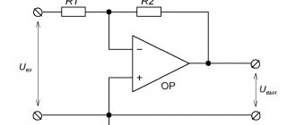
As I already said in one of the previous posts, I started publishing a series of articles about operational amplifiers. In the last article, I looked at two basic switching circuits (inverting and non-inverting) and some circuits using operational amplifiers. In this article I will consider such a topic as feedback.
To assemble a radio-electronic device, you can pre-make a DIY KIT kit using the link.
Why do you need feedback?
Unlike ideal operational amplifiers (op-amps), which have a uniform frequency response, that is, their gain does not change depending on the frequency of the input signal, real op-amps have a gain that decreases with increasing frequency of the amplified signal. In addition, in an op-amp, as the signal frequency increases, a phase shift occurs between the input and output signals, as a result of which, at some frequencies of the amplified signal, the circuit self-excites, that is, the amplifier turns into a generator. All this leads to a decrease in the quality indicators of electronic circuits.
One of the most common and effective ways to influence the quality parameters of electronic circuits with op-amps is the use of feedback (FE). It is worth noting that OS is widely used not only with op-amps, but also with many other electronic circuits, so everything that will be said about using OS with op-amps also applies to all other circuits with OS.
Feedback is defined as the connection between the output circuit of an amplifier and its input circuit, that is, when the amplified signal from the output of the amplifier is transmitted to its input through circuits that are specially introduced for this purpose (external feedback) or through circuits that are available in the amplifier for other purposes. functions (internal OS). The figure below shows the block diagram of a feedback amplifier
Block diagram of an amplifier with feedback.
The figure above shows the block diagram of an amplifier with gain K, which is covered by an external feedback circuit with gain β. The arrows in the diagram show the direction of the signal. Thus, part of the amplified signal from the output of the amplifier is supplied through the feedback circuit to the input of the amplifier, where it is added to the external signal. As a result, a total input signal appears at the amplifier input, which may be greater or less than the external signal.
The role of compensation in the feedback loop
The further away the selected system transition frequency is from the converter's natural cutoff frequency, the more stable its output voltage will be. In this case, it has a better gain and phase margin, but at the same time its response to disturbances is slower. A phase margin of approximately 45° provides good response with little transient and no ringing.
In addition, stability can be achieved by simply moving the system cutoff frequency to a safe zone. This is achieved by simply increasing the gain of the error amplifier over the entire operating frequency band. Thus, the phase shift of the error amplifier can be independent of frequency, which is achieved by adding compensation elements to the feedback circuit of the operational amplifier (Fig. 6).
Rice. 6. Uncompensated (left) and compensated (right) error amplifier
The values of the compensation components can be chosen so that the phase of the signal is reversed and adds phase margin at the point of the critical transition frequency, thereby increasing the stability of the converter. This allows the use of a lower damping output filter, thereby speeding up the response of the DC/DC converters during transients without the risk of excessive overshoot or spurious oscillation (Figure 7).
Rice. 7. Relationships between gain and phase in the compensated error amplifier circuit shown in Fig. 5
Additional explanations are given in Fig. 8.
Rice. 8. Compensated (solid line) in relation to the single-pole (shown in dotted line) characteristics (AFC and PFC) of the feedback loop for the circuit shown in Fig. 6
Here the dotted line shows the gain and phase versus frequency for an error amplifier with additional gain but no compensation. And the solid line shows the additional gain and phase shift obtained due to the compensation components.
The maximum possible phase shift that can be obtained through compensation is 180° (–90…+90°). In addition, to compensate for the zeros and poles of the output filter, an additional number of poles and zeros must also be included in the compensation circuit.
With a properly designed feedback loop, the response to a load dump or step change in load or input voltage (without any loss of stability in the feedback loop) can be accelerated by 3-4 times.
Types of feedback
If the sum of the amplitudes of the external signal and the signal of the feedback circuit turns out to be greater than the amplitude of the external signal, then this feedback circuit is called positive feedback (POS), and if the sum of the amplitudes of the external signal and the signal of the feedback circuit turns out to be less than the amplitude of the external signal, then such feedback called negative feedback (NFB).
By introducing OS, it is possible to quite significantly change the operating process and properties of the amplifier, which are determined both by the property of the amplifier and by the property of the OS circuit. The properties of the OS circuit are significantly influenced by its type, that is, the principle of its operation, which generally depends on the polarity and phase of the OS voltage, as well as the method of its connection to the input and output circuits of the amplifier.
There are four types of feedback:
- parallel voltage feedback.
- parallel current feedback.
- serial voltage feedback.
- Serial current feedback.
In addition, there is also mixed feedback, but due to the complexity of manufacturing and setting up, this type of feedback is not widely used.
Let's look at how each type of feedback is formed.
Determining feedback loop stability using the Laplace transform
An alternative to the experimental method of determining stability is the mathematical calculation of zeros and poles. To do this, we need to know the transfer function of the converter.
For the simple buck converter shown in Fig. 1, the transfer function is:
The parameter denoted as s here indicates that the transfer function variable is frequency dependent. The transfer function can be solved using the Laplace transform, but in order to understand this transform, we first need to consider the Fourier transform.
The Fourier transform is a special form of the Laplace transform. Fourier established that any periodic signal is the sum of sinusoidal signals of different frequencies, phases and amplitudes (Fourier series). Conversion is a transition from the time domain to the frequency domain (and vice versa). The result of the Fourier transform for a periodic signal is the equivalent of a Fourier series, or spectrum. In Fig. Figure 15 clearly shows the first six harmonics of a periodic square wave signal.
Rice. 15. Graphical representation of the Fourier series expansion for a rectangular waveform
The Fourier transform is the integral of a function with limits of integration from minus to plus infinity. This can be written as:
When displayed in the S-plane, the Fourier transform variable becomes equal to s = jω, and the result will be only imaginary (complex) variables.
The Laplace transform is an extended version of the Fourier transform. The Laplace transform variable is in the complex plane, and integration starts from zero rather than minus infinity. In this case, the time function F(t) is replaced by its image as a function of frequency F(s). This means that this transformation can be used to analyze stepwise or semi-infinite signals, such as a pulse or exponential decay sequence. The Laplace transform can be written as:
When moving to the S-plane, the Fourier transform variable is replaced by s = σ + jω.
Using the Laplace transform, one can mathematically model the feedback loop and generation of zeros and poles in the S-plane of the diagram. The vertical axis is imaginary and the horizontal axis is real. The higher or lower they move along the imaginary axis, the faster the oscillations occur. The further the movement along the negative real axis, the faster the decay, and the further the movement along the positive real axis, the faster the rise, which is explained in Fig. 16.
Rice. 16. A graph of the location of zeros and poles in the S-plane shows the corresponding typical timing diagrams of system behavior
The zeros always lie on the real axis. Complex conjugate pairs of poles in the left half of the S-plane combine to form a response that is a damped sinusoidal function of the form
where A and θ are the initial conditions, σ is the decay rate, and ω is the angular frequency in rad/s.
A pair of poles that lies on the imaginary axis ±jω (without a real component) generates oscillations with constant amplitude. The pole's distance from the origin indicates how the response decays. The closer the pole is to the origin, the lower the decay rate. If the pole is at zero, this means that we have a direct current system.
If the pole is in the right half-plane, the system is unstable (this corresponds to the concept of right-hand half-plane instability - RHP, described earlier).
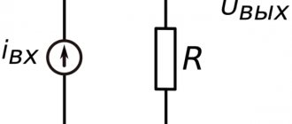
Parallel voltage feedback
Parallel voltage feedback is formed by connecting the input of the feedback circuit in parallel with the load resistance RH, and the output of the feedback circuit in parallel with the input of the amplifier.
Block diagram of parallel voltage feedback.
Thus, the input voltage of the OS circuit UСВ is equal to the output voltage on the load UН, and the output voltage of the OS circuit UOS is proportional to the sum of the currents of the input signal ISIG and the OS circuit IOC at the common input resistance of the amplifier circuit.
That is, this OS is formed by parallel connection of the input and output of the amplifier through the OS circuit. This type of OS is characterized by the fact that the effect of the OS decreases as the resistance of the load and the signal source decreases, and if the input or output is short-circuited, the action of this type of OS stops.
Q = K (C3 R1 / C23 R32)
K – gain; FP – frequency of a pair of poles implemented by the filter; Q is the quality factor of a pair of poles implemented by the filter.
With a value of Q>0.707, the amplifier's frequency response has an overshoot in the low-frequency region, which is undesirable. The values C3, C23, R1, R32 should be chosen so as to ensure the value of Q≤0.5 at which the filter implements a real pair of poles. The values indicated in the diagram correspond to the value Q = 0.36, at which a monotonic decline in the frequency response of the amplifier in the low-frequency region is guaranteed.
The negative impact of another drawback - the relatively small suppression of supply voltage ripple - is significantly weakened by the use of stabilized power supplies for input repeaters on VT1, VT4, HL1, HL2, R2-R4, R7, C4, C7.
The initial bias of the output buffer transistors is set using VT11, R15 and R17, which form the so-called base-emitter junction voltage multiplier circuit:
Parallel current feedback
Parallel current feedback is formed by connecting the input of the feedback circuit in parallel with the resistor RT, and the output of the feedback circuit is connected in parallel with the input of the amplifier.
Block diagram of parallel current feedback.
This type of OS is characterized by the following parameters: the input OS voltage UOC is proportional to the output current of the amplifier flowing through resistors RT and RH, and the output voltage of the OS circuit UOS is proportional to the sum of the currents of the input signal ISIG and the OS circuit IOC at the common input resistance of the amplifier circuit.
The effect of this type of feedback decreases with a decrease in the resistance of the signal source, the input resistance of the amplifier, as well as with a decrease in the resistance of the resistor RT or an increase in the load resistance. That is, if there is a short circuit at the input of the circuit and there is no load, this OS does not operate.
VceVT11 = VbeVT11 (1 + ( (R15 + R16) / R17) )
VceVT11 – voltage between the collector-emitter terminals; VbeVT11 – voltage between base-emitter pins.
The value of the voltage multiplier Vbe is set by R15 to approximately six, that is, the number of forward biased emitter junctions of the transistors used in the output buffer. To reduce the temperature drift of the quiescent current VT16, VT17 - include resistors R22, R23, R25-R28, R30, R31 in their emitter circuits. The choice of values of these resistors is a compromise between the stability of the quiescent current of powerful resistors and the efficiency of the amplifier.
R9, R10 are bypassed by C8, C9, are connected in parallel for alternating current and perform two functions simultaneously: they stabilize the quiescent current of VT5, VT6 and are the lower arm of the voltage divider of the common negative feedback circuit of the amplifier. The upper arm of the voltage divider of the OOOS circuit is formed by resistors R12, R13 connected in parallel with alternating current. The gain of the UMZCH can be calculated using the formula:
Serial voltage feedback
Serial voltage feedback is formed by connecting the input of the feedback circuit in parallel with the load resistance RH, and the output of the feedback circuit in series with the input of the amplifier.
Block diagram of an amplifier with a series voltage feedback circuit.
In serial voltage feedback, the input voltage UСВ is equal to the output voltage on the load UН. At the same time, the sum of the output voltage of the feedback circuit UOS and the voltage of the signal source USIG is equal to the input voltage of the amplifier UВХ.
Thus, the serial voltage feedback decreases its effect as the signal source resistance increases and the load resistance and output resistance of the amplifier decreases. In the event that there is a short circuit at the output, as well as in idle mode at the input, this type of OS ceases to operate.
Table 1:
| OUOST components | Matching Amplifier Components |
| VT1, VT2, VT3, VT4 | VT2, VT3, VT5, VT6 |
| Current source I1 | VT1, HL1, R2, R4, C4 |
| Current source I2 | VT4, HL2, R3, R7, C7 |
| Current mirror 1 | VT7, VT9, R8, R14 |
| Current mirror 2 | VT8, VT10, R11, R18 |
| Buffer | VT11-VT17, R15-R17, R19-R28, R30, R31, C13-C16 |
The inclusion of an integrator in the feedback circuit increases the order of the amplifier’s transfer function, turning it into a 2nd order high-frequency filter with the parameters:
Serial current feedback
Serial current feedback is formed by connecting the input of the feedback circuit in parallel with the resistor RT, and the output of the feedback circuit is connected in series with the signal source and the amplifier input.
Block diagram of an amplifier with serial current feedback.
Serial current feedback has the following characteristics. The input voltage of the OS circuit UCB is proportional to the output current of the amplifier ICB, which flows through resistors RH, RT and ROUT, and the output voltage of the OS circuit UOS together with the voltage of the signal source USIG constitutes the input voltage of the amplifier UВХ.
From the above it follows that with a decrease in resistances RH, RT and ROUT, as well as with an increase in the input resistance of the amplifier and the signal source, the effect of the series current feedback decreases. And in the absence of load and idling at the input of the circuit, this type of feedback is reduced to zero.
This article cannot contain all the information about feedback, so it only discusses diagrams of various types of feedback. The influence of the OS on the parameters of amplifying devices will be discussed in the next article.
Theory is good, but you need to practice it all practically. YOU CAN TRY HERE
Fig. 1 – functional diagram of a typical OUOST:
Mechanical translation of circuit solutions of analog ICs into discrete components does not give the expected results. IC components (transistors, resistors) manufactured in the same technological cycle and closely located on the chip have well-matched parameters and almost equal temperatures. The degree of consistency of discrete components of the same type is much lower, and their temperatures can differ significantly. With a diskette implementation of the current mirror, the predictability and stability of its parameters can be ensured only by including current-stabilizing resistors in the emitter circuits of the transistors. In the amplifier, the transmission coefficients of the current reflectors are chosen equal to two and are determined by resistances R8, R11, R14, R18. Resistors R5, R6, R9, R10 provide temperature stabilization of the quiescent current of transistors VT5, VT6.
Table 2 – SOI for various combinations of output power at frequencies of 1 kHz and 10 kHz:
| Test conditions | SOI (%) | ||
| F (kHz) | Pout (W) | Rload (Ohm) | |
| 1 | 7,5 | 8 | 0,00099 |
| 1 | 25 | 8 | 0,00198 |
| 1 | 15 | 4 | 0,00151 |
| 1 | 50 | 4 | 0,00229 |
| 10 | 7,5 | 8 | 0,00127 |
| 10 | 25 | 8 | 0,00216 |
| 10 | 15 | 4 | 0,00141 |
| 10 | 50 | 4 | 0,00290 |
Analysis of amplifier performance using OrCAD 9.2 under the following conditions:
- rated voltages of power supplies: ±27 V and ±15 V;
- quiescent current VT16, VT17 = 130 mA;
- amplifier load 4 ohms;
- capacitance C12 = 220 pF;
- the test signal sources have zero resistance.
Table 3 - Dependence of the main characteristics on the capacitance of the correction capacitor:
| Capacitance C12 (pF) | High passband frequency at -3 dB (MHz) | Phase stability margin (°) | Maximum load capacitance (pF) | Maximum rate of change of output signal (V/µs) | |
| growth | recession | ||||
| 51 | 27,09 | 70,44 | 1300 pF | 1388 | 1859 |
| 75 | 14,18 | 77,71 | 2200 pF | 953,4 | 982,3 |
| 100 | 10,11 | 80,89 | 4000 pF | 722,1 | 750,5 |
| 220 | 4,41 | 85,87 | ∞ | 336,8 | 339,7 |
| 330 | 2,93 | 87,17 | ∞ | 225,7 | 225,8 |
| 470 | 2,05 | 87,93 | ∞ | 158,5 | 158,4 |
Figure 7:
In Fig. 7 bold lines highlight conductors through which alternating or pulsating currents of significant magnitude flow. The point marked "A" is the reference power ground, which is connected to the signal ground points by a separate printed conductor (possibly several). Printed conductors of low-current power buses must begin at the connection point of the terminals of electrolytic capacitors C20, C21. It is desirable that these capacitors have a low equivalent series resistance (ESR) at high frequencies. The sealing points for the potential leads of ceramic capacitors C18, C10 should be located in close proximity to the connection points for the collector leads of transistors VT16, VT17. The sealing points for the terminals of ceramic capacitors C10, C11 should be located next to the connection points for the corresponding terminals of the pairs of resistors R8, R14 and R11, R18. The “grounded” terminals of all decoupling capacitors must be connected to the reference ground (point A in Fig. 7) by separate printed conductors of sufficient width and the minimum possible length.
In addition, when developing the amplifier design, the following recommendations must be taken into account:
- transistor VT11 must be mounted on the radiator of a powerful transistor VT16 (or VT17). The location of transistor VT11 on the radiator and the thermal resistance of the transistor body-radiator are selected experimentally using the method given below;
- It is advisable to place integrated voltage stabilizers ±15 V (not shown in Fig. 2) directly on the UMZCH printed circuit board. Recommended types of stabilizers KR1157EN15A, KR1179EN15;
- if it is not possible to place transistors VT16, VT17 so that their terminals are soldered directly into the printed circuit board, it is necessary to use bundles of the minimum possible length, consisting of three twisted conductors with a core cross-section of at least 0.5 mm2.
It is important to understand that the implementation of the listed design measures significantly weakens unwanted parasitic connections, but fundamentally cannot suppress them to a zero level. The negative impact of residual parasitic connections is, at a minimum, a distortion of the amplitude-frequency and transient characteristics of the amplifier. In many cases, the external manifestations of the action of parasitic connections (but not the parasitic connections themselves!) can be weakened by “brute force,” namely, by increasing the capacitance of the correction capacitor C12. However, this is only an apparent solution to the problem, since it comes at the cost of an inevitable deterioration in the dynamic characteristics of the amplifier: at a minimum, the frequency band narrows and the maximum rate of change of the output signal decreases. There is a common misconception that the deterioration in quality indicators caused by parasitic connections (design factors) is “attributed” to the amplifier circuitry, i.e. Essentially, an incorrect conclusion is drawn about the maximum capabilities of the UMZCH circuit design. Unfortunately, there is no amplifier testing technique that allows us to separately quantify the contributions of the “circuit” and “parasitic” components to the deterioration of the UMZCH parameters. The conclusion from the above is obvious: achieving high quality indicators of the UMZCH is possible only with a balanced quality of its circuit and design solutions.
K = 1 + Reqv1 / Reqv2
Reqv1 – equivalent resistance of resistors R12 and R13 connected in parallel; Reqv1 is the equivalent resistance of resistors R9 and R10 connected in parallel.
The dynamic characteristics of the amplifier are determined by the frequency properties and operating modes of the transistors, as well as the resistances R12, R13 of the OOOS circuit and the frequency correction capacitance C12. Variations in the gain of the UMZCH by synchronous changes in R9, R10, the bandwidth changes slightly. This is what makes an amplifier with current feedback fundamentally different from traditional UMZCHs, in which the product of the gain and the bandwidth is a constant value.
Setting up UM3CH comes down to performing three operations:
- setting the total quiescent current of the output buffer transistors to 80-150 mA using trimming resistor R15;
- installation of optimal thermal coupling of transistors VT11 and VT16;
- choosing the optimal capacitance of the frequency correction capacitor C12.
Before turning on the amplifier for the first time, it is necessary, firstly, to set the slider of the trimming resistor R15 to the lowest position according to the circuit, secondly, to ensure the maximum possible thermal coupling of transistors VT11, VT16 and thirdly, to install capacitor C12 with a nominal value of 430-620 pF in the circuit. It is convenient (without breaking the power circuit) to estimate the quiescent current of the output buffer transistors by the total voltage drop across resistors R22, R23, R25-R28, R30, R31, the equivalent resistance of which is 0.5 Ohm. The optimal thermal coupling of transistors VT11, VT16 corresponds to equality of currents:
Fig. 3 – Frequency response of the amplifier when varying the capacitance of the correction capacitor C12:
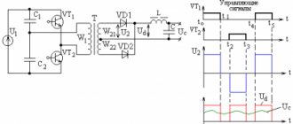
The response of the amplifier to the input influence is a sequence of pulses with the following parameters:
- voltage swing: 3 V;
- pulse repetition period: 1 µs;
- duration of rise and fall of pulses: 2;
The results obtained lead to the following conclusions:
- the dynamic characteristics of the UMZCH can predictably vary over a wide range by changing the frequency correction capacitance C12;
- in the audio frequency range, nonlinear distortions of UMZCH weakly depend on frequency (with an increase in frequency by an order of magnitude, the distortion increases by no more than 1.26 times);
- The power supply of the UMZCH can be supplied from unstabilized sources with a significant level of ripple.
As a result of the analysis, the following data was obtained:
- gain at 1 kHz: 10.1;
- output power at nonlinear distortion level: 72 W/4 Ohm;
- lower limit of bandwidth at 4.9 Hz: 3 dB;
- input impedance at 1 kHz: 12.9 kOhm;
- output impedance at 1 kHz: 0.000433 Ohm;
- penetration to the output of pulsations with a frequency of 100 Hz is about 1.3 mV/V with pulsations of one of the sources and about 0.13 mV/V with symmetrical antiphase pulsations of two sources.
Fig. 5 - Timing diagrams - amplifier response to input influence:
Simulation has shown that modern transistors of other types can be used in UMZCH. So, in particular, when replacing VT1, VT2, VT6, VT13 and VT3, VT4, VT5, VT12 with transistors KT6116A (2N5401) and KT6117A (2N5551), respectively, the main parameters of the UMZCH are even slightly improved. If the transfer coefficients of the current reflectors are set equal to unity (use resistors R14, R18 with a nominal value of 30 Ohms), then transistors VT7, VT9 and VT8, VT10 can also be replaced with transistors of types KT6116A and KT6117A. The situation is more complicated with the possibility of replacing powerful transistors VT16, VT17. Complementary transistors D44Н11, D45Н11 from Motorola are characterized by a unique combination of parameters:
- maximum permissible collector-emitter voltage – 80 V;
- maximum collector current – 10 A;
- limiting frequency of the current transfer coefficient is not less than 40 MHz.
The author was unable to find an adequate replacement for these transistors from domestic ones. However, with some deterioration in dynamic characteristics, powerful low-frequency transistors may well be used in UMZCH. A comparative analysis of the original circuit (Fig. 2) of the UMZCH and the version in which low-frequency transistors VT1b, VT17 of types 2N3055, MJ2955 (domestic analogs of KT819, KT818) were used showed the following:
- when using low-frequency transistors, deterioration of the frequency response (narrowing of the band, surge in the frequency response in the high-frequency region) occurs when the capacitance of the correction capacitor C12 is less than 220 pF;
- with a capacitance of capacitor C12 exceeding 220 pF, the dynamic characteristics (frequency response, maximum rate of change of the output signal, stability when operating with a capacitive load) of both circuit options are almost the same.
The potential capabilities of the amplifier can only be realized with an optimal printed circuit board (PCB) topology that minimizes parasitic electromagnetic couplings, which can have a significant negative impact on the characteristics of the UMZCH. Taking into account the specific features of the amplifier (relatively small voltage gain and low input resistance, high levels of output buffer currents, fairly wide bandwidth), we can conclude that the dominant types of parasitic coupling in UMZCH are:
- communication through the finite resistance of the common section of the “ground” bus;
- communication through internal resistance and connecting wires of power supplies.
The technique for minimizing parasitic connections through common sections of the ground bus is obvious: the topology of the PCB and the wired installation of the amplifier must prevent the flow of large currents of the output buffer and small currents of the input stages (input follower, current-voltage converter) through the same (common) sections " earth" tires. It should be noted, however. that the obviousness of the methodology does not at all mean the simplicity of the practical implementation of its recommendations. The weakening of parasitic connections through internal resistance and connecting wires of power supplies is achieved by the following measures:
- using low-frequency (oxide) and high-frequency (ceramic) decoupling capacitors;
- using separate (low-current and high-current) power buses for the current-voltage converter and output buffer;
- using stabilized voltages to power input voltage repeaters;
- connecting power supplies +27 V and -27 V with separate twisted pairs of wires of the minimum possible length.
The recommendations outlined are illustrated in Fig. 7, which conventionally depicts the elements and conductors that most influence the levels of parasitic connections.