Good day to all. In previous articles, I talked about the use of operational amplifiers in linear circuits, where the op-amp is covered by negative feedback, which allows you to build amplifiers whose parameters will be mainly determined by the op-amp's wiring elements. This article will talk about the use of op amps without feedback or even with positive feedback (POS).
To assemble a radio-electronic device, you can pre-make a DIY KIT kit using the link.
Bipolar power inverting amplifier circuit
The basic circuit of a bipolar power inverting amplifier looks like this:
Here we see two resistors and itself. We apply a signal to the input, and then remove the amplified signal from the output. As you can see, the non-inverting input of the op-amp is grounded. How does the scheme work? Here we see feedback. That is, the signal from the output is fed back to the input through resistor R2. Our amplifier is inverting, since the output signal is 180 degrees phase shifted relative to the input signal. This means that at the node where two resistors and the inverting input are connected, the output signal will arrive with a minus sign. Such feedback is called negative feedback ( NFC ) . It reduces the high gain of the op amp to the values we need.
In a NON-inverting amplifier, feedback is via voltage, and in an inverting amplifier, feedback is via current.
If you read the article about the op-amp, then you probably remember that if one of the inputs of the op-amp is connected to ground, then the other input has exactly the same potential. In this case, our non-inverting input is connected to ground, therefore, the inverting input will have exactly the same potential, that is, 0 Volts. Such an input is also called imaginary (virtual) earth . As Wikipedia says, “fake is false, counterfeit, false.”
The voltage gain of any amplifier is expressed by the formula
So what do we get in the end?
Input voltage from the formula above
But since our amplifier inverts the input signal, therefore, at the output we will have a voltage with a minus sign, that is, -Uout.
In this case, the current I2 will be expressed by the formula:
From here we find the gain
Since the input resistance of the inverting input is infinitely large, therefore, current will flow only through the circuit R1->R2. There cannot be two different currents in one branch, so it turns out that
As a result, our formula is reduced and we get
Voltage Comparator - Open Collector Output
Typically, the output of a voltage comparator is an open collector output.
The open collector output has negative polarity. This means that there is no positive signal at this output and the load must be connected between this output and the power supply.
In some circuits, a load (pull-up) resistor is connected to the output of the comparator in order to provide a high level signal arriving at the input of the next circuit element.
Operational amplifiers (op amps) such as LM324, LM358 and LM741 are not commonly used in electronic circuits as voltage comparators due to their bipolar outputs. However, these op amps can be used as voltage comparators by connecting a diode or transistor to the op amp output to create an open collector output.
Below is the operating logic of a comparator with an open collector output:
Current will flow through the open collector when the voltage at the (+) input is lower than the voltage at the (-) input. And accordingly, current will not flow through the open collector when the voltage at the input (+) is higher than the voltage at the input (-).
Example of an inverting amplifier
Let's see how our amplifier works in the Proteus electronic circuit simulator program. Here we are assembling a basic circuit with bipolar power supply
In Proteus it will look like this:
Here we took the value of resistors R2 = 10 kOhm and R1 = 1 kOhm, therefore, the gain of such a circuit will be equal to -10. The minus sign in this case simply inverts the amplified signal, which we see in the oscillogram below. The input signal is a pink waveform and the output signal is a yellow waveform. The output signal is in antiphase relative to the input, that is, it inverts it. Hence the name "inverting amplifier".
Three-phase drivers
Three-phase electric drive systems are often used to control electric motors. Naturally, such a power transistor control system can be implemented using three half-bridge drivers. But, despite all its obviousness, this solution turns out to be quite large; differences in the values of some parameters of drivers of different phases can lead to “distortions” of the system, a decrease in control efficiency and a decrease in the overall efficiency of the system.
Therefore, the IR company offers ready-made solutions to this problem, implemented in the form of three-phase drivers. The most interesting example of such a driver is the IRS26302D , shown in Figure 4. The driver has seven output channels controlled by independent inputs. Six channels are used to build the three-phase bridge itself, and the seventh channel can be used to implement a power factor corrector (PFC) or a protection and regeneration system.
Rice. 4. Typical connection diagram for a seven-channel three-phase driver
If the reader probably does not have any questions regarding the functionality of the cash register, then a description of the operation of the security system may be useful. So, when controlling a powerful motor with high mechanical inertia, when control actions are removed from the driver (to stop the motor), the motor can continue its rotation by inertia, thereby acting as an electricity generator - the potential of the system’s power bus will begin to increase. If the motor is powerful enough, the voltage can increase so much that it exceeds all permissible operating voltage levels of both the driver and the bridge transistors, which will lead to their breakdown and failure. To prevent such a situation, an additional seventh driver channel can be used. The microcircuit constantly monitors the value of the current on the power bus using a current-measuring resistor, and at the moment when a large reverse current in the bus is detected (situation of power generation by the motor), the transistor controlled by the seventh channel will open and begin to “drain” excess power on the protective diode ( or resistor assembly). If, instead of passively burning energy in the resistor module in the form of heat, you use a recuperator included in the circuit instead of these resistors, then you can store excess energy in batteries for its subsequent use (for example, when the engine is running at increased load).
Naturally, the family of three-phase drivers produced by IR is not limited to this one microcircuit. A more complete list of microcircuits indicating their key parameters is given in Table 4.
Table 4. Three-phase drivers and their key parameters
| Name | Number of channels | Bus voltage, V | Current Io+, mA | Current Io-, mA | Switching delay time of half-bridge arms nom., ns | Turn-on time Ton nom., ns | Turn-off time Toff nom., ns | Inverted inputs | Frame |
| IR3230S | 6 | 65 | 350 | 350 | — | 250 | 250 | LIN/HIN | 28 Lead SOIC |
| IRS2334M | 6 | 600 | 120 | 250 | 290 | 530 | 530 | LIN/HIN | 28-Lead MLPQ |
| IRS2334S | 6 | 600 | 120 | 250 | 290 | 530 | 530 | LIN/HIN | 20-Lead SOIC |
| IRS23365D | 6 | 600 | 180 | 380 | 275 | 530 | 530 | LIN/HIN | 48 Lead MLPQ |
| IR21363 | 6 | 600 | 200 | 350 | 290 | 425 | 400 | LIN/HIN | 28 or 44 Lead |
| IR21364 | 6 | 600 | 200 | 350 | 290 | 500 | 530 | LIN/HIN | 28 or 44 Lead |
| IR21365 | 6 | 600 | 200 | 350 | 290 | 425 | 400 | LIN/HIN | 28 or 44 Lead |
| IR21368 | 6 | 600 | 200 | 350 | 290 | 425 | 400 | LIN/HIN | 28 or 44 Lead |
| IRS2336 | 6 | 600 | 200 | 350 | 275 | 530 | 530 | LIN/HIN | 28 or 44 Lead |
| IRS23364D | 6 | 600 | 200 | 350 | 270 | 530 | 530 | — | 28 or 44 Lead |
| IRS2336D | 6 | 600 | 200 | 350 | 270 | 530 | 530 | LIN/HIN | 28 or 44 Lead |
| IRS26310DJ | 6 | 600 | 200 | 350 | 290 | 530 | 530 | — | 44 Lead PLCC |
| IR2130 | 6 | 600 | 250 | 500 | 2500 | 675 | 425 | LIN/HIN | 28 or 44 Lead |
| IR2131 | 6 | 600 | 250 | 500 | 700 | 1300 | 600 | — | 28 or 44 Lead |
| IR2132 | 6 | 600 | 250 | 500 | 800 | 675 | 425 | LIN/HIN | 28 or 44 Lead |
| IR2133 | 6 | 600 | 250 | 500 | 250 | 750 | 700 | LIN/HIN | 28 or 44 Lead |
| IR2135 | 6 | 600 | 250 | 500 | 250 | 750 | 700 | LIN/HIN | 28 or 44 Lead |
| IR2136 | 6 | 600 | 250 | 500 | 290 | 425 | 400 | LIN/HIN | 28 or 44 Lead |
| IRS2330 | 6 | 600 | 250 | 500 | 2000 | 500 | 500 | LIN/HIN | 28 or 44 Lead |
| IRS2330D | 6 | 600 | 250 | 500 | 2000 | 500 | 500 | LIN/HIN | 28 or 44 Lead |
| IRS2332 | 6 | 600 | 250 | 500 | 700 | 500 | 500 | LIN/HIN | 28 or 44 Lead |
| IRS2332D | 6 | 600 | 250 | 500 | 700 | 500 | 500 | LIN/HIN | 28 or 44 Lead |
| IR2233 | 6 | 1200 | 250 | 500 | 250 | 750 | 700 | LIN/HIN | 28 or 44 Lead |
| IR2235 | 6 | 1200 | 250 | 500 | 250 | 750 | 700 | LIN/HIN | 28 or 44 Lead |
| IR2238Q | 6 | 1200 | 350 | 540 | 1000 | 550 | 550 | HIN | 64 Lead MQFP |
| IRS26302DJ | 7 | 600 | 200 | 350 | 290 | 530 | 530 | LIN/HIN | 44 Lead PLCC |
Inverting amplifier output saturation
Let's imagine this situation. We have an input alternating voltage with an amplitude of 1 V. The gain is 50. According to our calculations, we should receive a signal with an amplitude of 50 V at the output. But how do we get 50 V if the power supply to our amplifier is, say, +-15 V? We will not be able to receive an amplified signal with an amplitude greater than 15 V. Although the typical voltage drop in the internal circuits of real op-amps is about 0.5-1.5 V. That is, the maximum signal swing that we can get in this case at the output will be 27-29 Volts.
Although at present there are op-amps that still allow you to receive +-Up at the output. This property of some op-amps is called Rail-to-Rail. Literally translated “from rail to rail” or “from tire to tire.” There are parameters such as Rail-to-Rail input. Here we can supply signals up to the input of the op-amp. Sometimes the datasheet stipulates whether this parameter can be approached from the negative or positive power bus. There is also a Rail-to-Rail output. Here at the output we can get the voltage +-Up. If the amplified output signal does not fit into this range, it will be clipped. This property of an op-amp is called output saturation . That is, we must always remember that if the amplitude of the signal exceeds + - Upit of the amplifier, then such a signal at the output will be cut off at this level.
Let's demonstrate this in the Proteus simulator. So, let's apply a sinusoidal signal with an amplitude of 1 V to the input, and make the gain 20 by selecting the necessary resistors. That is, according to our calculations, we should get a sine with an amplitude of 20 Volts. Let's look at the oscillogram
We fed a sinusoid to the input, but at the output we received a sinusoid with cut off tops and an amplitude of 14 V. One cell in this case is 2 V. As you can see, we cannot get a signal with an amplitude of more than +-Upit. Always remember this, especially when designing electronic devices.
Half Bridge Drivers
Most of the chips from the International Rectifier driver range contain two output channels in one package for controlling the upper and lower keys. These drivers control the input channels independently, which can be used to open both keys simultaneously, or dependently - this implies the impossibility of simultaneously opening the keys (even for a short period due to the built-in pause between switching keys - the so-called Dead-Time (DT)), which ensures the fundamental absence of through current through the keys. In the second case, the drivers are called Half-Bridge drivers.
The built-in Dead-Time mechanism ensures guaranteed closure of one power switch until the key in the opposite arm begins to open. A guarantee of reliable closing of the opposite transistor is a built-in circuit that controls the state of the keys, and the presence of a delay circuit that forms the period of time during which both transistors in the half-bridge arms are closed.
Most drivers of both types have a structure shown in Figure 2 using the example of a block diagram of the IRS2110 .
Rice. 2. Internal block diagram of IRS2110 driver
As can be seen from Figure 2, the control signals for the upper and lower switches are supplied through the corresponding inputs Hin and Lin to the Schmitt triggers, then through the “3OR-NOT” element to the level converters and PWM drivers. Thanks to the presence of logical “OR” elements, it is possible to block the driver’s operation using an input signal (Shut-Down), and the RS-flip-flops available at the input of the elements eliminate the uncertain state of the inputs after the supply voltage is applied to the device.
Input signals are compatible in levels with signals from microcircuits made according to TTL/CMOS technology standards. Some drivers interpret as a logical one an input signal whose level is at least 10% of the driver supply voltage (for example, IRS211x). Other drivers (for example, the IRS210x , IRS212x and IRS213x ) have a fixed voltage range corresponding to the transition state between logic levels. For the specified types of drivers, it corresponds to the interval 1.5...2 V.
The microcircuits provide the same time delay for the signal passage for both channels and have additional functionality - the ability to switch to an inactive state (if there is an SD input), separation of power and signal grounds, limiting the maximum operating current of transistors, etc. Typical driver connection diagrams are presented in Figure 3.
Rice. 3. Typical circuits for connecting half-bridge drivers: without Dead-Time (a) and with Dead-Time (b)
The range of half-bridge drivers in the IR portfolio is very wide. The following summary tables 2 and 3 provide information about the chips that are of greatest interest to the user.
Table 2. Half-bridge drivers without built-in Dead-Time function
| Name | Bus voltage, V | Current Io+, mA | Current Io-, mA | Turn-on time Ton nom., ns | Turn-off time Toff nom., ns | Inverted inputs | Separated signal and power “grounds” | Shutdown input (SD) | Frame |
| IRS2001M | 200 | 130 | 270 | 160 | 150 | — | PQFN 4 x 4 | ||
| IRS2001 | 200 | 290 | 600 | 160 | 150 | — | 8-Lead SOIC | ||
| IRS2011 | 200 | 1000 | 1000 | 60 | 60 | — | 8-Lead SOIC | ||
| IRS2110 | 500 | 2500 | 2500 | 130 | 120 | — | Yes | Yes | 16-Lead SOIC |
| IR25604 | 600 | 200 | 350 | 220 | 200 | LIN/HIN | 8-Lead SOIC | ||
| IRS2301 | 600 | 200 | 350 | 220 | 200 | — | 8-Lead SOIC | ||
| IRS2302 | 600 | 200 | 350 | 220 | 200 | — | 8-Lead SOIC | ||
| IRS26072D | 600 | 200 | 350 | 200 | 200 | — | 8-Lead SOIC | ||
| IRS2607D | 600 | 200 | 350 | 515 | 500 | — | 8-Lead SOIC | ||
| IRS2101 | 600 | 290 | 600 | 160 | 150 | — | 8-Lead SOIC | ||
| IRS2106 | 600 | 290 | 600 | 220 | 200 | — | 8-Lead SOIC | ||
| IRS21064 | 600 | 290 | 600 | 220 | 200 | — | 14-Lead SOIC | ||
| IRS2112 | 600 | 290 | 600 | 135 | 130 | — | Yes | Yes | 16-Lead SOIC |
| IRS21856 | 600 | 500 | 500 | 150 | 160 | LIN/HIN | 14-Lead SOIC | ||
| IRS2181 | 600 | 1900 | 2300 | 180 | 220 | — | 8-Lead SOIC | ||
| IRS21814 | 600 | 1900 | 2300 | 180 | 220 | — | Yes | Yes | 14-Lead SOIC |
| IRS21814M | 600 | 1900 | 2300 | 180 | 220 | — | Yes | Yes | PQFN 4 x 4 |
| IR25607 | 600 | 2500 | 2500 | 120 | 94 | LIN/HIN | 16-Lead SOIC | ||
| IRS2113 | 600 | 2500 | 2500 | 130 | 120 | — | Yes | Yes | 16-Lead SOIC |
| IRS2113M | 600 | 2500 | 2500 | 130 | 120 | — | Yes | Yes | PQFN 4 x 4 |
| IRS2186 | 600 | 4000 | 4000 | 170 | 170 | — | 8-Lead SOIC | ||
| IRS21864 | 600 | 4000 | 4000 | 170 | 170 | — | Yes | Yes | 14-Lead SOIC |
| IRS21867 | 600 | 4000 | 4000 | 170 | 170 | — | 8-Lead SOIC | ||
| IR2213 | 1200 | 2000 | 2500 | 280 | 225 | — | Yes | Yes | 16-Lead SOIC |
Table 3. Full Half Bridge Drivers (with Dead-Time)
| Name | Bus voltage, V | Current Io+, mA | Current Io-, mA | Switching delay time of half-bridge arms nom., ns | Turn-on time Ton nom., ns | Turn-off time Toff nom., ns | Inverted inputs | Separated signal and power “grounds” | Frame |
| IRS2003 | 200 | 290 | 600 | 520 | 680 | 150 | LIN | 8-Lead SOIC | |
| IRS2004 | 200 | 290 | 600 | 520 | 680 | 150 | — | 8-Lead SOIC | |
| IR25601 | 600 | 120 | 260 | 100 | 220 | 220 | LIN/HIN | 8-Lead SOIC | |
| IR25606 | 600 | 200 | 350 | 540 | 220 | 200 | LIN/HIN | 8-Lead SOIC | |
| IRS2509S | 600 | 200 | 350 | 530 | 750 | 250 | IN | 8-Lead SOIC | |
| IRS2608D | 600 | 200 | 350 | 530 | 250 | 250 | LIN | 8-Lead SOIC | |
| IR25602 | 600 | 210 | 360 | 520 | 680 | 150 | LIN | 8-Lead SOIC | |
| IRS2103 | 600 | 290 | 600 | 520 | 680 | 150 | LIN | 8-Lead SOIC | |
| IRS2104 | 600 | 290 | 600 | 520 | 680 | 150 | — | 8-Lead SOIC | |
| IRS2108 | 600 | 290 | 600 | 540 | 220 | 200 | HIN | 8-Lead SOIC | |
| IRS21084 | 600 | 290 | 600 | 540…5000 | 220 | 200 | HIN | Yes | 14-Lead SOIC |
| IRS2109 | 600 | 290 | 600 | 540 | 750 | 200 | — | 8-Lead SOIC | |
| IRS21091 | 600 | 290 | 600 | 540…5000 | 750 | 200 | — | 8-Lead SOIC | |
| IRS21094 | 600 | 290 | 600 | 540…5000 | 750 | 200 | — | Yes | 14-Lead SOIC |
| IRS2111 | 600 | 290 | 600 | 650 | 750 | 150 | — | 8-Lead SOIC | |
| IRS2304 | 600 | 290 | 600 | 100 | 150 | 150 | — | 8-Lead SOIC | |
| IRS2308 | 600 | 290 | 600 | 540 | 220 | 200 | — | 8-Lead SOIC | |
| IRS2183 | 600 | 1900 | 2300 | 400 | 180 | 220 | LIN | 8-Lead SOIC | |
| IRS21834 | 600 | 1900 | 2300 | 400…5000 | 180 | 220 | LIN | Yes | 14-Lead SOIC |
| IRS2184 | 600 | 1900 | 2300 | 400 | 680 | 270 | — | 8-Lead SOIC | |
| IRS21844 | 600 | 1900 | 2300 | 400…5000 | 680 | 270 | — | Yes | 14-Lead SOIC |
| IRS21844M | 600 | 1900 | 2300 | 400…5000 | 680 | 270 | — | Yes | PQFN 4 x 4 |
| IR2114 | 600 | 2000 | 3000 | 330 | 440 | 440 | — | Yes | 24 Lead SSOP |
| IR21141 | 600 | 2000 | 3000 | 330 | 440 | 440 | — | Yes | 24 Lead SSOP |
| IR2214 | 1200 | 2000 | 3000 | 330 | 440 | 440 | — | Yes | 24 Lead SSOP |
| IR22141 | 1200 | 2000 | 3000 | 330 | 440 | 440 | — | Yes | 24 Lead SSOP |
Bias Current and Output Bias
The inputs of a real op amp draw a small current called bias current . In English datasheets it is called Input Bias Current . If the input circuits of the op-amp are built on bipolar transistors, then such a bias current will be somewhere around several tens of nanoamps, in contrast to the op-amp, where the input circuits are built on field-effect transistors. In input circuits built on field-effect transistors, the bias current is estimated in tenths of picoamps. Therefore, the bias current is very important specifically for op-amps, whose input circuits are built on bipolar transistors.
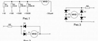
Why is bias current so important? Let's look at the diagram again
Even if we do not apply any signal to the input, we will still have some small constant voltage at the output. Why is this happening? The bias current is to blame for everything. It creates a voltage drop across the feedback resistor. In this case, it is resistor R2. And as you know, greater voltage drops at higher resistance. That is, if the value of resistance R2 is very large, then a large voltage will drop across it, which will go to the output of our op-amp.
Let's say the bias current is 0.1 μA, and resistor R2 = 1 MOhm, then what voltage drop will be across the resistor in this case? Let's remember Ohm's law: I=U/R, hence U=IR= 0.1 V. That is, at the output we will already have a constant voltage of 0.1 V! By applying a useful signal with a bias current of 0.1 μA to the input of such an amplifier, at the output this signal will be amplified and summed with a constant component of 0.1 V. In our case, the zero level is shifted. It’s clear in the figure below.
Comparator input offset voltage
Comparators are not perfect devices, and their performance may suffer from the effects of input offset voltage. The input offset voltage for many comparators can be only a few millivolts and can be ignored in most circuits.
Basically, the problem with input offset voltage occurs when the input voltage changes very slowly. The end result of an input offset voltage is that the output transistor does not turn fully on or off when the input voltage is close to the reference voltage.
The following diagram illustrates the effect of input voltage offset resulting from slowly changing input voltage. This effect increases with increasing transistor output current. Therefore, to reduce this effect, it is necessary to ensure the maximum resistance of resistor R4.
The effects of input offset voltage can be reduced by adding hysteresis to the circuit. This will cause the reference voltage to change when the comparator output goes high or low.
Ways to deal with bias current
In some cases, the bias current can be neglected if it does not greatly affect your signal requirements. But if, nevertheless, you are developing any precise device, where the output signal must strictly fit into the technical specifications, then in this case you can resort to the following methods:
1) Place a small value resistor in the feedback circuit.
At low resistance, low voltage drops. Consequently, the output will already have a lower constant voltage. The standard range of resistors is from a few kiloohms to 50 kOhms.
2) Introduce a compensating resistor into the circuit
In this case, it will be determined by the formula:
If, nevertheless, the output signal meets your expectations even without RC, then it is better not to install it, since any resistor introduces noise distortion into the signal. Why add noise to the circuit once again?
3) Use an op-amp with input circuits built on field-effect transistors , or select an op-amp with low bias currents, fortunately now the production technologies of such op-amps have made great strides forward.
Programming and Comparator
The comporator is not only used as part of an electrical circuit for PWM, etc., it is often used to create individual programs or their components. For example, the device is often used to create java collections.
- To work, you will need a special Maven program. First, you need to create a project; for full operation, you need an Internet connection. Create a new project, select two components in the structure: comparator and pojo. Availability is checked using the JUnit 4.11 utility;
- Install pom.xml and create a new file. Interrupting the process is unacceptable, so it is very important to save at every stage. Afterwards, a POJO is created and configured, where the necessary settings are specified. The parameters depend on the requirements for a particular library. This could be dates of birth, general information about accommodation, etc.;
- And only after that a comparator is created. This is a class that is used to verify data and distribute it to the required folders. Using this class is necessary if you need to sort certain information according to specified parameters (colors, sizes, dates). This ensures data protection and classification according to a certain principle.
You can buy a ready-made comparator at any radio equipment and electrical equipment store. The price of the device varies depending on its purpose and the number of channels.
Single-supply inverting amplifier
In some cases, we even sometimes need to move the null level to a higher "pedestal" so that we can fully amplify the signal when it comes to a single supply. Working with unipolar power supply is always easier and more convenient than working with bipolar power supply. Therefore, in this case it is necessary to raise the zero level to some pedestal in order to fully amplify the alternating signal. That is, add a constant component to the signal. In this case, the diagram will take a slightly different form:
As you can see, we are now powering our op-amp with single-supply power. What happens if we connect the non-inverting output to ground?
That is, we got a basic inverting amplifier circuit, but only with single-pole power supply. Let's simulate such a circuit. The gain in this case will be equal to -10, since we took the ratio of resistors 10 kilo-ohms and 1 kilo-ohms. I drive a signal with an amplitude of 1 V to the input.
What do we end up with on the virtual oscilloscope?
As you can see, in this case the amplified half-wave of the signal is cut out completely. This is understandable, since our supply voltage is unipolar and it is impossible to break the “floor” of zero potential. But there is one trick you can do: raise the “floor level” and give the signal room to spread.
In this case, we need to add Ucm in order to raise the signal above the “floor” level. But not everything is so simple, dear friends!
Here a more cunning formula will be used, and not just a voltage boost. The approximate formula looks like this:
So we want to boost our signal completely without clipping. What should be the value of Uout? It should have a value of half Upit so that the signal goes back and forth without cutting. But the gain must also be taken into account, otherwise the output will become saturated, as we wrote about above.
In our case, we want to increase the signal amplitude of 1 V by 10 times. That is, Upit must be at least 20 Volts. Since op-amps support single-pole power supply up to 32 V, let’s set Upit = 30 V for beauty. Let’s calculate Ucm:
We check the simulation, everything is ok!
As you can see here, the yellow output signal rose above the zero level and amplified without distortion. In this case, the yellow signal is the sum of a constant voltage and an alternating sinusoidal signal.
That is, it turned out something like this:
Is it good or bad when an alternating signal has a constant component, that is, a constant voltage? In some cases this is bad because the signal is difficult to use and is therefore most often driven through a capacitor since it only allows AC current to pass through and blocks DC from passing through. Better yet, install a filter from a differentiating circuit, with which you can cut off unnecessary frequencies.
Purpose
Why do you need a comparator and how to use it without an amplifier? In most cases, this device is used in simple computer circuits where it is necessary to compare incoming voltage signals. This can be a charger for a laptop or phone, a scale (mass meter), an AVR mains voltage sensor, a timer (composer type lm 358, microcontroller, etc. It is also used by various integrated circuits to control input pulses, providing communication between the signal source and its destination center.
Photo - comparators for computer
The most popular example is the Shimmer trigger comparator. It operates in multi-channel mode, which means it can compare a large number of signals. In particular, this trigger is used to restore a digital signal that distorts communication depending on the voltage level and distance of the power source.
This is an analogue of a standard comparator, just with more advanced functionality, which provides measurement of several incoming signals.
Photo - op-amp comparator
There is also a roughness comparator. This is a device that helps to visually determine the condition of a surface that has already been treated. The use of this device is justified by the need to determine the tolerances of previously processed surfaces.
Current Measurement Drivers
When using the above integrated drivers, the question of controlling the current consumed by the load remains open. If the driver IC has a current monitoring function, then, as a rule, it simply reports the occurrence of a malfunction using an additional error output, without deciphering the cause of its occurrence. One of the causes of an emergency may be an overcurrent of the output stage.
To control the current consumed by the load, International Rectifier produces integrated circuits that allow this function to be implemented. Figure 5 shows circuits for monitoring the current consumed by the load on a chip combined with a driver (a) and a specialized current measuring chip (b).
Rice. 5. Examples of turning on drivers that control the current in the load
IR22771 microcircuits are widely used in motor control and are connected individually to each phase. The microcircuit is not a driver in the classical sense, because does not control output transistors, but only provides current measurement and generates control actions for the central control unit (most often a DSP controller).