An operational amplifier (op-amp) is a fundamental element of modern analog electronics. Thanks to its excellent characteristics and ease of calculation, op-amps are very easy to use. Operational amplifiers are also called differential amplifiers because they can amplify the voltage difference across the inputs.
Operational amplifiers are produced as ready-made microcircuits, sometimes one at a time, and sometimes several pieces in one package. There are many types of operational amplifiers, which differ in technical parameters, which ultimately affects the feasibility of use in specific circuits.
In theory, the operational amplifier has ideal parameters. In practice, their parameters tend to be ideal, but still do not reach them. Using the concept of an "ideal" op amp helps simplify the calculations.
These ideal parameters are:
- infinitely large gain with open feedback loop;
- infinitely wide band of transmitted frequencies;
- infinitely large input impedance;
- impedance equal to zero;
- the output voltage is zero when the input voltages are equal.
As you can see, such parameters cannot be fully ensured, but from year to year the op amps are actually getting closer and closer to the ideal.
There are several basic operational amplifier circuits:
- inverting
- non-inverting
- subtraction
- addition
- differentiation
- integration
- voltage repeater
- analog comparator
What is an operational amplifier
An op-amp is an integrated circuit (IC), the main purpose of which is to amplify the value of direct current. It has only one output, which is called differential. This output has a high signal amplification factor (Kу). Op-amps are mainly used when constructing circuits with negative feedback (NFB), which, with the main gain characteristics, determines the K of the original circuit. Op-amps are used not only in the form of individual ICs, but also in various blocks of complex devices.
The op-amp has 2 inputs and 1 output, and also has pins for connecting a power source (PS). The operating principle of an operational amplifier is simple. There are 2 rules taken as a basis. The rules describe simple IC operation processes that occur in an op-amp, and how the IC works is clear even to dummies. At the output, the voltage difference (U) is 0, and the op-amp inputs consume almost no current (I). One input is called non-inverting (V+) and the other is inverting (V-). In addition, the op-amp inputs have high resistance (R) and consume virtually no I.
The chip compares the U values at the inputs and produces a signal, pre-amplifying it. Ku op-amp has a high value, reaching 1,000,000. If a low U is supplied to the input, then at the output it is possible to obtain a value equal to U of the power source (Uip). If U at the V+ input is greater than at V-, then the output will have a maximum positive value. When the inverting input is powered with positive U, the output will have a maximum negative voltage.
The main requirement for op-amp operation is the use of a bipolar power supply. It is possible to use a unipolar power supply, but the capabilities of the op amp are greatly limited. If you use a battery and take its positive side as 0, then when measuring the values you will get 1.5 V. If you take 2 batteries and connect them in series, then U will add up, i.e. the device will show 3 V.
Operational amplifier in subtraction circuit (differential amplifier)
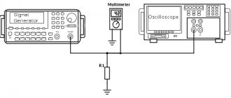
Another type of op amp circuit is a differential amplifier, which produces the difference between two input signals, which can then be amplified. The graph below shows how the system works.
The following circuit allows you to implement this operation of the operational amplifier:
The scheme is more complex compared to the previous ones. To calculate the output voltage, apply the formula:
The first part of the equation is the gain (or attenuation), and the second part is the difference between the two voltages.
Types and symbols on the diagram
With the development of electrical circuitry, operational amplifiers are constantly being improved and new models appear.
Classification by areas of application:
- Industrial ones are a cheap option.
- Precision (precise measuring equipment).
- Electrometric (low value of Iin).
- Micropower (low power consumption).
- Programmable (currents are set using external I).
- Powerful or high-current (giving a higher I value to the consumer).
- Low voltage (operate at U<3 V).
- High voltage (designed for high U values).
- Fast (high slew rate and amplification frequency).
- Low noise.
- Sound type (low harmonic distortion).
- For bipolar and unipolar type of electrical supply.
- Difference (capable of measuring low U with high noise). Used in shunts.
- Ready-made amplification stages.
- Specialized.
Based on input signals, op-amps are divided into 2 types:
- With 2 entrances.
- With 3 inputs. Input 3 is used to expand functionality. Has internal OOS.
The operational amplifier circuit is quite complex, and there is no point in manufacturing it, and the radio amateur only needs to know the correct circuit for connecting the operational amplifier, but for this he must understand the decoding of its pins.
Basic designations of IC pins:
- V+ is a non-inverting input.
- V- - inverting input.
- Vout - output. Vs+ (Vdd, Vcc, Vcc+) - positive terminal of the IP.
- Vs- (Vss, Vee, Vcc-) - minus IP.
Almost any op-amp has 5 pins. However, some varieties may lack V-. There are models that have additional pins that expand the capabilities of the op-amp.
It is not necessary to mark the power pins, because this increases the readability of the diagram. The power output from the positive terminal or pole of the power supply is located at the top of the circuit.
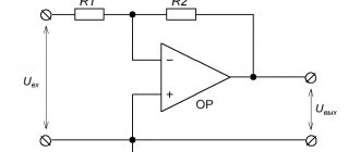
Inverting amplifier circuit
This is the basic circuit in which the op-amp operates. The operation of an operational amplifier is characterized not only by amplification (or attenuation) of the input signal, but also by changing its phase. Gain is denoted by the letter k. The graph below shows the effect of the op amp in this circuit:
Blue is the input signal graph and red is the output signal graph, with the system gain being 2 (k=2). As can be seen, the amplitude of the output signal is twice as high as the amplitude of the input signal, and it can also be seen that the signal is inverted.
The circuit of such an amplifier is quite simple, and is shown in the following figure:
This circuit proves why op amps are so popular. In order to calculate the values of the elements, we just need to use the following formula:
As you can see, resistor R3 does not affect the gain of the circuit, and one could do without it by connecting the positive input of the amplifier to the negative of the power supply. In this case, resistor R3 is used as protection.
Main characteristics
Op-amps, like other radio components, have TX, which can be divided into types:
- Amplifiers.
- Input.
- Weekend.
- Energy.
- Drifting.
- Frequency.
- Performance.
Gain is the main characteristic of an op-amp. It is characterized by the ratio of the output signal to the input signal. It is also called amplitude or transfer TX, which is presented in the form of dependence graphs. The input values include all quantities for the op-amp input: Rin, bias currents (Icm) and shift (Iin), drift and maximum input differential U (Udiffmax). Icm is used to operate the op-amp at the inputs. Iin is needed for the operation of the input stage of the op-amp. Iin shift - difference Icm for 2 input semiconductors of the op-amp.
When constructing circuits, you need to take these I into account when connecting resistors. If Iin is not taken into account, this can lead to the creation of a differential U, which will lead to incorrect operation of the op-amp. Udiffmax - U, which is supplied between the inputs of the op-amp. Its value characterizes the elimination of damage to the semiconductors of the differential stage.
For reliable protection, 2 diodes and zener diodes are connected back-to-back between the inputs of the op-amp. Differential input R is characterized by the R between two inputs, and common-mode input R is the value between the 2 op-amp inputs that are combined and ground (ground). The output parameters of the op amp include output R (Rout), maximum output U and I. The Rout parameter should be smaller in value to provide better gain characteristics.
To achieve a small Rout, you need to use an emitter follower. Iout changes with the help of collector I. Energy TX is estimated by the maximum power that the op-amp consumes. The reason for the incorrect operation of the op-amp is the spread in the characteristics of the semiconductors of the differential amplifier stage, which depends on temperature indicators (temperature drift). The frequency parameters of the op-amp are basic. They help to amplify harmonic and pulse signals (speed).
The op-amp IC of general and special types includes a capacitor that prevents the generation of high-frequency signals. At frequencies with low values, the circuits have a large coefficient Ku without feedback (OS). With OS, non-inverting switching is used. In addition, in some cases, for example, in the manufacture of an inverting amplifier, the OS is not used. In addition, the op-amp has dynamic characteristics:
- Slew rate of Uout (CH Uout).
- Settling time for Uout (op-amp response when U jumps).
Bias current
The op amp inputs have extremely high impedances. That is, the input currents flowing into or out of the op amp's two input signal pins are extremely small. For most purposes of analyzing op-amp circuits, we treat them as if they weren't there at all. We analyze the circuit as if the current entering or exiting the input pins were absolute zero.
However, this idyllic picture is not entirely true. Op-amps, especially op-amps with bipolar transistors at their inputs, must pass some current through their input pins in order for their internal circuits to be properly biased. These currents are logically called displacement currents. Under certain conditions, op amp bias currents can cause problems. The following diagram illustrates one of these problematic conditions:
Amplification of the thermocouple signal
At first glance, we don't see any obvious problems with this scheme. A thermocouple producing a small voltage proportional to the temperature (in fact, the voltage is proportional to the temperature difference between the sensing junction and the "reference" junction formed by connecting the thermocouple's alloy wires to the copper wires leading to the op-amp) drives the op-amp either positive or negative. in the negative direction. In other words, it is a kind of comparator circuit that compares the temperature between the junction at the end of the thermocouple and the reference junction (near the op-amp). The problem is this: the wire loop formed by the thermocouple does not provide a path for both input bias currents, since both currents are trying to take the same path (either into or out of the op-amp).
This comparator circuit
will not work
For this circuit to work properly, we must connect one of the input wires to ground, thus providing a path to (or from) the ground point for both currents:
This comparator circuit
will work
. This problem is not necessarily obvious, but it is very real!
Input bias currents can cause problems in another way: unwanted voltage drops across circuit resistances. Let's take the following diagram as an example:
Effect of input bias current on voltage follower operation
We expect a voltage follower circuit such as the one above to accurately reproduce the input voltage at its output. But what about the resistance in series with the input voltage source? If there is any bias current through the non-inverting (+) input, it will cause some voltage drop across Rin, so the voltage at the non-inverting input will not correspond to the actual value of Vin. Bias currents are usually in the microampere range, so the voltage drop across Rin will not be very large. One example of an application where the input resistance (Rin) can be very large is one that has pH probe electrodes where one electrode contains an ion-permeable glass barrier (a very poor conductor with resistance in the millions of ohms).
If we were actually building an op amp circuit to measure the voltage at a pH electrode, we would probably want to use an op amp with FET or MOSFET inputs, instead of an op amp with BJT inputs (for decrease the input bias current). But even then, there may still be small offset currents that can cause measurement errors, so we must find some way to reduce them through good design.
One way to do this is based on the assumption that the two input bias currents will be the same. In fact, they are often close to being the same, the difference between them being called the input bias current. If they are the same, then we should be able to remove the effect of the voltage drop across the input resistance by inserting a resistance of equal magnitude in series with the other input, for example:
Eliminating the influence of voltage drop across the input impedance
By adding additional resistance to the circuit, the output voltage will be closer to Vin than before, even if there is some offset between the two input currents.
For both the inverting amplifier circuit and the non-inverting amplifier circuit, a compensating resistor is placed in series with the non-inverting (+) input to compensate for voltage drops in the divider circuit due to the bias current.
Installing a compensating resistor in a non-inverting amplifier circuit
Installing a compensating resistor in the inverting amplifier circuit
In either case, the value of the compensating resistor is determined by calculating the parallel resistance R1 and R2. Why is the value equal to the parallel equivalent of R1 and R2? When using the superposition theorem to determine how much voltage drop will be created by the bias current of the inverting (-) input, we treat the bias current as if it were coming from a current source inside the op-amp and shorting out all voltage sources (Vin and Vout). This gives two parallel paths for the bias current (through R1 and through R2, both to ground). We want to duplicate the effect of the bias current on the non-inverting (+) input, so the value of the resistor we choose to insert in series with this input must be equal to R1 in parallel with R2.
A related problem that students sometimes experience when learning op-amp circuit design is caused by the power supply not being connected to a common ground. For the op amp to operate properly, it is necessary that some pin of the DC power supply be common to the ground point of the input signal(s). This provides a complete path for the bias currents, the feedback current(s), as well as the (output) load current. Take for example the following diagram showing a power supply properly connected to ground:
Negative feedback with a voltage divider using the example of an operational amplifier model
Here, the arrows indicate the path of current through the power supply batteries, both to power the internal circuitry of the op-amp (the "potentiometer" inside it that controls the output voltage) and to power the feedback loop of resistors R1 and R2. Let's assume that the ground point of this "split" DC power supply has been removed. The effect of this will be enormous:
Negative feedback with a voltage divider using an operational amplifier model as an example.
The midpoint of the ground at the power source has been removed. Connecting the power supply to ground is mandatory for the circuit to work!
No electrons can flow into or out of the op-amp's output pin because the path to the power supply ends in a "dead end". Thus, no electrons flow through either the ground point to the left of R1 or through the feedback loop. This effectively renders the op amp useless: it can neither support current through the feedback loop nor through the ground-connected load, since there is no connection at any point of the power supply to ground.
Bias currents are also stopped because they rely on a path to the power supply and back to the input source through ground. The following figure shows the bias currents (only) as they flow through the input pins of the op amp, through the base pins of the input transistors, and ultimately through the power supply pin(s) and back to ground.
Paths for input bias currents in an op-amp circuit.
The paths of bias currents are shown through the power supply.
Without a ground reference point at the power supply, bias currents will not have a full path through the circuit and will be stopped. Since bipolar transistors are current controlled devices, this also renders the op amp input stage useless, as both input transistors will be forced into cutoff mode due to the complete lack of base current.
Summary
- Op-amp inputs typically conduct very small currents, called bias currents, required to properly bias the first transistor amplifier stage in the op-amp circuit. Bias currents are not large in magnitude (in the microamp range), but are large enough to cause problems in some applications.
- The bias currents at both inputs must have paths to flow to one of the power supply's "rails" or to ground. It is not enough to simply provide a conductive path from one input to another.
- To eliminate any offset voltages caused by bias current flowing through the resistors, simply add an equivalent resistor in series with the other input of the op-amp (called a compensating resistor). This corrective measure is based on the assumption that the two input bias currents will be equal.
- Any disparity between bias currents in an op-amp constitutes what is called input bias current.
- For the op amp to operate properly, it is important that there is a ground reference at some pin of the power supply to form complete paths for the bias current, feedback current, and load current.