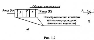
A diode is one of the types of devices designed on a semiconductor basis. It has one pn junction, as well as anode and cathode terminals. In most cases, it is designed for modulation, rectification, conversion and other actions with incoming electrical signals.
Principle of operation:
- An electric current acts on the cathode, the heater begins to glow, and the electrode begins to emit electrons.
- An electric field is formed between the two electrodes
- If the anode has a positive potential , then it begins to attract electrons to itself, and the resulting field is a catalyst for this process. In this case, an emission current is generated.
- Between the electrodes, a negative spatial charge is formed, which can interfere with the movement of electrons. This happens if the anode potential is too weak. In this case, some of the electrons are unable to overcome the influence of the negative charge, and they begin to move in the opposite direction, returning to the cathode again.
- All electrons that reach the anode and do not return to the cathode determine the parameters of the cathode current. Therefore, this indicator directly depends on the positive anode potential.
- The flow of all electrons that were able to get to the anode is called the anode current, the indicators of which in the diode always correspond to the parameters of the cathode current. Sometimes both indicators can be zero; this happens in situations where the anode has a negative charge. In this case, the field that arises between the electrodes does not accelerate the particles, but, on the contrary, slows them down and returns them to the cathode. The diode in this case remains in a locked state, which leads to an open circuit.
Device
Below is a detailed description of the diode structure; studying this information is necessary for further understanding of the principles of operation of these elements:
- The housing is a vacuum cylinder that can be made of glass, metal or durable ceramic varieties of material.
- inside the cylinder . The first is a heated cathode, which is designed to ensure the process of electron emission. The simplest cathode in design is a filament with a small diameter, which heats up during operation, but today indirectly heated electrodes are more common. They are cylinders made of metal and have a special active layer capable of emitting electrons.
- Inside the indirectly heated there is a specific element - a wire that glows under the influence of electric current, it is called a heater.
- The second electrode is the anode, it is needed to receive the electrons that were released by the cathode. To do this, it must have a potential that is positive relative to the second electrode. In most cases, the anode is also cylindrical.
- Both electrodes of vacuum devices are completely identical to the emitter and base of the semiconductor variety of elements.
- Silicon or germanium is most often used to make a diode crystal One of its parts is p-type electrically conductive and has a deficiency of electrons, which is formed by an artificial method. The opposite side of the crystal also has conductivity, but it is n-type and has an excess of electrons. There is a boundary between the two regions, which is called a pn junction.
Such features of the internal structure give diodes their main property - the ability to conduct electric current in only one direction.
Advantages of a Darlington pair
A Darlington pair has several advantages over a standard single transistor. Here are some of them:
- It provides very high current gain than a standard single transistor
- It provides very high input impedance or good impedance conversion.
- They can be two separate transistors or supplied in one package.
- Simple and convenient circuit configuration as only a few components are used.
- In the case of a photodarlington pair, the external noise is much less compared to a phototransistor with an external amplifier.
Purpose
Below are the main areas of application of diodes, from which their main purpose becomes clear:
- Diode bridges are 4, 6 or 12 diodes connected to each other, their number depends on the type of circuit, which can be single-phase, three-phase half-bridge or three-phase full-bridge. They perform the functions of rectifiers; this option is most often used in automobile generators, since the introduction of such bridges, as well as the use of brush-collector units with them, has made it possible to significantly reduce the size of this device and increase its reliability. If the connection is made in series and in one direction, this increases the minimum voltage required to unlock the entire diode bridge.
- Diode detectors are obtained by combining these devices with capacitors. This is necessary so that it is possible to isolate low-frequency modulation from various modulated signals, including the amplitude-modulated variety of the radio signal. Such detectors are part of the design of many household appliances, such as televisions or radios.
- Ensuring protection of consumers from incorrect polarity when switching on circuit inputs from occurring overloads or switches from breakdown by electromotive force that occurs during self-induction, which occurs when the inductive load is turned off. To ensure the safety of circuits from overloads that occur, a chain is used consisting of several diodes connected to the supply buses in the reverse direction. In this case, the input to which protection is provided must be connected to the middle of this chain. During normal operation of the circuit, all diodes are in a closed state, but if they have detected that the input potential has gone beyond the permissible voltage limits, one of the protective elements is activated. Due to this, this permissible potential is limited within the permissible supply voltage in combination with a direct drop in the voltage on the protective device.
- Switches based on diodes are used to switch high-frequency signals. Such a system is controlled using direct electric current, high-frequency separation and the supply of a control signal, which occurs due to inductance and capacitors.
- Creation of diode spark protection . Shunt-diode barriers are used, which provide safety by limiting the voltage in the corresponding electrical circuit. In combination with them, current-limiting resistors are used, which are necessary to limit the electric current passing through the network and increase the degree of protection.
Read also: Knives photo drawings drawings
Checking bipolar types
Below is a diagram for checking npn, pnp transistors with a tester, after which we will describe the procedure point by point.
The bipolar transistor is equipped with pn lines - conventionally, these are diodes, or rather, 2 of them located oppositely, the point of their intersection is the “base”.
One conditional diode is designed with base/collector contacts, the other with base/emitter contacts. For analysis, just look at the contrast. (directly and back) of the indicated areas: if there are no problems there, then the part is without flaws.
Do-it-yourself testing without soldering a bipolar pnp, npn transistor involves testing 3 combinations of legs:
pnp option
Structures (types) are shown by the arrow emitting. section: pnp/npn (to/from the base). Let's start by checking the first option. We open the PNP part by applying negative voltage to the base. On the multimeter, we set the selector to measure Ohms to o; it is also possible to set it to “continuity”.
The vein “−” (black) is on the base leg. Plus (red) - alternately to collect., emitter. If the areas are not damaged, they will display about 500–1200 Ohms.
Next we will describe how to ring the reverse resistance: “+” - to the base, “−” - to the call. and emits. High resistance should be displayed. on both pn sites. We now have “1”, that is, for the frame set to “2000” the value exceeds 2000. This means that there are 2 transitions without breaks, the product is in good working order.
It will be interesting➡ Instrumentation mechanic: professional features and difficulties
Similarly, as described, you can test the transistor for serviceability without removing it from the circuit. Less commonly, there are assemblies where substantial shunting is applied to the transitions, for example, with resistors. Then, if too low resistance is displayed, the part will need to be desoldered.
npn structure
Npn elements are checked in the same way, only the “+” probe goes to the base from the tester.
Symptoms of a problem
If the resistance (direct and reverse) of one of the sections (pn) tends to infinity, that is, at o and above on the display “1”, which means that this section has a break, the transistor is unusable. If “0” means the product is also flawed, the area is broken. Direct cont. there should be 500–1200 ohms.
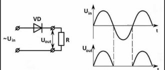
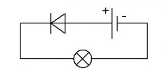
Direct diode connection
The pn junction of the diode can be affected by voltage supplied from external sources. Indicators such as magnitude and polarity will affect its behavior and the electrical current conducted through it.
Below we consider in detail the option in which the positive pole is connected to the p-type region, and the negative pole to the n-type region. In this case, direct switching will occur:
- Under the influence of voltage from an external source, an electric field will be formed in the pn junction, and its direction will be opposite to the internal diffusion field.
- The field voltage will decrease significantly, which will cause a sharp narrowing of the blocking layer.
- Under the influence of these processes, a significant number of electrons will be able to freely move from the p-region to the n-region, as well as in the opposite direction.
- The drift current indicators during this process remain the same, since they directly depend only on the number of minority charged carriers located in the pn junction region.
- Electrons have an increased level of diffusion, which leads to the injection of minority carriers. In other words, in the n-region there will be an increase in the number of holes, and in the p-region an increased concentration of electrons will be recorded.
- The lack of equilibrium and an increased number of minority carriers causes them to go deep into the semiconductor and mix with its structure, which ultimately leads to the destruction of its electrical neutrality properties.
- In this case, the semiconductor
Diode reverse connection
Now we will consider another method of switching on, during which the polarity of the external source from which the voltage is transmitted changes:
- The main difference from direct connection is that the created electric field will have a direction that completely coincides with the direction of the internal diffusion field. Accordingly, the barrier layer will no longer narrow, but, on the contrary, expand.
- The field located in the pn junction will have an accelerating effect on a number of minority charge carriers, for this reason, the drift current indicators will remain unchanged. It will determine the parameters of the resulting current that passes through the pn junction.
- As the reverse voltage , the electric current flowing through the junction will tend to reach its maximum. It has a special name - saturation current.
- In accordance with the exponential law , with a gradual increase in temperature, the saturation current indicators will also increase.
Forward and reverse voltage
The voltage that affects the diode is divided according to two criteria:
- Direct voltage is the one at which the diode opens and direct current begins to flow through it, while the resistance of the device is extremely low.
- Reverse voltage is one that has reverse polarity and ensures that the diode closes with reverse current passing through it. At the same time, the resistance indicators of the device begin to increase sharply and significantly.
This leads to an increase in the parameters of the forward current passing through the diode. When this device is closed, virtually the entire voltage is applied to it, for this reason the reverse current passing through the diode is insignificant, and the transition resistance reaches peak parameters.
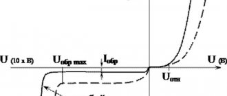
Diode operation and its current-voltage characteristics
The current-voltage characteristic of these devices is understood as a curved line that shows the dependence of the electric current flowing through the pn junction on the volume and polarity of the voltage acting on it.
Such a graph can be described as follows:
- The axis is located vertically: the upper area corresponds to the forward current values, the lower area to the reverse current parameters.
- Horizontal axis: The area on the right is for forward voltage values; area on the left for reverse voltage parameters.
- The direct branch of the current-voltage characteristic reflects the passing electric current through the diode. It is directed upward and runs in close proximity to the vertical axis, since it represents the increase in forward electric current that occurs when the corresponding voltage increases.
- The second (reverse) branch corresponds to and displays the state of the closed electric current, which also passes through the device. Its position is such that it runs virtually parallel to the horizontal axis. The steeper this branch approaches the vertical, the higher the rectifying capabilities of a particular diode.
- According to the graph, it can be observed that after an increase in the forward voltage flowing through the pn junction, a slow increase in the electric current occurs. However, gradually, the curve reaches an area in which a jump is noticeable, after which an accelerated increase in its indicators occurs. This is due to the diode opening and conducting current at forward voltage. For devices made of germanium, this occurs at a voltage of 0.1V to 0.2V (maximum value 1V), and for silicon elements a higher value is required from 0.5V to 0.6V (maximum value 1.5V).
- The indicated increase in current readings can lead to overheating of semiconductor molecules. If the heat removal that occurs due to natural processes and the operation of radiators is less than the level of its release, then the structure of the molecules can be destroyed, and this process will be irreversible. For this reason, it is necessary to limit the forward current parameters to prevent overheating of the semiconductor material. To do this, special resistors are added to the circuit, connected in series with the diodes.
- By examining the reverse branch, you can notice that if the reverse voltage applied to the pn junction begins to increase, then the increase in current parameters is virtually unnoticeable. However, in cases where the voltage reaches parameters exceeding the permissible norms, a sudden jump in the reverse current may occur, which will overheat the semiconductor and contribute to the subsequent breakdown of the pn junction.
Read also: How to tie a fishing net with your own hands
Example of a Darlington transistor circuit
Consider the following circuit where a Darlington pair is used to switch a load that is rated at 12V and 80W. Let's take the current amplification of the first and second transistors as 50 and 60, respectively. Thus, the base current required to fully turn on the lamp is calculated as follows.
The collector current is equal to the load current,
IC = 80/12 = 6.67 A
The output current of the Darlington transistor is given by Ic = IB (β 1 + β 2 + β 1 β 2 ),
IB = IC / (β 1 + β 2 + β 1 β 2 )
Current gain, β1 = 50 and β2 = 60
So, IB= 6.67 / (50 + 60 + (60 × 50))
IB = 2.2 mA
From the above calculation it is clear that with a small base current we can switch large loads. This small base current can be supplied from any microcontroller output or any digital logic circuits.
Basic diode faults
Sometimes devices of this type fail, this may occur due to natural depreciation and aging of these elements or for other reasons.
In total, there are 3 main types of common faults:
- Breakdown of the junction leads to the fact that the diode, instead of a semiconductor device, becomes essentially a very ordinary conductor. In this state, it loses its basic properties and begins to pass electric current in absolutely any direction. Such a breakdown is easily detected using a standard multimeter, which starts beeping and shows a low resistance level in the diode.
- When a break occurs, the reverse process occurs - the device generally stops passing electric current in any direction, that is, it essentially becomes an insulator. To accurately determine a break, it is necessary to use testers with high-quality and serviceable probes, otherwise they can sometimes falsely diagnose this malfunction. In alloy semiconductor varieties, such a breakdown is extremely rare.
- Leakage , during which the tightness of the device body is broken, as a result of which it cannot function properly.
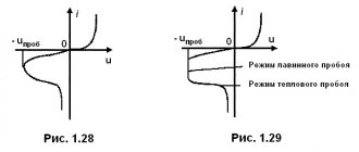
Breakdown of pn junction
Such breakdowns occur in situations where the reverse electric current begins to suddenly and sharply increase, this happens due to the fact that the voltage of the corresponding type reaches unacceptable high values.
There are usually several types:
- Thermal breakdowns , which are caused by a sharp increase in temperature and subsequent overheating.
- Electrical breakdowns that occur under the influence of current on a junction.
The graph of the current-voltage characteristic allows you to visually study these processes and the difference between them.
Electrical breakdown
The consequences caused by electrical breakdowns are not irreversible, since they do not destroy the crystal itself. Therefore, with a gradual decrease in voltage, it is possible to restore all the properties and operating parameters of the diode.
At the same time, breakdowns of this type are divided into two types:
- Tunneling breakdowns occur when high voltage passes through narrow junctions, which allows individual electrons to escape through it. They usually occur if semiconductor molecules contain a large number of different impurities. During such a breakdown, the reverse current begins to increase sharply and rapidly, and the corresponding voltage is at a low level.
- Avalanche types of breakdowns are possible due to the influence of strong fields that can accelerate charge carriers to the maximum level, due to which they knock out a number of valence electrons from atoms, which then fly into the conductive region. This phenomenon is avalanche-like in nature, which is why this type of breakdown received its name.
Disadvantages of a Darlington pair
- Low switching speed
- Bandwidth is limited
- At certain frequencies, this configuration introduces a phase shift in the negative feedback loop.
- The required base-emitter voltage is high and twice that of a standard transistor.
- High power dissipation due to high saturation voltage.
- The total leakage current is high because the leakage current of the first transistor is amplified by the next transistor. This is why three or more Darlington steps are not possible.
Hence, the Darlington pair is very useful in most applications as it provides high current gain at low base currents.
Although this has some limitations, these pairs are widely used in applications where high frequency response is not required but high levels of current gain are required. In case of audio power amplifier circuits, this configuration provides better power output.