In the event of an electrical breakdown, all secondary voltages in the power supply are absent. In the event of a leak, the computer power supply fan may “twitch” and output voltage pulsations may appear at the output and periodically disappear. That is, the protection module periodically fires, but complete blocking does not occur. Schottky diodes are 100% burned out if the radiator on which they are attached is very warm or has a strong burnt smell from them.
On circuit diagrams they are designated almost like a diode, see the figure above, but with slight graphical differences; in addition, dual Schottky diodes are quite common.
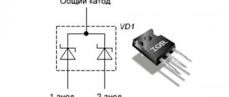
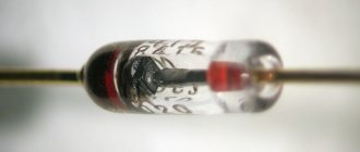
A dual Schottky diode is two separate elements assembled in one common housing and the terminals of the cathodes or anodes of these components are combined. Therefore, a dual diode, usually three terminals. In switching and computer power supplies you can often see dual Schottky diodes with a common cathode.
Since both diodes are placed in a single housing and assembled using the same technological process, their technical parameters are almost identical. With such placement in one case, during operation they will be in the same temperature regime, and this is one of the main factors in increasing the reliability of the device as a whole.
- Maximum constant reverse voltage;
- Maximum pulse reverse voltage;
- Maximum (average) forward current;
- Maximum pulse forward current;
- Constant forward voltage across the diode at a given forward current through it;
- Diode reverse current at maximum reverse voltage;
- Maximum operating frequency of the diode;
- Reverse recovery time;
- Total diode capacity.
In the late 30s of the 20th century, German physicist Walter Schottky discovered that an external electric field forces free electrons to leave the conduction band and literally leave the solid body. This quantum dependence was subsequently named after its discoverer and is now known as the Schottky effect.
Despite the fact that the discovery of the German scientist belongs to the field of theoretical physics, it finds application in practical radio engineering and underlies the functionality of such radio components as Schottky diodes. Their difference from conventional electric valves is the absence of a classic semiconductor pn junction. Its role is played by the contact between the semiconductor and the metal.
Metal and semiconductor: contact features.
In the contact region of semiconductor and metal materials, the Schottky effect leads to the formation of a layer in the semiconductor that is highly depleted of electrons. It has the valve properties inherent in a semiconductor pn junction. This zone is a barrier to charge carriers, which is why these radio components are often called Schottky barrier diodes.
The elements differ from conventional semiconductor valves in the following qualities:
- reduced voltage drop at forward bias;
- insignificant own capacity;
- low reverse current;
- low permissible reverse voltage.
With forward bias, the potential difference across the Schottky diode does not exceed 0.5 V, while on a conventional rectifier valve the voltage drop is about 2-3 V. This is explained by the low resistance of the transition section between the semiconductor and the metal.
Low voltage diodes.
The peculiarity of Schottky diodes is that they are low voltage. If the applied potential difference exceeds a certain permissible level, then, in accordance with quantum laws, a breakdown occurs, which in a conventional semiconductor radio component can be tunneling, avalanche or thermal. After the first two, the diode is restored and continues to work properly. Thermal breakdown means fatal failure.
In diodes with a Schottky barrier, breakdown is always only thermal. This is a feature of the metal-semiconductor junction. If the reverse bias is large, the element fails and needs to be replaced. This, by the way, explains the strong sensitivity of Schottky diodes to static electricity - when installing them and servicing radio equipment with these elements, it is necessary to ground protective clothing and tools.
However, the sensitivity of these radio components is not always their disadvantage. For example, due to this characteristic, Schottky barrier diodes are used in particularly sensitive local oscillators, which gain the ability to process radio signals of very low power.
Main parameters.
- Maximum constant reverse voltage;
- Maximum pulse reverse voltage;
- Maximum (average) forward current;
- Maximum pulse forward current;
- Constant forward voltage across the diode at a given forward current through it;
- Diode reverse current at maximum reverse voltage;
- Maximum operating frequency of the diode;
- Reverse recovery time;
- Total diode capacity.
Production of Schottky diodes.
Standard materials are used as semiconductor components - silicon, germanium and gallium arsenide. In the process of manufacturing radio components, metals such as gold, silver, palladium, and tungsten are sprayed onto them. It is these elements of the periodic table that provide a sufficiently high potential barrier that determines the functionality of Schottky diodes.
Germanium radio components show high resistance to temperature changes, so this material is more often used than silicon and gallium arsenide in the production of diodes for high-power power supply circuits. But silicon and gallium elements demonstrate better frequency parameters.
So the Schottky barrier is a transition between a metal and a semiconductor. In a conventional diode, we use a junction between p-type and n-type semiconductors, but here it’s a completely different story - metal + semiconductor.
Welcome everyone to the MicroTechnics website again! Today we will continue the “Fundamentals of Electronics” course, and the hero of the article will be another electronic component, namely the Schottky diode . In recent articles, we looked at the operating principle and application of conventional diodes and zener diodes:
And now the time has come for the Schottky diode!
The main distinguishing feature of this element is the low voltage drop when connected directly (relative to a conventional rectifier diode). Let's figure out what this reduced decline is connected with in this case.
The “heart” of a Schottky diode is not the pn junction, which is formed when two semiconductors with different types of conductivity come into contact, but the so-called Schottky barrier . Both the element and the barrier are named after the German physicist Walter Schottky, who studied these processes and phenomena in the 1930s.
So the Schottky barrier is a transition between a metal and a semiconductor. In a conventional diode, we use a junction between p-type and n-type semiconductors, but here it’s a completely different story - metal + semiconductor.
For the Schottky barrier to work, it is necessary that the work functions of the metal and semiconductor used be different. And the work function , in turn, is the energy that must be imparted to an electron to remove it from a solid. Let us consider the case when a barrier is formed by contact between a metal and an n-type semiconductor. Moreover, the work function of electrons from the semiconductor is less than the work function of the metal:
Here it is important for us to note that since phi_ > phi_, then, on the contrary, j_. As a result, upon contact between the metal and the semiconductor, charges will accumulate in the boundary region:
In other words, due to the fact that the work function of a semiconductor is less, it is easier for electrons to move from it to the metal than vice versa, in the opposite direction. But as for the pn junction, this process will not proceed indefinitely. These charges will create an additional electric field in the boundary region, and, as a result, under the influence of this field, thermionic emission currents will be equalized.
As you can see, in general, the processes occurring in the Schottky barrier are essentially very similar to what happens in a pn junction when two semiconductors come into contact. When an external voltage is connected, an additional field appears, which shifts the balance of currents in the boundary region.
As you remember, when forward biased in a conventional diode, minority charge carriers accumulate in the semiconductor regions - holes in the n-region and electrons in the p-region:
So, at the moment the diode transitions to the closed state (when reverse bias is applied), minority carriers begin to move towards each other, which leads to the appearance of a short-term reverse current pulse. For Schottky diodes, this negative and undesirable effect is virtually eliminated!
So, let's summarize everything that we have considered and build the current-voltage characteristic of a Schottky diode and a conventional rectifier diode:
Now let’s summarize the pros and cons of these elements:
Now let's do some practical experiments. Let's test two similar circuits for working with high-frequency signals. Only in one circuit we use a Schottky diode , and in the other a regular rectifier diode and compare the oscillograms of the output signals.
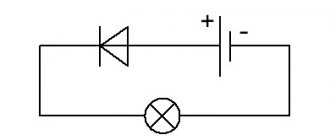
On circuit diagrams, a Schottky diode is designated as follows:
We will conduct tests on a simple half-wave rectifier circuit:
For the experiment, I took Schottky diode and rectifier diode . Let's try to apply a sinusoid with a frequency of 1 KHz to the input:
The first channel (yellow) is the signal at the input. The second channel (red) is the signal at the output of the circuit with a Schottky diode. The third channel (blue) is the signal at the output of the circuit with a conventional diode.
The result is quite expected. Diodes only allow current to pass in one direction, so the lower half-cycle of the input signal is cut off. So far, to be honest, there is no difference. We increase the frequency of the input signal to 100 KHz:
The first channel (yellow) is the signal at the input. The second channel (red) is the signal at the output of the circuit with a Schottky diode. The third channel (blue) is the signal at the output of the circuit with a conventional diode.
And here we already see that a conventional diode simply ceases to cope with such a signal. When the diode switches (from open to closed state), an unwanted reverse current pulse occurs (exactly as we discussed a little earlier).
So, we looked at the device, main characteristics and operating principle of the Schottky diode . Let's end today's article with this, thank you all very much for your time and see you in new articles!
For dual valves, the outputs of the cathodes or anodes are combined. It follows that such a product has three ends. Common cathode assemblies, for example, work where switching power supplies are required. Schottky diodes with a common anode are used much less frequently.
What is a Schottky diode
It differs from a conventional diode element in its small voltage drop. In addition to the semiconductor, it contains metal. The name is in honor of the German physicist Walter Schottky, who discovered the so-called Schottky effect.
On a note!
The metal used for a Schottky zener diode can be tungsten carbide, silicon carbide, palladium, platinum, gold, gallium arsenide and others.
Design
The Schottky diode differs from ordinary diodes in its design, which uses a metal-semiconductor rather than a pn junction. It is clear that the properties here are different, which means the characteristics should also be different.
Indeed, a semiconductor metal has the following parameters:
- The leakage current is of great importance,
- Low voltage drop across the junction when connected directly,
- Restores charge very quickly, as it has a low value.
The Schottky diode is made from materials such as gallium arsenide, silicon, and much less commonly, but can also be used, germanium. The choice of material depends on the properties that need to be obtained, however, in any case, the maximum reverse voltage for which these semiconductors can be manufactured is not higher than 1200 volts - these are the highest voltage rectifiers. In practice, they are much more often used at lower voltages - 3, 5, 10 volts.
This means a dual element: two diodes in one housing with a common anode or cathode, so the element has three terminals. Power supplies use such designs with a common cathode; they are convenient to use in rectifier circuits. Often the diagrams show the markings of a regular diode, but the description indicates that this is a Schottky diode, so you need to be careful.
Diode assemblies with a Schottky barrier are available in three types:
Type 1 – with a common cathode,
Type 2 – with a common anode,
Type 3 – according to the doubling scheme.
This connection helps to increase the reliability of the element: after all, being in the same housing, they have the same temperature regime, which is important if powerful rectifiers are needed, for example, 10 amperes.
But there are also disadvantages. The thing is that the low voltage drop (0.2–0.4 V) of such diodes appears at low voltages, usually 50–60 volts. At higher values they behave like regular diodes. But in terms of current, this circuit shows very good results, because it is often necessary - especially in power circuits and power modules - for the operating current of semiconductors to be at least 10A.
Another major disadvantage: for these devices, the reverse current cannot be exceeded even for an instant. They immediately fail, while silicon diodes, if their temperature has not been exceeded, restore their properties.
But there are still more positive things. In addition to the low voltage drop, the Schottky diode has a low junction capacitance value. As you know: lower capacity - higher frequency. Such a diode has found application in switching power supplies, rectifiers and other circuits with frequencies of several hundred kilohertz.
Current-voltage characteristic of the LED (volt-ampere characteristic)
The current-voltage characteristic of such a diode has an asymmetrical appearance. When a forward voltage is applied, it is clear that the current increases exponentially, and when reverse voltage is applied, the current does not depend on the voltage.
All this can be explained if you know that the operating principle of this semiconductor is based on the movement of the main carriers - electrons. For the same reason, these devices are so fast: they do not have recombination processes characteristic of devices with pn junctions. All devices with a barrier structure are characterized by asymmetry of the current-voltage characteristics, because it is the number of electric charge carriers that determines the dependence of current on voltage.
Testing and interchangeability
Schottky rectifiers can be tested in the same way as conventional semiconductors, since they have similar characteristics. You need to ring it in both directions with a multimeter - it should show itself in the same way as a regular diode: anode-cathode, and there should be no leaks. If it shows even a slight resistance - 2-10 kilo-ohms, this is already a reason for suspicion.
Checking a Schottky diode with a multimeter
A diode with a common anode or cathode can be tested like two ordinary semiconductors connected together. For example, if the anode is common, then it will be one leg out of three. We place one tester probe on the anode, the other legs are different diodes, and another probe is placed on them.
Can it be replaced with another type? In some cases, Schottky diodes are replaced with ordinary germanium diodes. For example, D305 at a current of 10 amperes gave a drop of only 0.3 volts, and at currents of 2–3 amperes they can generally be installed without radiators. But the main purpose of the Schottky installation is not a small drop, but a low capacity, so replacement will not always be possible.
As we see, electronics does not stand still, and further applications of high-speed devices will only increase, making it possible to develop new, more complex systems.
Schottky diodes, or more precisely Schottky barrier diodes, are semiconductor devices made on the basis of a metal-semiconductor contact, while conventional diodes use a semiconductor pn junction.
The Schottky diode owes its name and appearance in electronics to the German physicist and inventor Walter Schottky, who in 1938, while studying the newly discovered barrier effect, confirmed the previously put forward theory, according to which although the emission of electrons from a metal is prevented by a potential barrier, but as the applied external electric field, this barrier will decrease. Walter Schottky discovered this effect, which was then called the Schottky effect, in honor of the scientist.
Examining the contact between a metal and a semiconductor, one can see that if near the surface of the semiconductor there is a region depleted of major charge carriers, then in the region of contact of this semiconductor with the metal on the side of the semiconductor, a region of space charge of ionized acceptors and donors is formed, and a blocking contact is realized - the same Schottky barrier . Under what conditions does this barrier arise? Thermionic emission current from the surface of a solid body is determined by the Richardson equation:
Let us create conditions when, when a semiconductor, for example n-type, comes into contact with a metal, the thermodynamic work function of electrons from the metal would be greater than the thermodynamic work function of electrons from the semiconductor. Under such conditions, in accordance with the Richardson equation, the thermionic emission current from the surface of the semiconductor will be greater than the thermionic emission current from the metal surface:
At the initial moment of time, upon contact of the named materials, the current from the semiconductor to the metal will exceed the reverse current (from the metal to the semiconductor), as a result of which space charges will begin to accumulate in the near-surface regions of both the semiconductor and the metal - positive in the semiconductor and negative in the semiconductor. metal An electric field formed by these charges will arise in the contact area, and the energy zones will bend.
Under the influence of the field, the thermodynamic work function for the semiconductor will increase, and the increase will occur until the thermodynamic work functions and the corresponding thermionic emission currents in relation to the surface are equalized in the contact region.
How does a Schottky diode work?
The element structure includes several parts:
- epitaxial layer;
- substrate;
- security ring;
- metal film;
- barrier;
- external contact.
The base is usually made of silicon or gallium arsenide, but if the circuit needs to be highly resistant to temperature changes, germanium is used. The materials used for sputtering are palladium, silver, platinum, tungsten, aluminum or gold. It is noteworthy that the back side of the semiconductor is more heavily doped. The level of alloying and type of metal affect the rectification characteristics.
The operating principle is based on the characteristics of the barrier. In the semiconductor, in the contact region, a layer is formed that is significantly depleted of electrons, but has valve properties. Thus, a barrier for charge carriers appears.
Depending on the power, there are several types of Schottky diodes:
- small;
- average;
- high.
Based on the design features, there are types for surface or volumetric mounting, as well as modules and rectifier analogues. When choosing rectifier components, you should pay attention to the current and voltage indicators, as well as the material of construction and mounting method. There are also 3 variations of diode assemblies: models with a common anode, elements with doubling and three leads, as well as varieties that have a lead from a common cathode. For all types, there is a limit on the permissible reverse voltage of 1200 volts.
How a Schottky diode is marked and indicated in diagrams
Often, a Schottky diode will be labeled as a regular diode on a schematic, and additional information about the type of component will be included in the specification sheet.
As a rule, the marking of Schottky diodes is a set of symbols printed on the product body in accordance with international standards. Depending on the country of origin, labeling may vary. In any case, you can decipher the code using radio engineering reference books.
If necessary, you can replace the standard diode with a similar device with a barrier - the main thing is that the current and voltage parameters match. But it is strictly not recommended to install a classic product instead of a barrier analogue, since it will quickly fail due to overheating. Experienced radio technicians can select an element with a power reserve by analyzing the entire circuit.
Types of Schottky diodes
All semiconductor elements operating on the Schottky barrier principle are divided by power into:
- high;
- average;
- low power.
Dual diode
The figure shows a dual element, which is essentially two elements. They are located in a single housing, connected as a whole by a cathode or anode. In this case, most often there are three diode terminals. With identical parameters of the elements assembled in this way, the reliability of the entire device is ensured, primarily due to a uniform temperature.
Symbol and characteristics
In the diagram, the Schottky diode has a special designation. The difference from the usual one is that the crossbar of the triangle has curved edges. Not one, like a zener diode, but both. And these edges are bent in different directions. The figure shows the designation according to GOST.
Schottky diode in the diagram: symbol
We have already talked about the characteristics. These are three main parameters:
- Voltage drop during forward transition. For Schottky diodes it is lower than for conventional silicon diodes. With a reverse breakdown power of up to 100 V, it will be on the order of 0.2-0.4 V (for silicon on average 0.6-0.7 V).
- Breakdown voltage. The usual value is up to 200 V, but there are also products with voltages of more than 1000 volts.
Parameters of the popular series of Schottky diodes 1N58**- Reverse current. Under normal conditions (up to 20 °C) it is not too high - about 0.05 mA, but as the temperature rises it increases sharply.
The given parameters are average. There is a fairly serious range and for each case you can select the necessary characteristics for each of the points. Sometimes such a parameter as switching speed (performance) is also important.
Notes on tables
1. The values of forward voltage drops are given for a junction temperature of 25°C, maximum values (typical - 50...80 mV less), indicating the current in amperes. The TKN of forward voltages at low currents is always negative, but at high currents it can often become positive, especially for diodes with UR > 40...60 V.
2. The values of reverse currents (IR) are given as standard, in milliamps.
3. IFSM - the value of a single shock current in the form of one half-cycle of frequency 50 Hz, amplitude value.
4. Diode capacitance is a nonlinear quantity, given here in picofarads at a reverse voltage of 4 V. It allows you to estimate the order of dynamic switching losses (more precisely, switching charge) in most application circuits.
5. “VAC” is a conditional parameter. Qualitatively describes the behavior of the diode at high currents. “R” is resistive in nature, “R+” is resistive with a noticeable positive TKN, “D” is “diode” (the influence of the parallel pn junction diode is strongly pronounced), “D-” is diode with a pronounced negative TKN, “DеR” is something average.
6. Dual diodes are marked with an asterisk (“*”).
Main characteristics of diodes
First, let's remember what a regular diode is and how it works. This is a semiconductor device that consists of two zones. Under certain conditions, electrons move through this transition.
Diode design and designation
The main property of the element is that it allows current to pass in one direction and not in the other. Schottky diodes have the same characteristics as conventional ones. Let’s focus on some in more detail. These are voltage drop, reverse current, reverse voltage, frequency.
Reference verification model for calculating a semiconductor Schottky diode
Schottky diodes are one of the oldest semiconductor elements still used in modern devices, including computers and radar. To be completely confident that a Schottky diode will operate correctly, engineers need to consider factors such as current density and potential barrier height when designing. The reference model below confirms that COMSOL Multiphysics® with the Semiconductor Extension is well suited to solve these problems.
A Brief History of the Schottky Diode
The operating principle of a Schottky diode was first demonstrated in 1874 by Karl Ferdinand Braun. By combining a metal wire and a galenic crystal (which acted as a semiconductor), Brown created a point-contact diode that converted alternating current into direct current (i.e., rectified the current). This device was one of the first examples and concepts of a semiconductor diode, but Brown's work did not attract much attention because... at that time there were no practical applications for it.
Schottky diode is different from conventional silicon diodes
Schottky diodes are made from silicon (Si), gallium arsenide (GaAs), and rarely germanium (Ge). The metal in connection with the semiconductor determines many of the parameters of the diode. This metal may be gold (Au), rallyadium (Pd), platinum (Pt), tungsten (W) which is deposited on semiconductors.
And just like a regular diode, the semiconductor-metal connection has one-way conductivity with a number of positive as well as negative qualities.
Current-voltage characteristic of a Schottky diode
The current-voltage characteristic of a Schottky diode differs from a conventional semiconductor diode by being more nonlinear.
What are the benefits of using a metal-semiconductor connection? Two positive points:
- A very small voltage drop across the direct junction is 0.2-0.4 V. For a silicon diode, the “average” value of this parameter is 0.7 V. However, only devices with a low breakdown voltage - up to 100 V have a low voltage drop. For more powerful ones, the drop is only slightly lower than for silicon ones.
- High performance. That is, he quickly changes his state. The transition from an open state to a closed state and back occurs in a very short period of time and is determined only by the barrier capacitance. They are used in switching systems where response speed is important.
What is a Schottky diode and how is it indicated in the diagram
They also have disadvantages. As the temperature rises, their reverse current increases significantly.
The second drawback is that if the maximum permissible reverse voltage is exceeded, an irreversible breakdown occurs. That is, the device fails. There is one more disadvantage - the low forward voltage drop is only found in Schottky diodes with a low breakdown voltage (up to hundreds of volts). Higher voltage variants have losses comparable to silicon ones.
Content
- 1 Construction
- 2 Reverse recovery time
- 3 Limitations
- 4 Silicon carbide Schottky diode
- 5 Applications 5.1 Voltage clamping
- 5.2 Reverse current and discharge protection
- 5.3 Switching power supplies
- 5.4 Sample and hold circuits
- 5.5 Charge control
Application in electronics
Properties such as speed and low voltage drop allow the use of Schottky diodes in high-frequency circuits. For example, in high-frequency power rectifiers (up to hundreds of kilohertz), where they work as high-frequency rectifiers. They are also used in sound amplifiers, since compared to conventional diodes they produce a lower level of interference.
If you look at the power supply board, you will definitely see a Schottky diode
Another application is as an integral part of more complex semiconductor devices. For example, MOS transistors, diode assemblies and power diodes with a built-in Schottky diode have better characteristics.
The scope of application of the products is wide, but they are most often used in computer power supplies. And also in circuits for modulating light in radiation receivers and solar batteries.
Scope of application
The Schottky diode can be included in any battery.
It is included in the solar battery device. Solar panels, which have been successfully operating in outer space for a long time, are assembled precisely on the basis of Schottky barrier junctions. Such solar systems are installed on spacecraft (satellites and telescopes that operate in harsh conditions of airless space).
The device is indispensable when operating computers, household appliances, radios, and power supplies. When used correctly, a Schottky diode increases the performance of any device and prevents current loss. It is capable of receiving alpha, beta and gamma radiation. That is why it is indispensable in space conditions.
Using such a device, it is possible to connect diodes in parallel, using them as dual rectifiers. In this way, you can combine two parallel power supplies. One package includes two semiconductors, and the ends of the positive and negative charges are connected to each other. There are also simpler circuits where Schottky diodes are very small. This is typical for very small parts in electronics.
The Schottky diode is an indispensable element in many electronic devices. The main thing is to understand the specifics of its work and use it correctly.
Differences from a conventional diode
This component passes electric current in one direction and does not pass it in the other, like other classic diodes, but provides high speed and low voltage drop during transition.
The most important feature of the Schottky diode is that instead of the usual electron-hole junction, the principle of contact between metal and various semiconductor materials is used, which has a positive effect on increasing the operating frequency. Diffuse capacitance and the recombination process do not appear in the contact region, since there are no minority charge carriers in the so-called transition zone. The intrinsic capacity of this layer tends to 0.
Thus, these products are microwave diodes for various purposes:
- pulsed;
- avalanche-flight;
- mixing;
- detector;
- multiplying;
- parametric.
Another feature is that most Schottky diodes are low voltage and static sensitive models. However, it is wrong to perceive this as a categorical disadvantage, since this makes it possible to use these tools for processing low-power radio signals.
Finally, such products are more stable when applying electric current than other analogues, since crystal formations (silicon substrate) are embedded in their body.
Advantages and disadvantages
The diodes described above have some advantages, which are as follows:
- the electric current is perfectly contained in the circuit;
- the small capacity of the Schottky barrier increases the service life of the product;
- low voltage drop;
- speed in an electrical circuit.
What is a diode
The most significant drawback of the component is the huge reverse current, which even if this indicator jumps by several units leads to failure of the diode.
Note! When operating a Schottky electric element in circuits with a powerful electric current under unfavorable heat exchange conditions, a thermal breakdown occurs.
Schottky diode reverse voltage
So, as you remember, a diode allows electric current to pass in only one direction, and in the other direction it blocks the passage of electric current to some critical value, called the diode reverse voltage.
This value can be found in the datasheet
diode reverse voltage
It is different for each brand of diode
If this value is exceeded, a breakdown will occur and the diode will fail.
What it is
This is a semiconductor diode with a minimal voltage drop during direct switching. It has two main components: the semiconductor itself and the metal. As is known, the permissible level of reverse voltage in any industrial electronic devices is 250 V. This U finds practical application in any low-voltage circuit, preventing the reverse flow of current.
The structure of the device itself is simple and looks like this:
- semiconductor;
- glass passivation;
- metal;
- protective ring.
When electric current passes through a circuit, positive and negative charges accumulate around the entire perimeter of the device, including the protective ring. Particle accumulation occurs in various diode elements. This ensures the emergence of an electric field with the subsequent release of a certain amount of heat.
Miniaturization
With the development of microelectronics, special microcircuits and single-chip microprocessors began to be widely used. All this does not exclude the use of hanging elements. However, if radioelements of conventional sizes are used for this purpose, this will negate the whole idea of miniaturization as a whole. Therefore, open-frame elements were developed - SMD components, which are 10 or more times smaller than conventional parts. The current-voltage characteristics of such components are no different from the current-voltage characteristics of conventional devices, and their reduced dimensions make it possible to use such spare parts in various microassemblies.
SMD components come in several sizes. SMD size 1206 is suitable for manual soldering. They have a size of 3.2 by 1.6 mm, which allows you to solder them yourself. Other SMD elements are more miniature, assembled at the factory with special equipment, and it is impossible to solder them yourself at home.
The operating principle of an smd component is also no different from its large counterpart, and if, for example, we consider the current-voltage characteristic of a diode, then it will be equally suitable for semiconductors of any size. The current range is from 1 to 10 amperes. The markings on the case often consist of a digital code, the decoding of which is given in special tables. They can be tested for suitability using a tester, just like their larger counterparts.
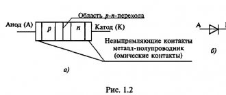
Metal and semiconductor: contact features
In the contact region of semiconductor and metal materials, the Schottky effect leads to the formation of a layer in the semiconductor that is highly depleted of electrons. It has the valve properties inherent in a semiconductor pn junction. This zone is a barrier to charge carriers, which is why these radio components are often called Schottky barrier diodes.
The elements differ from conventional semiconductor valves in the following qualities:
- reduced voltage drop at forward bias;
- insignificant own capacity;
- low reverse current;
- low permissible reverse voltage.
With forward bias, the potential difference across the Schottky diode does not exceed 0.5 V, while on a conventional rectifier valve the voltage drop is about 2-3 V. This is explained by the low resistance of the transition section between the semiconductor and the metal. The table below shows the characteristics of Schottky diodes.
The good frequency characteristics of Schottky diodes are due to the absence of minority charge carriers in the transition zone. Because of this, the processes of diffusion and recombination of holes and electrons that are usual for a purely semiconductor pn junction do not occur in the contact region.
Consequently, the intrinsic capacitance of this layer tends to zero. This property makes Schottky barrier diodes preferable for use in high- and ultra-high-frequency circuits, as well as equipment with pulsed operating modes - all kinds of digital devices, electronics control systems and switching power supplies.
27. Vertical structure of the Schottky transistor.
The most widely used transistors are those that have a vertical structure, in which all leads from the transistor areas are located in the same plane on the surface of the substrate. This structure is called planar.
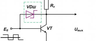
To speed up the process of accumulation and resorption of minority charge carriers, it is advisable to limit their accumulation. This can be achieved by shunting the collector junction of the transistor with a Schottky diode, i.e., a diode with a rectifying electrical junction between the metal and the semiconductor. The structure of such an integrated transistor is shown in Fig. 7.5.
Rice. 7.5. Structure of a transistor with a Schottky diode
Sometimes it is difficult to graphically designate this element on circuit diagrams; it is drawn like a regular diode, and the type is additionally indicated in the specification.
Voltage drop across a Schottky diode
If you apply direct current to the diode, then the voltage will “settle” on the diode. This voltage drop is called the forward voltage drop of the diode. In datasheets it is designated as Vf, that is, Voltage drop.
forward voltage drop across the diode
If you pass direct current through such a diode, then the power that will be dissipated by it will be determined by the formula:
Where
P – power, W
Vf – forward voltage drop across the diode, V
I – current through the diode, A
Therefore, one of the main advantages of a Schottky diode is that its forward voltage drop is much lower than that of a simple diode. Consequently, it will dissipate less heat, or in simple terms, heat up less.
Let's look at one example. Let's take a 1N4007 diode. Its forward voltage drop is 0.83 Volts, which is typical for a simple semiconductor diode.
voltage drop across the diode in direct connection
At the moment, a current of 0.5 A is passing through it. Let's calculate its power dissipation at the moment. P=0.83 x 0.5 = 0.415 W.
If we look at this case through a thermal imager, we can see that its body temperature was 54.4 degrees Celsius.
Now let's do the same experiment with a 1N5817 Schottky diode. As you can see, its forward voltage drop was approximately 0.35V.
voltage drop across the Schottky diode when connected directly
When a current of 0.5 A passes through a Schottky diode, we get a power dissipation of P = 0.5 x 0.35 = 0.175 W. At the same time, the thermal imager will show us that the body temperature will already be 38.2 degrees.
Consequently, Schottky is much more efficient than a simple semiconductor diode in terms of passing forward current through itself, since it has a lower voltage drop, and therefore dissipates less heat into the surrounding space and heats up less.
The forward voltage drop can also be viewed in datasheets. For example, the forward voltage drop across a 1N5817 Schottky diode can be found from a graph of forward current versus voltage drop across a Schottky diode
graph of forward current versus voltage
In our case, if we follow the graph-analytical method, we just get a value of 0.35 V
Designation
SS14 Schottky diode in DO-214 AC (SMA) package (surface mount version 1N5819)[10]
Commonly found Schottky diodes include 1N58xx series rectifiers such as 1N581x (1) and 1N582x (3A) through-pieces,[6][11 ] and surface mount parts SS1x (1 A) and SS3x (3 A).[10][12] Schottky rectifiers are available in a variety of surface mount housing styles.[13][14]
Small signal Schottky diodes such as 1N5711,[7] 1N6263, g.[15] 1SS106,[16] 1SS108,[17] and BAT41–43, 45–49 series[18] are widely used in high frequency applications as detectors, mixers and nonlinear elements and have replaced germanium diodes.[19] They are also suitable for electrostatic discharge (ESD) protection of sensitive devices such as III-V semiconductor devices, laser diodes and, to a lesser extent, bare-line CMOS circuitry.
Metal-to-semiconductor Schottky junctions are introduced in the successors to the 7400 TTL family of logic devices, the 74S, 74LS, and 74ALS, where they are used as Baker clamps in parallel with the collector-to-base junctions of bipolar transistors to prevent them from saturating, thereby significantly reducing turn-off delays.
Schottky diode in RF circuits
Schottky diodes also have fast switching speed. This means we can use them in high frequency (RF) circuits.
So, let's take a frequency generator and set the sine frequency to 60 Hz
Let's take a 1N4007 diode and a 1N5817 Schottky diode. Let's connect them using a simple half-wave rectifier circuit
and we will take evidence from them
As you can see, both of them do an excellent job of rectifying the signal at a frequency of 60 Hz.
But what happens if we increase the frequency to 300 kHz?
Wow! The Schottky diode more or less copes with its task, which cannot be said about a simple 1N4007 diode. A simple diode cannot cope with its task of not allowing reverse current to pass through, so we see a negative surge on the oscillogram
From this we can conclude: Schottky diodes are recommended for use in RF circuits.
Reverse recovery time
The most important difference between a n-p diode and a Schottky diode is the reverse recovery time (trr), when the diode switches from a conducting state to a non-conducting state. In a p−n diode, the reverse recovery time can range from a few microseconds to less than 100 ns for fast diodes, and it is mainly limited by the diffusion capacitance caused by minority carriers accumulated in the diffusion region during the conducting state.[3] Schottky diodes are significantly faster because they are unipolar devices and their speed is limited only by the junction capacitance. Switching time is ~ 100 for small-signal diodes and up to tens of nanoseconds for special high-power high-capacity diodes. When switching a p–n junction, a reverse recovery current also arises, which in power semiconductors increases EMI noise. Schottky diodes switch almost instantly with little capacitive load, which is not a concern.
This "instant" switching does not always happen. Particularly in higher voltage Schottky devices, the guard ring structure required to control the breakdown field geometry produces a parasitic pn diode with the usual recovery time attributes. As long as this protection ring diode is not forward biased, it only adds capacitance. However, if the Schottky junction is driven hard enough, the forward voltage will eventually drive both diodes forward and the actual trr will be greatly affected.
It is often said that the Schottky diode is a "primary operator" semiconductor device. This means that if the semiconductor body is n-type doped, only n-type carriers (mobile electrons) play a significant role in the normal operation of the device. Most carriers are quickly introduced into the conduction band of the metal contact on the other side of the diode to become free-moving electrons. Therefore, there is no slow random recombination of n- and p-type carriers, so this diode can stop conducting faster than a conventional p−n rectifier. diode. This property, in turn, allows the device footprint to be reduced, which also contributes to faster transition times. This is another reason why Schottky diodes are useful in pulsed mode. Power Converters: The diode's high speed means that the circuit can operate at frequencies ranging from 200 kHz to 2 MHz, allowing the use of small inductors and capacitors with greater efficiency than would be possible with other types of diodes. Small area Schottky diodes are the heart of RF detectors and mixers, often operating at frequencies up to 50 GHz.
Reverse leakage current
But since Schottky diodes are so cool, why not use them everywhere? Why do we still use simple diodes?
If we connect the diode in the opposite direction, it will block the passage of electric current. This is true, but not entirely. Very little current will still flow through the diode. In some cases this is not taken into account. This small current is called reverse leakage current. In English it sounds like reverse leakage current.
It is very small, but it exists.
Let's do a simple experiment. Let's take a laboratory power supply, set it to 19 V and apply this voltage to the diode in the opposite direction
We measure the leakage current
diode reverse leakage current
As you can see, its value is 0.1 µA.
Let's now repeat the same experiment with a Schottky diode
Schottky diode reverse leakage current
Wow, almost 20 µA already! Well, yes, in some cases these are mere pennies and can be ignored. But there are circuits where such a small current is still unacceptable. For example, in peak detector circuits
peak detector circuit
In this case, these 20 µA will be quite significant.
But there is also another stumbling block. As the temperature increases, the reverse leakage current increases significantly!
dependence of the reverse leakage current on the body temperature of the Schottky diode
Therefore, you cannot use Schottky everywhere in the circuits.
But that's not all. The reverse voltage for Schottky diodes is several times less than for simple rectifier diodes. This can also be seen from the datasheet. If the reverse voltage is 1000V for the 1N4007 diode
Then for a 1N5817 Schottky diode this reverse voltage will already be only 20 V
Therefore, if this voltage exceeds the value described in the datasheet, we will end up with:
Restrictions
The most obvious limitations of Schottky diodes are their relatively low reverse voltage ratings and relatively high reverse voltage ratings. reverse leakage current. For silicon metal Schottky diodes, the reverse voltage is typically 50V or less. Some higher voltage designs are available (200V is considered high reverse voltage). Reverse leakage current, because it increases with temperature, leads to thermal instability problem. This often limits the useful reverse voltage to well below the actual nominal value.
Although higher reverse voltages are achievable, they will produce higher forward voltages comparable to other types of standard diodes. Such Schottky diodes would have no advantage. [4] if high switching speed is not required.
Low voltage diodes
The peculiarity of Schottky diodes is that they are low voltage. If the applied potential difference exceeds a certain permissible level, then, in accordance with quantum laws, a breakdown occurs, which in a conventional semiconductor radio component can be tunneling, avalanche or thermal. After the first two, the diode is restored and continues to work properly. Thermal breakdown means fatal failure.
Schottky diode bridge
However, the sensitivity of these radio components is not always their disadvantage. For example, due to this characteristic, Schottky barrier diodes are used in particularly sensitive local oscillators, which gain the ability to process radio signals of very low power.
Main parameters:
- Maximum constant reverse voltage;
- Maximum pulse reverse voltage;
- Maximum (average) forward current;
- Maximum pulse forward current;
- Constant forward voltage across the diode at a given forward current through it;
- Diode reverse current at maximum reverse voltage;
- Maximum operating frequency of the diode;
- Reverse recovery time;
- Total diode capacity.
In diodes with a Schottky barrier, breakdown is always only thermal. This is a feature of the metal-semiconductor junction. If the reverse bias is large, the element fails and needs to be replaced. This, by the way, explains the strong sensitivity of Schottky diodes to static electricity - when installing them and servicing radio equipment with these elements, it is necessary to ground protective clothing and tools.
Schottky diode on an electrical circuit
Recommendations
- ''Lawton, M.A. (2003). "17. Power semiconductor devices". Electrician's Handbook
. Newnes. pp. 25–27. ISBN 978-0-7506-4637-6. Retrieved 2011-05-16. - Hastings, Alan (2005). The Art of Analog Layout
(2nd ed.). Prentice Hall. ISBN 0-13-146410-8. - Pierre, Robert F. (1996). Fundamentals of Semiconductor Devices
. Addison-Wesley. ISBN 978-0-131-78459-8. - "Introduction to Schottky Rectifiers" (PDF). MicroNotes
. 401. Schottky rectifiers rarely exceed an operating peak reverse voltage of 100 V, since devices moderately above this rated level will produce forward voltages equal to or greater than equivalent pn junction rectifiers. - ^ a b
"Schottky diodes: old ones are good, new ones are better."
Power electronics
. - ^ a b
"1N5817 Passports (PDF)". Datasheetcatalog.com. Retrieved 2013-01-14. - ^ a b
"1N5711 Datasheets (PDF)". Datasheetcatalog.com. Retrieved 2013-01-14. - Jones, David A. and Martin, Ken. Analog Integrated Circuit Design
(1997), Wiley. Page 351. ISBN 0-471-14448-7 - O. D. Couto Jr., J. Puebla, E. A. Chekhovich, I. J. Luxmoore, K. J. Elliott, N. Babazadeh, M. S. Skolnik, A. I. Tartakovsky Charge control in single quantum InP/(Ga, In)P points built into Schottky diodes
(2011), Physical Review B 84, 125301. Doi:10.1103/PhysRevB.84.125301 - ^ a b
"SS14 Passports (PDF)". Datasheetcatalog.com. Retrieved 2013-11-23. - "1N5820 Datasheets (PDF)". Datasheetcatalog.com. Retrieved 2013-11-23.
- "SS34 Passports (PDF)". Datasheetcatalog.com. Retrieved 2013-11-23.
- Bourns Schottky straighteners.
- Vishay Schottky straighteners.
- "1N6263 Passports (PDF)". Datasheetcatalog.com. Retrieved 2013-01-14.
- "1SS106 Data Tables (PDF)". Datasheetcatalog.com. Retrieved 2013-01-14.
- "1SS108 Datasheets (PDF)". Datasheetcatalog.com. Retrieved 2013-01-14.
- "BAT4 Data Tables (PDF)". Datasheetcatalog.com. Retrieved 2013-01-14.
- Vishay small signal Schottky diodes.
- S. Arscott and M. Gaudet "Electrowetting at the liquid metal-semiconductor junction" Appl. Phys. Lett. 103
, 074104 (2013). doi:10.1063/1.4818715 - Advances RKTs S. Arscott "Electrowetting and semiconductors" 4
, 29223 (2014). Doi:10.1039/C4RA04187A
Production of Schottky diodes
Standard materials are used as semiconductor components - silicon, germanium and gallium arsenide. In the process of manufacturing radio components, metals such as gold, silver, palladium, and tungsten are sprayed onto them. It is these elements of the periodic table that provide a sufficiently high potential barrier that determines the functionality of Schottky diodes. Germanium radio components show high resistance to temperature changes, so this material is more often used than silicon and gallium arsenide in the production of diodes for high-power power supply circuits. But silicon and gallium elements demonstrate better frequency parameters.
Advantages and disadvantages
When working with devices that include a Schottky diode, you should consider their positive and negative aspects. If you connect it as an element of an electrical circuit, it will perfectly hold the current, preventing large losses.
In addition, the metal barrier has minimal capacity. This significantly increases the wear resistance and service life of the diode itself. The voltage drop when using it is minimal, and the action occurs very quickly - you just need to make a connection.
However, the large percentage of reverse current is an obvious disadvantage. Since many electrical appliances are highly sensitive, there are often cases when a slight excess of the indicator, just a couple of A, can damage the device for a long time. Also, if you carelessly check the semiconductor voltage, the diode itself may leak.
Operating principle and designation
If a conventional semiconductor diode is based on the properties of a pn junction, then the operating principle of a Schottky diode is based on the properties of a junction at the contact of a metal and a semiconductor. In physics, such a contact is called the “Schottky barrier.” Gallium arsenide (GaAs) is most often used as a semiconductor, and the following metals are mainly used:
- tungsten;
- platinum;
- silver;
- gold;
- palladium.
On radio circuits, the designation of a Schottky diode is similar to the designation of a conventional semiconductor element, but there is a noticeable difference: on the cathode side, where there is a small line perpendicular to the main line, its edges are additionally bent in different directions at a right angle or with a smooth bend.
Sometimes it is difficult to graphically designate this element on circuit diagrams; it is drawn like a regular diode, and the type is additionally indicated in the specification.
When electric current passes through a circuit, positive and negative charges accumulate around the entire perimeter of the device, including the protective ring. Particle accumulation occurs in various diode elements. This ensures the emergence of an electric field with the subsequent release of a certain amount of heat.