I want to say right away that there is no fuss about the zener diode here, and only the necessary information. In order to better understand what a zener diode, zener diode, protective diode, stabistors, stabistor, precision zener diodes are, I strongly recommend reading everything from the category Electronics, Microelectronics, Element base
There is a wide variety of semiconductor devices - Schottky diodes, Gunn diodes, zener diodes, LEDs, photodiodes, tunnel diodes and many more different types and applications.
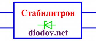
Semiconductor diodes, which are characterized by a weak dependence of voltage on current in the region of electrical breakdown under reverse bias, are called zener diodes.
A zener diode is a semiconductor diode, the voltage on which in the region of electrical breakdown during reverse bias weakly depends on the current in a given range, and which is designed to stabilize the voltage level in the circuit. A zener diode is a radio component that is structurally similar to a diode, but is radically different from it in the nature of its operation. The key element, just as in a conventional semiconductor valve, is the semiconductor pn junction. And the reactions of both elements to the supply of reverse voltage are similar - they both lock. The difference is that the breakdown of the pn-transition zone, which occurs when the reverse bias reaches a certain critical value and disables the diode, is the operating mode for the zener diode.
The starting material is silicon, which provides low reverse currents, a wide temperature range, and a high slope of the current-voltage characteristic in the region of stabilization voltage. The operating principle of zener diodes is based on the use of the property of a pn junction during electrical breakdown to maintain an almost constant voltage value within a certain range of changes in the reverse current. The breakdown mechanism can be tunnel, avalanche or mixed.
The basis of the functionality of the zener diode is that with fairly large changes in the reverse current, the voltage on the element remains practically unchanged. In other words, no matter how significant the reverse bias is, the radio component will maintain a constant level of output potential difference. This stabilized voltage can be used as a reference voltage, which is used in real electronic devices that are critical to the electrical characteristics of the signal.
For a semiconductor zener diode (Fig. 11.4, a), in operating mode the reverse branch of its current-voltage characteristic is used (Fig. 11.4, b), and in the area corresponding to electrical breakdown.
Rice. 11.4. Semiconductor Zener diode:
a - conventional image; b - I-V characteristics of the zener diode
Tunnel and avalanche breakdown
The breakdown of the pn junction, at which zener diodes operate, can be avalanche or tunnel. They are electrical and reversible. That is, when the reverse bias is turned off, the physicochemical properties of the semiconductors are restored, and the diode continues to perform its functions. However, in the case of zener diodes, the conditions for the occurrence of breakdown are created and maintained artificially. Avalanche and tunnel breakdown are based on quantum effects of the same name, observed in the crystal structure of a semiconductor when an electric field is excited. With different natures and mechanisms of these processes, their consequences are the same - electrons acquire energy sufficient to pass through the pn junction. A breakdown occurs and reverse current begins to flow through the diode. It is in this mode that the zener diode operates. However, there is a difference between radio components that use different effects. Zener diodes operating during avalanche breakdown operate with potential differences of over 7 Volts. In elements designed for a stabilization voltage of 3-7 Volts, a tunnel breakdown is provoked. To stabilize lower potential differences, stabistors are used, which we will discuss below.
Classification of zener diodes
Currently, a wide range of zener diodes are produced, but their entire mass is classified according to functional characteristics and design. Depending on the parameters, these radio components are divided into the following classes:
- precision;
- dual-anode;
- fast-acting.
Precision ones are characterized by high voltage stabilization accuracy. The website https://intellect.icu talks about this. Deviations of the stabilized potential difference at the output of such a part do not exceed 0.0001%. The accuracy is highly dependent on the lifetime of the precision zener diode and the temperature of the semiconductor. In this regard, operating standards have been introduced for these radio components, which must be constantly monitored during use of the equipment. A two-node zener diode performs the function of two zener diodes connected back to back. This allows the element to process signals and handle voltages of different polarities with equal efficiency. Such a radio component is manufactured in a single technological cycle, when two opposing pn junctions are grown on one silicon crystal, but, in principle, the role of a two-anode radio component can also be played by two discrete zener diodes mutually connected by cathodes. And finally, zener diodes of the third type - high-speed - are characterized by a reduced barrier capacitance, as a result of which the duration of transient processes occurring in the semiconductor is reduced. These radio components are the best solution for working with pulsed signals. The design feature of these elements is the small width of the pn junction, which is ensured by the use of a special semiconductor doping technology.
Stabistor
The radio components called stabistors, which we discussed above, function a little differently. They perform the same function, that is, they stabilize the output voltage, but are low-voltage. Conventional zener diodes are not capable of operating with small potential differences. At voltages up to 3 Volts, there are no conditions for either avalanche or tunnel breakdown of the pn junction. To stabilize lower voltages, they resort to another solution, namely, using forward bias rather than reverse bias. It has been established that in a heavily doped pn junction, holes and electrons recombine in such a way that, with a significant forward current, the effect of stabilizing the output voltage at a level of 2.5-3 Volts is observed. This determines the key technological difference between zener diodes and stabilizers. The latter are designed to work only in low-voltage radio circuits.
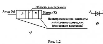
Schottky diode
The Schottky diode does not use a pn junction, but a metal-semiconductor rectifying contact. The symbolic graphic designation of a Schottky diode is shown in Fig. 1.44, b.
Let us turn to the corresponding band diagram (Fig. 1.47), which is useful to compare with the band diagram for a non-rectifying contact.
For an n-type metal-semiconductor rectifying contact, it is characteristic that the contact potential difference φmp = φm - φp is positive: φmp > 0.
Abrahamyan Evgeniy Pavlovich
Associate Professor, Department of Electrical Engineering, St. Petersburg State Polytechnic University
Ask a Question
The energy levels corresponding to the conduction band are more filled in a semiconductor than in a metal. Therefore, after connecting the metal and the semiconductor, some electrons will move from the semiconductor to the metal. This will lead to a decrease in the electron concentration in the n-type semiconductor. A region of the semiconductor will appear that is depleted of free carriers of electricity and has an increased resistivity. Space charges will appear in the transition region and a potential barrier will form, preventing the further transition of electrons from the semiconductor to the metal.
If you connect an external voltage source with a plus to the metal and a minus to an n-type semiconductor, then the potential barrier will decrease and direct current will begin to flow through the junction. With the opposite connection, the potential barrier increases and the current turns out to be very small.
When a Schottky diode operates, there is no injection of minority carriers and the corresponding accumulation and resorption phenomena, therefore Schottky diodes are very fast devices; they can operate at frequencies up to tens of gigahertz (1 GHz = 1 × 10⁹ Hz). A Schottky diode can have a low reverse current and a low forward voltage (at low forward currents) - about 0.5 V, which is less than that of silicon devices. The maximum permissible forward current can be tens and hundreds of amperes, and the maximum permissible voltage can be hundreds of volts.
As an example, let us depict the direct branches of the current-voltage characteristics (Fig. 1.48) of a KD923A silicon diode with a Schottky barrier (Schottky diode), intended for operation in pulsed devices.
For it ipr.max = 100 mA, urev.max = 14V (at t < 35°C), charge carrier lifetime - no more than 0.1 ns, constant reverse current at urev = 10 V and t = 25°C - no more than 5 µA.
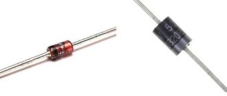
Low-power zener diode device
with flexible leads in plastic (top) and glass (bottom) cases
Fig. Device of a low-power zener diode with flexible leads in a plastic case.
Rice. The device of a low-power zener diode with flexible leads in a glass case
Low-voltage zener diodes (with low base resistance) are more likely to have a tunnel breakdown. For zener diodes with a high-resistance base, the breakdown is of an avalanche nature. To ensure electrical breakdown at relatively low reverse voltages, the electric field strength in the pn junction must be significantly higher than that of conventional diodes, therefore, in the manufacture of zener diodes, materials with a high concentration of impurities are used.
Marking of zener diodes
Domestic and imported zener diodes in a metal case are marked simply and clearly. They are marked with the name of the device and the location of the anode and cathode in the form of a schematic designation.
Devices in a plastic case are marked with rings and dots of various colors on the cathode and anode sides. You can determine the type of device by the color and combination of symbols, but to do this you will have to look in reference books or use calculator programs. Both can be found on the Internet.
Sometimes stabilization voltage is applied to low-power zener diodes.
Basic parameters of zener diodes
1. Ust 2. Differential resistance Rdif = 0.5 – 200 Ohm 3. Ist min stabilization current minimum 4. Ist max stabilization current maximum Imax≈ Pmax/Ust Silicon diodes are used as zener diodes, which are highly resistant to thermal breakdown. Silicon zener diodes are used to stabilize voltages of power supplies, as well as to fix U levels in various circuits. Groups of low-power diodes in the form of diode matrices and diode assemblies are used in logic devices, decoders and other VT elements. A zener diode is usually included in the stabilization circuit so that the pn junction is reverse biased. To stabilize low voltages U = 1 - 1.5V, stabistors are used
Main characteristics of a zener diode
To select a Zener diode for existing purposes, you need to know several important parameters. These characteristics will determine the suitability of the selected device for solving the assigned tasks.
Rated stabilization voltage
The first zener parameter that you need to pay attention to when choosing is the stabilization voltage, determined by the point at which the avalanche breakdown begins. This is where the choice of device to use in the circuit begins. For different instances of ordinary zener diodes, even of the same type, the voltage has a spread of around several percent; for precision ones, the difference is lower. If the nominal voltage is unknown, it can be determined by constructing a simple circuit. You should prepare:
- ballast resistor 1…3 kOhm;
- adjustable voltage source;
- voltmeter (you can use a tester).
It is necessary to increase the voltage of the power source from zero, monitoring the increase in voltage on the zener diode using a voltmeter. At some point it will stop, despite further increasing the input voltage. This is the actual stabilization voltage. If there is no regulated source, you can use a power supply with a constant output voltage obviously higher than Ustabilization. The measurement scheme and principle remain the same. But there is a risk of the semiconductor device failing due to exceeding the operating current.
Zener diodes are used to work with voltages from 2...3 V to 200 V. To generate a stable voltage below this range, other devices are used - stabistors, operating in the direct section of the current-voltage characteristic.
Precision and bidirectional zener diodes
Precision zener diodes use three series-connected pn junctions, one of which is stabilizing, the other two are temperature-compensating. If the stabilizing junction operates in the avalanche breakdown mode, then the voltage across it increases with increasing temperature. At the same time, the forward voltage at two temperature-compensating junctions decreases, so the total voltage at the zener diode changes slightly.
To ensure stabilization of bipolar voltages, general-purpose zener diodes are connected in series, and precision ones are connected in parallel.
Double-anode zener diodes have a structure formed by the diffusion of impurities into the n-silicon wafer from both sides simultaneously. The resulting two pn junctions are connected back to back. Only the anode p-regions of the structure have external leads. When a voltage of any polarity is applied to the zener diode, one junction operates in the electrical breakdown mode, and the other is thermally compensating
Application areas of zener diodes and stabilizers
The good stabilizing properties of zener diodes and stabilizers determine the main area of application of these radio components - the creation of a fixed supply and reference voltage in various radio-electronic devices. In first place in terms of prevalence are zener diodes used in power supplies. The use of these specialized diodes ensures stable output voltage parameters and at the same time simplifies the circuit. In power supplies with increased requirements for the accuracy of output characteristics, precision zener diodes are used. These elements are installed in high-precision measuring equipment and analog-to-digital converters. Double-node zener diodes are used in impulse noise suppressors. These radio components in real circuits are often combined with pulsed diodes. High-speed zener diodes in combination with microwave diodes are used in equipment operating at ultra-high frequencies - transmitters, radars, and so on.
Protective zener diodes in a “smart” MOS transistor of the Intelligent Power Switch family from International Rectifier
The main area of application of a zener diode is stabilizing the DC voltage of power supplies. In the simplest circuit of a linear parametric stabilizer, the zener diode acts as both a source of reference voltage and a power control element. In more complex circuits, the zener diode is assigned only the function of a reference voltage source, and the regulating element is an external power transistor.
Precision temperature-compensated zener diodes and zener diodes with a hidden structure are widely used as discrete and integrated reference voltage sources, including in the most demanding voltage stability circuits of measuring analog-to-digital converters. From the mid-1970s to the present day (2012), zener diodes with a hidden structure have been the most accurate and stable solid-state ionizers. The accuracy of laboratory voltage standards using specially selected integrated zener diodes approaches those of a normal Weston element[38].
Special pulse avalanche zener diodes (“transient impulse suppressors”, “suppressors”, “TVS diodes”) are used to protect electrical equipment from overvoltages caused by lightning discharges and static electricity, as well as from voltage surges on inductive loads. Such devices with a nominal power of 1 W can withstand current pulses of tens and hundreds of amperes much better than “ordinary” fifty-watt power zener diodes. To protect the inputs of electrical measuring instruments and the gates of field-effect transistors, conventional low-power zener diodes are used. In modern “smart” MOS transistors, protective zener diodes are made on the same chip with the power transistor.
In the past, zener diodes also performed other tasks, which subsequently lost their former significance:
- Limitation, shaping, amplitude selection and detection of pulses. Even in the era of vacuum tubes, silicon zener diodes were widely used to limit the amplitude of pulses and convert signals of arbitrary shape into pulses of a given polarity. With the development of integrated technologies, this function was taken over by devices based on high-speed comparators, and then by digital signal processors.
- Stabilizing the AC voltage also came down to limiting the swing of the sinusoidal voltage with a double-sided zener diode. When the input voltage changed, the amplitude of the output voltage was maintained constant, and its effective value only slightly lagged behind the effective value of the input voltage.
- Setting the relay actuation voltages. If it was necessary to set a non-standard response threshold of the relay, a zener diode was connected in series with its winding, which brought the response threshold to the required value. With the development of semiconductor switching circuits, the scope of application of relays has narrowed, and the function of relay control has been taken over by transistor and integrated threshold circuits.
- Setting the operating points of the amplifier stages. Tube amplifiers of the 1960s used zener diodes as a replacement for RC auto-bias networks. At lower frequencies of the audio range and at infrasonic frequencies, the design capacitances of the capacitors of such circuits became unacceptably large, so the zener diode became an economical alternative to an expensive capacitor.
- Interstage level shift. Level shifting in DC tube amplifiers was usually accomplished using gas-filled zener diodes or conventional neon lamps. With the invention of semiconductor zener diodes, they began to be used instead of gas-filled ones. Similar solutions were used in transistor equipment, but were quickly replaced by more advanced level shift circuits on transistors.
- Zener diodes with high TKN have been used as temperature sensors in bridge measuring circuits. As supply voltages and power consumption decreased, forward biased diodes, transistor PTAT circuits, and integrated circuits based on them took over this function.
In the SPICE modeling environment, the model of an elementary zener diode is used not only for its intended purpose, but also to describe the breakdown mode in models of “real” bipolar transistors. The standard SPICE model of the Ebers-Moll transistor does not consider the breakdown mode