A field-effect (unipolar) transistor is a device that has three terminals and is controlled by a voltage applied to the control electrode (gate). The regulated current flows through the source-drain circuit.
The idea of such a triode arose about 100 years ago, but it became possible to approach practical implementation only in the middle of the last century. In the 50s of the last century, the concept of a field-effect transistor was developed, and in 1960 the first working sample was manufactured. To understand the advantages and disadvantages of triodes of this type, you need to understand their structure.
Classification of field effect transistors
Let's start with the classification. There are numerous types of field-effect transistors, each working according to an algorithm:
- Channel conductivity type: n or p. The factor determines the polarity of the control voltage.
- By structure. With p-n junction alloy, diffusion, MIS (MOS), with Schottky barrier, thin film.
- The number of electrodes is 3 or 4. In the latter case, the substrate is considered a separate entity, allowing you to control the flow of current through the channel (in addition to the gate).
- Conductor material. Today, silicon, germanium, and gallium arsenide are common. The semiconductor material is marked with a symbol such as letters (K, G, A) or (in military industry products) numbers (1, 2, 3).
- The application class is not included in the marking; it is indicated by reference books that provide information that the field-effect transistor is often included in amplifiers and radio receivers.
In world practice, there is a division according to applicability into the following 5 groups: high-frequency, low-frequency, direct current amplifiers, modulators, key ones. Semiconductor transistor - The range of electrical parameters determines the set of values in which the field-effect transistor remains operational. Voltage, current, frequency.
- Based on their design features, they are divided into unitrons, alkatrons, teknetrons, and gridistors. Each device is equipped with key features. Alkatron electrodes are made of concentric rings, increasing the volume of current passed.
- Based on the number of structural elements contained in one substrate, they are classified as double, complementary.
In addition to the general classification, a specialized one has been invented that defines the principles of operation. There are:
- Field-effect transistors with control pn junction.
- Field effect transistors with a Schottky barrier.
- Insulated gate field effect transistors:
- With built-in channel.
- With induced channel.
In the literature, structures are further ordered as follows: it is not practical to use the MOS designation; oxide structures are considered a special case of MOS (metal, dielectric, semiconductor). The Schottky barrier (MeP) should be highlighted separately, since it is a different structure. Reminds the properties of a pn junction. Let us add that, structurally, the transistor can simultaneously contain a dielectric (silicon nitride) and an oxide (tetravalent silicon), as happened with KP305. Such technical solutions are used by people looking for methods to obtain unique properties of a product and reduce the cost.
FET devices
Among foreign abbreviations for field-effect transistors, the combination FET is reserved, sometimes denoting the type of control - with a pn junction. In the latter case, we will also encounter JFET. Synonymous words. Abroad, it is customary to separate oxide (MOSFET, MOS, MOST - synonyms), nitride (MNS, MNSFET) field-effect transistors. The presence of a Schottky barrier is marked by SBGT. Apparently, the material is significant, domestic literature is silent about the significance of the fact.
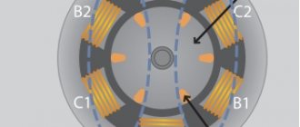
The electrodes of field-effect transistors in the diagrams are designated: D (drain) - drain, S (source) - source, G (gate) - gate. The substrate is usually called substrate.
Output characteristics
The family of output characteristics of a transistor with a control pn junction in a common-source circuit is shown in Fig. 26.4. They are similar to the output characteristics of a bipolar transistor. These characteristics show the dependence of the output current ID on the output voltage VDS (voltage between drain and source) for a given value of gate voltage VGS (voltage between gate and source).
The range of variation of the gate-source bias voltage is quite large (several volts), in contrast to a bipolar transistor, where the base-emitter voltage is almost constant. It can be seen that as the gate voltage increases (in absolute value), the drain current decreases. This reduction occurs until the expanding depletion layer of the gate-channel junction closes the entire channel, stopping current flow. In this case, the field effect transistor is said to be in the cutoff state.
Field effect transistor circuit.
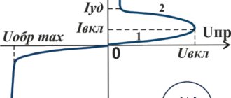
Cut-off voltage
Let's consider the output characteristic for VGS = 0. As the voltage VDS increases (from zero value), the drain current gradually increases until it reaches point P, after which the current value practically does not change. The voltage at point P is called the cut-off voltage. At this voltage, the depletion layer associated with the reverse-biased gate-channel junction almost completely blocks the channel. However, the flow of current ID at this point does not stop, since it is thanks to this current that the depletion layer is created. All curves of the family of output characteristics have their own cut-off points: P1, P2, etc. If you connect these points to each other with a line, then to the right of it lies the cut-off region, which is the working region of the field-effect transistor.
Field-effect transistor.
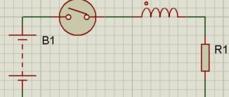
Common-source field-effect transistor amplifier
The circuit of a typical AF amplifier using a field-effect transistor is shown in Fig. 26.5. In this circuit, very little gate leakage current is diverted to the chassis through leakage resistor R1. Resistor R3 provides the necessary reverse bias, raising the source potential above the gate potential. In addition, this resistor also ensures the stability of the amplifier's DC mode. R2 is a load resistor that can have a very high resistance (up to 1.5 MOhm). Decoupling capacitor C2 in the source circuit eliminates negative AC feedback through resistor R3. It should be noted that the decoupling capacitor C1 may have a small capacitance (0.1 μF) due to the high input resistance of the field-effect transistor.
It will be interesting➡ What is a bipolar transistor
When a signal is applied to the input of the amplifier, the drain current changes, causing, in turn, a change in the output voltage at the drain of the transistor. During the positive half-cycle of the input signal, the gate voltage increases in the positive direction, the reverse bias voltage of the gate-source junction decreases and hence the current ID of the FET increases. An increase in ID leads to a decrease in the output (drain) voltage, and the negative half-cycle of the amplified signal is reproduced at the output. Conversely, a negative half-cycle of the input signal corresponds to a positive half-cycle of the output signal. Thus, the input and output signals of a common-source amplifier are out of phase.
Field effect transistor device
The control electrode of the field effect transistor is called the gate. The channel is formed by a semiconductor of arbitrary conductivity type. Depending on the polarity of the control voltage, it is positive or negative. The field of the corresponding sign displaces free carriers until the isthmus under the gate electrode is completely empty. Achieved by applying a field to either a pn junction or a homogeneous semiconductor. The current becomes zero. This is how a field effect transistor works.
The current flows from source to drain; beginners are traditionally tormented by the question of distinguishing between the two indicated electrodes. There is no difference in which direction the charges move. The field effect transistor is reversible. The unipolarity of charge carriers explains the low noise level. Therefore, field-effect transistors occupy a dominant position in technology.
Transistor design
The key feature of the devices is the large input resistance, especially for alternating current. An obvious fact arising from the control of a reverse-biased pn junction (Schottky junction), or the capacitance of a process capacitor in the area of an insulated gate.
The substrate is often an undoped semiconductor. For field effect transistors with a Schottky gate - gallium arsenide. In its pure form, it is a good insulator, to which the following requirements are imposed as part of the product:
- Absence of negative phenomena at the interface with the channel, source, drain: photosensitivity, parasitic control on the substrate, hysteresis of parameters.
- Thermal stability during technological cycles of product manufacturing: resistance to annealing, epitaxy. No diffusion of impurities into the active layers, resulting in degradation.
- Minimum impurities. The requirement is closely related to the previous one.
- High-quality crystal lattice, minimum defects.
It is difficult to create a layer of significant thickness that meets the list of conditions. Therefore, a fifth requirement is added, which consists in the possibility of gradually growing the substrate to the desired size.
Comparison of IGBT with MOSFET
The structures of both transistors are very similar to each other. Regarding current flow, an important difference is the addition of a P-type substrate layer under the N-type substrate layer in the IGBT module structure. In this additional layer, holes are introduced into the high-resistance N-type layer, creating an excess of carriers. This increase in conductivity in the N-layer helps reduce the overall on-state voltage in the IGBT module. Unfortunately, this also blocks the flow of electricity in the opposite direction. Therefore, a special diode is added to the circuit, which is located in parallel with the IGBT to conduct current in the opposite direction.
The MOSFET can switch at higher frequencies, however there are two limitations: the time it takes for the electrons to be transported in the drift region and the time it takes to charge/discharge the input gate and its capacitance. However, these transistors typically achieve higher switching frequencies than IGBT modules.
Field effect transistors with control pn junction and MeP
In this case, the conductivity type of the gate material is different from that used by the channel. In practice you will see various improvements. The shutter is composed of five areas recessed into the channel. A lower voltage can control the flow of current. Meaning an increase in gain.
Bipolar transistor
The circuits use reverse bias of the pn junction; the stronger, the narrower the channel for current flow. At a certain voltage value the transistor turns off. Forward bias is dangerous to use because the powerful drive circuit can affect the gate contour. If the junction is open, a large current will flow or a high voltage will be applied. Normal mode is ensured by the correct selection of polarity and other characteristics of the power source, and the choice of the operating point of the transistor.
However, in some cases forward gate currents are intentionally used. It is noteworthy that this mode can be used by those MOS transistors where the substrate forms a pn junction with the channel. The moving source charge is divided between the gate and drain. You can find a region where a significant current gain is obtained. The mode is controlled by the shutter. As the current iz increases (up to 100 μA), the circuit parameters deteriorate sharply.
A similar connection is used by the so-called gate frequency detector circuit. The design exploits the rectifying properties of the pn junction between the gate and channel. There is little or no forward bias. The device is still driven by gate current. In the drain circuit, a significant signal amplification is obtained. The rectified voltage for the gate is a blocking voltage and varies according to the input law. Simultaneously with detection, signal amplification is achieved. The drain circuit voltage contains the components:
- Constant component. Not used at all.
- Signal with carrier frequency. It is planted on the ground using filter containers.
- Signal with the frequency of the modulating signal. Processed to extract embedded information.
The disadvantage of a gate frequency detector is considered to be a large coefficient of nonlinear distortion. Moreover, the results are equally bad for weak (quadratic dependence of the operating characteristic) and strong (entering the cutoff mode) signals. Somewhat better are demonstrated by a phase detector based on a two-gate transistor. A reference signal is supplied to one control electrode, and an information component is formed at the drain, amplified by a field-effect transistor.
Despite the large linear distortions, the effect is used. For example, in selective power amplifiers that transmit a narrow spectrum of frequencies in doses. Harmonics are filtered and do not have a big impact on the final quality of the circuit.
Metal-semiconductor (MeS) transistors with a Schottky barrier are almost no different from those with a pn junction. At least when it comes to operating principles. But thanks to the special qualities of the metal-semiconductor transition, products are capable of operating at higher frequencies (tens of GHz, cutoff frequencies in the region of 100 GHz). At the same time, the MeP structure is easier to implement when it comes to production and technological processes. Frequency characteristics are determined by the gate charging time and carrier mobility (for GaAs over 10,000 sq. cm/V s).
Briefly about IGBT
The IGBT module is also a fully controlled switch with three pins (gate, collector and emitter). Its control signal is supplied between the gate and emitter and the load between the collector and emitter.
An IGBT combines the simple gate driving characteristics of a MOSFET with the high current, low saturation voltage nature of a bipolar transistor. This is achieved by using an isolated field-effect transistor for the control input and a bipolar power transistor as a high-current switch.
The IGBT module is specially designed for fast switching on and off. In fact, the pulse repetition rate reaches the ultrasonic range. This unique ability makes IGBTs often used in Class D amplifiers to synthesize complex signals with pulse width modulation and low-pass filters. They are also used to generate high-power pulses in fields such as particle physics and plasma, and play an important role in modern devices such as electric cars, electric bicycles, trains, variable-speed refrigerators, air conditioners and much more.
MOS transistors
In MIS structures, the gate is reliably isolated from the channel, and control occurs entirely due to the influence of the field. Insulation is carried out using silicon oxide or nitride. It is these coatings that are easier to apply on the surface of the crystal. It is noteworthy that in this case there are also metal-semiconductor junctions in the source and drain regions, as in any polar transistor. Many authors forget about this fact, or mention it in passing by using the mysterious phrase ohmic contacts.
This question was raised in the topic about the Schottky diode. A barrier does not always appear at the junction of metal and semiconductor. In some cases the contact is ohmic. This depends largely on the characteristics of technological processing and geometric dimensions. The technical characteristics of real devices strongly depend on various defects of the oxide (nitride) layer. Here are some:
- The imperfection of the crystal lattice in the surface region is due to broken bonds at the boundary of the change of materials. The influence is exerted both by free atoms of the semiconductor and by impurities like oxygen, which is present in any case. For example, when using epitaxy methods. As a result, energy levels appear that lie deep in the band gap.
- At the interface between the oxide and the semiconductor (3 nm thick), an excess charge is formed, the nature of which has not yet been explained. Presumably, the role is played by positive free spaces (holes) of defect atoms of the semiconductor itself and oxygen.
- The drift of ionized atoms of sodium, potassium and other alkali metals occurs at low voltages at the electrode. This increases the charge accumulated at the layer boundaries. To block this effect, phosphorus oxide (anhydride) is used in silicon oxide.
The positive volume charge in the oxide affects the threshold voltage at which the channel is unlocked. The parameter determines the switching speed and determines the leakage current (below the threshold). In addition, the gate material, the thickness of the oxide layer, and the concentration of impurities affect the operation. So the result again comes down to technology. To obtain a given mode, materials, geometric dimensions, and a manufacturing process with low temperatures are selected. Certain techniques will also reduce the number of defects, which has a beneficial effect on reducing parasitic charge.