ATX power supply, device and principle of operation. Part 1.
Since the power supply is an integral part of the PC, it will be interesting for every person involved in electronics and not only to know more about it.
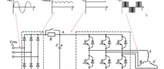
The performance of the PC as a whole directly depends on the quality of the power supply. And so, I believe that we need to start with the simplest, for what purpose the power supply is intended: - generating the supply voltage for PC components: +3.3 +5 +12 Volts (additionally -12V and -5V); - galvanic isolation between 220 and the PC (so that there is no electric shock, and there are no current leaks when pairing components). A simple example of galvanic isolation is a transformer. But to power a PC, you need a lot of power, and therefore a large transformer (the computer would be very large :), and two people would have to carry it due to its considerable weight, but we avoided this :)). To build compact blocks, an increased frequency of the transformer supply current is used; as the frequency increases, the same magnetic flux in the transformer requires a smaller cross-section of the magnetic circuit and fewer turns. The creation of light and compact power supplies allows the frequency of the transformer supply voltage to be increased by 1000 times or more. The basic principle of operation of the power supply is as follows: the conversion of alternating mains voltage (50 Hz) into AC. a high-frequency voltage of a rectangular shape (if an oscilloscope could show an example), which is lowered using a transformer, then rectified and filtered. Block diagram of a pulse power supply.
1. Block Converts 220V variable to constant. The composition of such a block is: a diode bridge for rectifying alternating voltage + a filter for smoothing ripples of the rectified voltage. There should also be (in cheap power supplies they save money by not soldering them, but I immediately recommend installing them when remodeling or repairing) a network voltage filter from the ripples of the pulse generator, as well as thermistors to smooth out the current surge when turned on. In the picture, the filter is indicated by a dotted line in the diagram; we will see it in almost any power supply circuit (but not always on the board :)). 2. Block This block generates pulses of a certain frequency that feed the primary winding of the transformer. The frequency of generating pulses from various power supply manufacturers is somewhere in the range of 30-200 kHz. 3. Block The transformer has the following functions: - galvanic isolation; — reducing the voltage on the secondary windings to the required level. 4. Block This block converts the voltage received from block 3 into DC. It consists of voltage-rectifying diodes and a ripple filter. The filter consists of a choke and a group of capacitors. Often, to save money, capacitors are installed with low capacitance and chokes with low inductance.
Pulse generator in more detail.
The RF converter circuit consists of powerful transistors that operate in switch and pulse transformer mode. The power supply can be a single-cycle or push-pull converter: - single-cycle: one transistor opens and closes; - push-pull: two transistors alternately open and close. Let's look at the drawing.
Circuit elements: R1 - resistance that sets the bias on the keys. Necessary for a more stable start of the oscillation process in the converter. R2 is a resistance that limits the base current on the transistors and is necessary to protect the transistors from failure. TP1 - Transformer with three groups of windings. The first generates the output voltage. The second serves as a load for transistors. The third generates the control voltage for the transistors. When the first circuit is turned on, the transistor is slightly open, because a positive voltage is applied to the base through resistor R1. A current flows through the slightly open transistor, which flows through winding II. The current creates a magnetic field. The magnetic field creates voltage in the remaining windings. A positive voltage is created on winding III, which opens the transistor even more. The process continues until the transistor enters saturation mode. The saturation mode is characterized by the fact that when the applied control current to the transistor increases, the output current remains unchanged. Only when the magnetic field changes is voltage generated on the windings; if there are no changes on the transistor, the EMF in windings II and III will also disappear. When the voltage on winding III disappears, then the opening of the transistor will decrease, and therefore the output current of the transistor and the magnetic field will decrease, which will lead to the appearance of a voltage of the opposite polarity. Negative voltage on winding III will close the transistor even more. The process continues until the magnetic field disappears completely. When the field disappears, the negative voltage will disappear and the process will begin in a circle again. A push-pull converter works the same way, but since it has two transistors operating alternately, this application increases the efficiency of the converter and improves its performance. Mostly they use two-stroke ones, but if you need low power and dimensions, as well as simplicity, then single-stroke ones. The converters discussed above are complete devices, but their use is complicated by the variation of various parameters such as: output load, supply voltage, and temperature of the converter.
Control of keys by PWM controller (494).
The converter consists of transformer T1 and transistor VT1. The mains voltage is supplied through a mains filter (SF) to a mains rectifier (RM) diode bridge, filtered by a capacitor SF and supplied through winding W1 to the collector of transistor VT1. When a rectangular pulse is applied to the base of the transistor, it opens and current Ik flows through it, which increases. The same current flowing through the primary winding of transformer T1 leads to an increase in the magnetic flux in the transformer core and induced self-inductive emf in the secondary winding W2. As a result, a positive voltage will appear on the VD diode. By increasing the duration of the pulse based on transistor VT1, the voltage in the secondary circuit will increase, and if you decrease the duration, the voltage will decrease. By changing the pulse duration on the base of the transistor, we change the output voltage on the W1 winding of T1, and stabilize the output voltages of the power supply. We need a circuit for generating trigger pulses and controlling their duration (latitude). This circuit uses a PWM (pulse width modulation) controller. The PWM controller consists of: - a master pulse generator (which determines the operating frequency of the converter); — control circuits; — a logical circuit that controls the pulse duration; — protection schemes. This is the topic of another article. In order to stabilize the output voltages of the power supply unit, the PWM controller circuit “must know” the magnitude of the output voltages. For this, a feedback circuit (or tracking circuit) is used, made on optocoupler U1 and resistor R2. An increase in voltage in the secondary circuit of transformer T1 will lead to an increase in the intensity of the LED radiation, and therefore a decrease in the junction resistance of the phototransistor (part of the optocoupler U1). This leads to resistor R2 connected in series with the phototransistor to an increase in the voltage drop and a decrease in the voltage at pin 1 of the PWM switch. A decrease in voltage causes the logic circuit that makes up the PWM to increase the pulse duration until the voltage at pin 1 matches the specified parameters. The process is reversed when the voltage decreases. There are two implementations of feedback circuits: - “direct” in the diagram above, feedback is removed directly from the secondary rectifier; - “indirect” is removed directly from the additional winding W3 (see figure below); A change in voltage on the secondary winding will lead to a change in it on winding W3, which is transmitted through R2 to 1 pin of the PWM switch.
Below is a real power supply diagram.
1. The block rectifies and filters alternating voltage, and there is also a filter against interference created by the power supply itself. 2. Block This block generates +5VSB (standby voltage) and also powers the PWM controller. 3. Block The third block (PWM - controller 494) contains the following functions: - control of transistor switches; — stabilization of output voltages; — short circuit protection. 4. Block This block includes two transformers and two groups of transistor switches. The first transformer generates the control voltage for the output transistors. 1 group of transistors amplifies the generated signal TL494 and transmits it to the first transformer. Group 2 of transistors is loaded onto the main transformer, on which the main supply voltages are formed. 5. Block This block includes Schottky diodes to rectify the output voltage of the transformer, as well as a low-pass filter. The low-pass filter includes electrolytic capacitors of large capacities (depending on the power supply manufacturer) and chokes, as well as resistors for discharging these capacitors when the power supply is turned off.
A little about the duty room.
The differences between ATX standard units and AT standard power supplies are that ATX standard power supplies have a standby supply voltage source. At pin 9 (20 pin, purple wire) of the connector, a voltage of +5VSB is generated which goes to the motherboard to power the power supply control circuit. This circuit generates the “PS-ON” signal (pin 14 of the connector, green wire).
In this circuit, the converter operates at a frequency determined mainly by the parameters of transformer T3 and the values of the elements in the base circuit of the key transistor Q5 - the capacitance of capacitor C28 and the resistance of the initial bias resistor R48 [1]. Positive feedback to the base of transistor Q5 comes from the auxiliary winding of transformer T2 through elements C28 and R51. The negative voltage from the same winding after the rectifier on elements D29 and C27, if it exceeds the stabilization voltage of the zener diode ZD1 (in this case 16 V), is also supplied to the base Q5, prohibiting the operation of the converter. In this way, the output voltage level is monitored. The supply voltage from the mains rectifier is supplied to the converter through the current-limiting resistor R45, which, if it fails, can be replaced with a 500 mA fuse or eliminated altogether. In the circuit in Fig. 1, resistor R56 with a nominal value of 0.5 Ohm, connected to the emitter of transistor Q5, is a current sensor; when the current of transistor Q5 exceeds the permissible value, the voltage from it through resistor R54 goes to the base of transistor Q9 of type 2SC945, opening it, and thereby prohibiting the operation of Q5 . In a similar way, additional protection is provided for Q5 and the primary winding T3. Chain R47C29 serves to protect transistor Q5 from voltage surges. KSC5027 transistors are used as the key transistor Q5 in the specified power supply model. In my previous article, the power supply was based on similar elements (duty room).
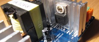
Now let’s look at the power supply unit live.
1. Elements of a network filter against interference generated by power supply units. 2. Diode bridge rectifying 220V variables. 3. Mains voltage filter capacitances. 4. Radiator for the output transistors of the converter, as well as the transistor of the duty converter. 5. Main transformer: isolation from the network and generation of all voltages. 6. Transformer for generating the control voltage of the output transistors. 7. Converter transformer that generates standby voltage. 8. Radiator for Schottky diodes. 9. PWM controller chip. 10. Output voltage filters (electrolytic capacitors). 11. Output voltage filter chokes.
I'll stop there for now. Thank you all for your attention for so long. I hope it was useful to at least someone. I look forward to comments and suggestions for additions. To be continued…
We give a definition
A power supply is a device whose task is to convert AC mains voltage into DC and supply it to computer components (system card, processor, video card, hard drive, RAM and other peripheral devices).
Also, the power supply unit (PSU) has the ability to protect the computer from voltage surges.
Essentially, this is an inverter system (pulse-type devices) that inverts and changes the mains voltage for different tasks.
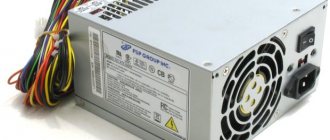
The PSU looks like a small box with a fan inserted into the system unit.
In different countries, the voltage and frequency of the current in the network are different. For example, if in Russia, as well as in most European countries, these indicators are 220V and 50 Hz, respectively, then in the USA the voltage in the network is 120V and the frequency is 60Hz.
For example, in Australia these figures are 240V/50Hz.
Accordingly, the production of power supplies, in technical terms, is adjusted based on which country in the world they will be supplied to.
There are universal devices that can be used in some countries.
Without a power supply, the computer will not work. Very often, if the system unit does not turn on, you should first look for the reason in this device, and, if necessary, replace it with a new one.
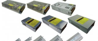
Today there are devices with different capacities.
The power supply of modern laptops, for example, is 25-100 watts. In ordinary personal computers, the parameter sometimes reaches 2000 Watts.
They say that the more powerful the device, the better. However, not everyone needs such a powerful and expensive device.
Many experts regard the purchase of a high-power power supply as a waste of money (including on electricity).
Some companies today refuse to produce such high-power devices due to environmental problems in the world.
Although the presence of devices on store shelves with a power of 500 watts is commonplace in our time.
Accessories
These are perhaps the most modern control devices in DC circuits. It can be compared to a transformer, since the behavior of a pulse converter is similar to a transformer with a smoothly varying number of turns:
The big advantage of such devices is that they can recuperate energy into the network, smoothly regulate the rate of current rise, and have high efficiency and speed.
Useful tips Connection diagrams Principles of operation of devices Main concepts Meters from Energomer Precautions Incandescent lamps Video instructions for the master Testing with a multimeter
A simple two-polar voltage regulator on LM317.
The device is based on the circuit described above, and a negative voltage stabilization arm is added.
Characteristics and advantages of a two-polar stabilizer
- stabilization voltage from 1.2 to 30 V;
- maximum current up to 5 A;
- a small number of elements are used;
- simplicity in choosing a transformer, since you can use the secondary winding without a central tap;
The parts are installed on one-sided fiberglass. Transistor VT1, VT2 and microcircuits LM317 and LM337 should be installed on radiators. When installing on a common radiator, insulating gaskets and bushings should be used.
Switching power supply
The UPS itself was structurally assembled in the case of the same disassembled ATX power supply. Transistors VT3,VT4 are installed on radiators with an area of 50 cm 2.
Expert opinion
It-Technology, Electrical power and electronics specialist
Ask questions to the “Specialist for modernization of energy generation systems”
Do-it-yourself power supply: 100 photos, drawings and the best projects with adjustment Transformers are small in size and weight when using a pulse unit due to the fact that increasing the frequency makes it possible to increase their operating efficiency and also reduce the thickness of the core. Ask, I'm in touch!
Current and voltage regulator
The DC controller can function normally at a maximum temperature of 40C. This factor must be taken into account during operation. Field-effect transistors are located next to thyristors, since they only pass current in one direction. Due to this, the negative resistance will be maintained at a level not exceeding 8 ohms.
During adjustments in the network, smooth current stabilization must be ensured. At high loads, the circuit is supplemented with reverse direction zener diodes. To connect them together, transistors and an inductor are used. Thus, the current regulator on the transistor performs current conversion quickly and losslessly.
Expert opinion
It-Technology, Electrical power and electronics specialist
Ask questions to the “Specialist for modernization of energy generation systems”
Installation step by step Namely, this is the TL494 microcircuit, capacitors C9, C10, diode bridge VDS1, capacitors C1, C2, C5, C6, C7, diode VD2, Schottky diodes VD3, VD4, and ferrite cores with frames TR1, TR2. Ask, I'm in touch!
Network switching power supply
Network switching power supply (Fig. 3) is designed for telephone sets with automatic caller identification or for other devices with a power consumption of 3...5W, powered by a voltage of 5...24V.
The power supply is protected against output short circuit. The instability of the output voltage does not exceed 5% when the supply voltage changes from 150 to 240 V and the load current is within 20... 100% of the nominal value. A controlled pulse generator provides a signal with a frequency of 25...30 kHz based on the VT3 transistor. Chokes L1, L2 and L3 are wound on magnetic cores of type K10x6x3 from pressed permalloy MP140. The inductor windings L1, L2 contain 20 turns of 0.35 mm PETV wire and are each located on its own half of the ring with a gap between the windings of at least 1 mm.
Choke L3 is wound with 0.63 mm PETV wire turn to turn in one layer along the inner perimeter of the ring. Transformer T1 is made on a magnetic core B22 made of M2000NM1 ferrite.
Rice. 3. Diagram of a network switching power supply.
Its windings are wound on a collapsible frame turn to turn with PETV wire and impregnated with glue. The first winding I is wound in several layers, containing 260 turns of 0.12 mm wire. A shielding winding with one terminal is wound with the same wire (shown with a dotted line in Fig. 3), then BF-2 glue is applied and wrapped with one layer of Lakot-kani.
Winding III is wound with 0.56 mm wire. For an output voltage of 5V, it contains 13 turns. Winding II is wound last. It contains 22 turns of wire 0.15...0.18 mm. A non-magnetic gap is provided between the cups.
Switching power supply with microcircuit
The diagram of a power supply with a microcircuit from the same company Power Integration is shown in Fig. 6. The device uses a semiconductor voltage limiter - 1.5KE250A.
The converter provides galvanic isolation of the output voltage from the mains voltage. With the ratings and elements indicated in the diagram, the device allows you to connect a load that consumes 20 W at a voltage of 24 V. The efficiency of the converter approaches 90%. Conversion frequency - 100 Hz. The device is protected from short circuits in the load.
Rice. 6. Circuit diagram of a 24V switching power supply on a microcircuit from Power Integration.
The output power of the converter is determined by the type of microcircuit used, the main characteristics of which are given in Table 1.
Table 1. Characteristics of TOP221Y - TOP227Y series microcircuits.
| Chip type | Рmax, W | Protection current, A | Open transistor resistance, Ohm |
| TOP221Y | 7 | 0,25 | 31,2 |
| T0P222Y | 15 | 0,5 | 15,6 |
| T0P223Y | 30 | 1 | 7,8 |
| T0P224Y | 45 | 1,5 | 5,2 |
| T0P225Y | 60 | 2 | 3,9 |
| T0P226Y | 75 | 2,5 | 3,1 |
| T0P227Y | 90 | 3 | 2,6 |