Zener diode refers to one of the used radio-electronic elements. Each more or less high-quality power supply contains a voltage stabilization unit, which can change when the load resistance changes or when the input voltage deviates from the nominal value.
Voltage stabilization is performed mainly to ensure normal operation of the remaining radio elements of the device, for example microcircuits, transistors, microcontrollers, etc.
Zener diodes are widely used in low-power power supplies or in individual units, the power of which rarely exceeds tens of watts.
The main advantage of zener diodes is their low cost and size, so they still cannot be replaced by integrated voltage stabilizers such as LM7805 or 78L05, etc.
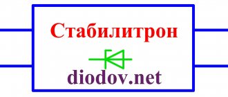
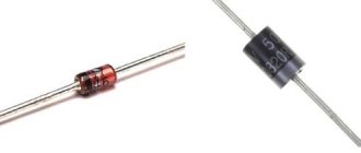
A zener diode is very similar to a diode because its semiconductor crystal is housed in a similar package.
The conventional graphic designation of a zener diode on electrical circuit drawings is also similar to the designation of a diode, only on the cathode side a short horizontal line is added, directed towards the anode.
The principle of operation of a zener diode
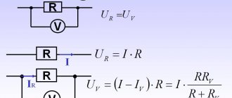
Let's consider the principle of operation of a zener diode using the example of its connection circuit and current-voltage characteristic. To perform its main function, the zener diode VD is connected in series with a resistor Rb and together they are connected to a source of unstabilized input voltage Uin. The already stabilized output voltage Uout is removed only from pins 2, 3 VD. Therefore, the load Rн is connected to the corresponding points 2 and 3. As can be seen from the diagram, VD and Rb form a voltage divider. Only the resistance of the zener diode does not have a constant value and is called dynamic, since it depends on the amount of electric current flowing through the semiconductor device.
The voltage Uin supplied to the zener diode from the resistors must be at least a couple of volts higher than the output voltage Uout, otherwise the semiconductor device VD will not open and will not be able to perform its main function.
Let's say that at some arbitrary point in time at outputs 1 and 3 the value of Uin began to increase. The following processes will begin to occur in the circuit. As the voltage increases, according to Ohm's law, the current will begin to increase, let's call it the input current Iin. As the current increases, the voltage drop across the resistor Rb will increase, and at VD it will remain unchanged (this will be explained further in the characteristic), therefore Uout will remain at the same level. Consequently, the increase in input voltage will drop or be extinguished by resistor Rb. Therefore, Rb is called damping or ballast.
Now, let’s say the load has changed, for example, the resistance Rн has decreased, and the current In will increase accordingly. In this case, the current flowing through the zener diode Ist will decrease, and Iin will remain virtually unchanged.
Level fixation circuit
Diode clipping
The limiter cuts off the top of the signal and makes it flat. The restriction can be unilateral or bilateral. So, the diagram in Fig. 28.10 limits only the negative half-wave voltage. The voltage drop across the diode when connected directly will create a negative voltage level of –0.6 V, shown in the dotted line. Typically, diodes are considered ideal and this voltage is neglected.
To obtain voltage limitation at other levels, a battery is connected in series with the diode. In this case, the diode can be biased in the forward (Fig. 28.11(a)) or reverse (Fig. 28.11(b)) direction. In the diagram in Fig. 28.11(b) the diode conducts current only when the voltage at its cathode is equal to or lower than –2 V. In this case, the output voltage is equal to the emf of the battery (if the diode is considered ideal).
Rice. 28.10.
Rice. 28.11. Input voltage limitation at +2 V (a) and –2 V (b).
At voltages above -2 V, the diode is reverse biased, i.e., closed, and part of the input voltage flows to the output of the circuit.
Here's a simple way to construct a limiter with additional offset:
1. Draw a line on the input voltage graph corresponding to the value of the battery’s emf.
2. If the EMF is turned on in such a way that it biases the diode in the forward direction, then most of the input signal will be limited, i.e., cut off, and vice versa.
Scheme in Fig. 28.12 limits the positive and negative half-waves of the input voltage. In Fig. 28.12(a) diode D1 limits the positive half-wave, and diode D2 limits the negative half-wave. In the case of ideal diodes, the output voltage of this circuit will always be zero. However, if you take into account the voltage drop across the diode (for a silicon diode it is 0.6 V), you will get a limitation at the levels of +0.6 V and -0.6 V. The circuit in Fig. 28.12(b) also provides a two-way constraint and has an additional offset. Diode D1 limits the positive half-wave of the input signal to +2 V, and diode D2 limits the negative half-wave to -4 V.
Rice. 28.12. Two-way restriction.
Limitation using zener diode
A zener diode (or Zener diode) can also be used to limit the signal (Fig. 28.13). Zener diode Z2 in circuit (b) conducts current only when the signal half-wave is positive. However, Zener diode Z1 remains off until the input voltage exceeds its breakdown voltage (in this case 6 V), which limits the input voltage. During the negative half cycle, Zener diode Z1 is always forward biased and conducts current, but Zener diode Z2 limits the input signal at -9 V.
Fig. 28.14 . Zener diode limiting circuits.
Transistor limiting circuits
As already mentioned in Chap. 9, when the amplifier is overloaded, signal limitation also occurs. Scheme in Fig. 28.14 produces an almost rectangular voltage. The transistor has no bias voltage, so if there is no voltage at the input, it is closed. During the positive half-cycle of the input signal, the transistor is open (the emitter-base junction is forward biased) and, when the input voltage is sufficient, enters saturation. In this case, the output voltage is zero. During the negative half-cycle of the input signal, the transistor is closed and the output voltage is + VCC.
The output signal is square wave pulses and hence the circuit is called a square wave driver.
Rice. 28.14.1 Transistor limiting circuit.
Schmitt trigger
A very common circuit for generating and limiting pulses is the Schmitt trigger, shown in Fig. 28.15. In the absence of an input signal, the base of T1 is at zero potential and the transistor is closed. Transistor T2 is in a saturation state at this time, since a positive voltage is applied to its base, determined by the divider R
2
- R
4
- R
5
.
The output voltage (collector T2) is practically zero.
The current in transistor T2 flowing through the emitter resistor R
3 creates a positive voltage across the emitters, which reverse biases the emitter junction T1.
As the input voltage increases in the positive direction, transistor T1 begins to conduct current when the voltage at its base exceeds the voltage at the emitter by +0.6 V. When this happens, transistor T1 begins to conduct current, its collector potential decreases and this decrease is transmitted to the base of the transistor T2.
As a result, the current of transistor T2 decreases, the potential of the emitters of transistors T1 and T2 drops, and transistor T1 begins to pass even more current, etc.
Rice. 28.15. Schmitt trigger circuit.
Thus, transistor T1 reaches saturation very quickly, and transistor T2 reaches cutoff. The output voltage is equal to VCC .
If the input voltage now drops to zero, the reverse process will occur, causing transistor T1 to turn off and transistor T2 to saturate.
This circuit is also called a constant component recovery circuit (DCR). A clamp circuit adds a DC component to an AC signal without changing the shape of the input signal.
In many cases it is important to maintain the level of the DC component of the signal. So, if the circuit is AC coupled, the DC component is lost and then has to be restored. This happens, for example, when differentiating a pulse sequence or after a video signal passes through an isolation capacitor. Clamping is also used to obtain class C bias in transistors such as oscillators (see Chapter 30). In Fig. Figure 28.16 shows a diagram of the latch.
The AB cutoff (Fig. 28.17) of the input signal is a negative voltage drop of 10 V. It consists of high-frequency components and therefore passes through the capacitor, making point X (output) negative. In this case, the diode turns out to be forward biased and, if we consider it ideal, short-circuits the X point to the zero level. The capacitor is quickly charged through the low resistance of the forward biased diode in the negative direction (Fig. 28.16(b)).
Rice. 28.16. Clamp level of DC component, (a) Clamp level 0 V.
(b) The output signal (point X) changes from 0 to 10 V,
while the input signal varies from -5 to +5 V.
Rice. 28.17. The signal at the output of the circuit shown in Fig. 28.16, with a time constant: (a) very large, (b) comparable to the period of the input signal, (c) small.
This charge is maintained until the front of the next pulse arrives.
The edge of the CD pulse is a positive voltage drop of 10 V. It consists of high-frequency components and therefore passes through the capacitor, changing the potential of point X from 0 to +10 V (Fig. 28.16(b).
The diode is now reverse biased (i.e., the circuit is open) by a voltage drop of 10 V across resistor R.
The current that begins to flow tries to recharge the capacitor in the opposite direction;
At the same time, the output voltage begins to drop. RC
time constant is large compared to the period of the input signal, the capacitor will not have time to lose its negative charge before the next cutoff of the input pulse arrives (Fig. 28.17(a)).
With a time constant comparable to the period of the input signal, the output signal will have the shape shown in Fig. 28.17(b). At a small time constant, the circuit turns into a differentiator (Fig. 28.17(c)).
To obtain a larger time constant, resistor R
can be deleted.
In this case, the time constant will be determined as C · r
, where
r is
the reverse resistance of the diode. To obtain a zero clamping level at the output with a negative polarity of the output signal, you should change the polarity of the diode (Fig. 28.18). Please note that the DC component of the input signal is blocked by the capacitor and does not affect the magnitude of the output signal.
Rice. 28.18. Fixing the output signal at zero level with its negative polarity.
To draw a graph of the output signal, you must first draw the input signal and then draw a zero level line. If the Diode is connected in such a way that it limits positive signal excursions, then the entire output signal will be located below the zero level, and vice versa.
Clamping circuits can be used for more than just square wave signals. In Fig. Figure 28.19 shows a diagram for recording a sinusoidal signal.
To fix the signal at levels other than zero, an EMF source is connected in series with the diode, which biases the diode in the forward (Fig. 28.20(a)) or reverse (Fig. 28.20(b)) direction. In the diagram Fig. 28.20(b) the diode is reverse biased +5 V, as a result of which the output signal cannot have a value greater than +5 V. Since the clamping circuit does not change the input signal swing, the output signal changes from +5 V to -15 V at total swing 20 V.
Rice. 28.19. Fixing the level of a sinusoidal signal.
Rice. 28.20. Fixation of the signal at the level of -5 V (a) and +5 V (b).
This video talks about diode clamping:
Add a comment
JComments
Volt-ampere characteristic of a zener diode
The current-voltage characteristic (volt-ampere characteristic) of a zener diode is similar to the current-voltage characteristic of a diode and has two branches: forward and reverse. The forward branch is the working one for the diode, and the reverse branch characterizes the operation of the zener diode, so it is connected to the electrical circuit in the opposite direction (cathode to positive and anode to negative) compared to the diode. Therefore, I call a zener diode a reference diode , and the power source with this semiconductor element is called a reference voltage source . We will also use this terminology.
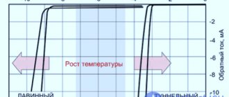
On the reverse branch of the current-voltage characteristics of the reference diode, we highlight two characteristic points 1 and 3. Point 1 corresponds to the minimum value of the stabilization current, which is within units of milliamps. If the current flowing through the zener diode is below point 1, then it will not be able to perform its functions (it will not open). If the current exceeds point 3, the reference diode will overheat and fail. Therefore, the optimal point in most cases will be the point in the middle of the reverse branch of the current-voltage characteristic, that is, point 2. Then, when the current changes within a wide range (see the Y axis), point 2 will change its position, moving up or down along the reverse branch, and the voltage will change slightly (see X axis).
Parallel parametric voltage stabilizer on zener diode
Semiconductor zener diode - (another name is Zener diode) is designed to stabilize the DC voltage of power supplies.
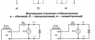
In the simplest circuit of a linear parametric stabilizer, it acts as both a source of reference voltage and a power control element. In more complex circuits, it is assigned only the role of a reference voltage source. One of the external views and designation of a zener diode:
How does a zener diode work?
The voltage to the zener diode (unlike the diode) is supplied in reverse polarity (the anode is connected to the minus and the cathode to the plus of the power source - Urev ). With this connection, reverse current flows through the zener diode - Irev . As the voltage increases, the reverse current grows very slowly (in the diagram, almost parallel to the Urev ), but at a certain voltage Urev, the zener diode junction breaks through (but destruction of the zener diode does not occur at this moment) and a reverse current of a much larger value begins to flow through it. At this moment, the current-voltage characteristic of the zener diode ( volt-voltage ) sharply goes down (almost parallel to the Irev ) - a stabilization mode begins, the main parameters of which are the minimum stabilization voltage ( Ust min ) and the minimum stabilization current ( Ist min ). With a further increase in Urev, the I-V characteristic of the zener diode again changes its direction - the stabilization mode ends, the main parameters of which are the maximum stabilization voltage ( Ust max ) and the maximum stabilization current ( Ist max ). From this moment, the zener diode loses its properties and begins to heat up, which can lead to thermal breakdown of the zener diode junction and, accordingly, to its failure.
The stabilization mode of a zener diode can be within wide limits, therefore, the documentation for zener diodes indicates the permissible minimum and maximum values of currents ( Ist min and Ist max ) and stabilization voltages ( Ust min and Ust max ). Within these ranges lie the nominal values - Ist and Ust . The rated stabilization current is usually set by manufacturers at 25%-35% of the maximum, and the rated value of the stabilization voltage is the average of the maximum and minimum.
For example, you can use the program “TBFEdit” - a reference book on radio components” and see with your own eyes what characteristics are given in the reference books on zener diodes:
For example, a Zener diode D814G: - rated stabilization current (Ist) = 5 mA; – nominal stabilization voltage (Ust) = (from 10 to 12 volts) = 11 volts; – maximum stabilization current (Ist max) = 29 mA. We will need this data when calculating the simplest voltage stabilizer.
If you could not find the required native, Soviet, zener diode, then you can use, for example, the program, Color And Code , to select a bourgeois analogue according to the required parameters:
As you can see, the D814G zener diode can easily be replaced with an analogue - BZX55C11 (which has even slightly better characteristics)
Well, now let's look at a parallel parametric voltage stabilizer using a zener diode .
A parallel parametric voltage stabilizer on a zener diode is used in low-current devices (several milliamps) and is a voltage divider (on resistor R - a ballast resistor and zener diode VD - which acts as a second resistor) to the input of which an unstable voltage is supplied and the output voltage is removed from the lower arm of the divider . As the input voltage increases (decreases), the internal resistance of the zener diode decreases (increases), which allows the output voltage to be maintained at a given level. The difference between the input supply voltage and the stabilization voltage of the zener diode drops across the ballast resistor.
Let's consider the circuit of this (the simplest) voltage stabilizer:
How to calculate the parameters of such a stabilizer. The first and most important thing to remember:
For normal operation of the circuit, the current through the zener diode must be several times (3-10 times) higher than the current in the stabilized load. In practice, since the rated stabilization current of the zener diode is several times less than the maximum, it is allowed to assume in calculations that the load current should not exceed the rated stabilization current. For example : the current consumed by the load is 10 mA, which means we need to select a zener diode such that its rated stabilization current is not less than 10 mA (it is better, of course, if it is higher).
Calculation of a parallel parametric voltage stabilizer using a zener diode
Given: Uin - input voltage = 15 volts Uout - output voltage (stabilization voltage) = 11 volts
Calculation: 1. Using the reference book given above, we determine that the D814G zener diode is suitable for our purposes: Ust (10-12V) = 11 volts Ist max = 29 mA Ist nominal = 5 mA Based on the above, we determine that the load current is not must exceed Ist - 5 mA 2. We determine the drop voltage across the ballast resistor (R) as the difference between the input and output stabilized voltage: Ufall = Uin - Uout = 15-11 = 4 volts 3. Using Ohm's law, we determine the nominal value of the ballast resistance R, dividing the drop voltage Udrop by Ist of the zener diode: R= Udrop/Ist = 4/0.005= 800 Ohm Since there are no resistors with a nominal value of 800 Ohms, we take the nearest higher value - R=1000 Ohm= 1 kOhm 4. Determine the power of the ballast resistor R : Pres= Up*Ist = 4*0.005= 0.02 watt Since not only the stabilization current of the zener diode flows through the resistor, but also the current consumed by the load, we increase the resulting value by at least 2 times: Pres = 0.004*2= 0.008 watt, which corresponds to the nearest nominal value = 0.125 watts.
What to do if you haven’t found a zener diode with the required stabilization voltage. In this case, you can use a series connection of zener diodes . For example, if we connect two D814G zener diodes in series, the stabilization voltage will be 22 volts (11+11). If we connect D814G and D810, we get a stabilization voltage of 20 volts (11+10). Any number of series connections of zener diodes of the same series is allowed (as in the example - D8**). Series connection of zener diodes of different series is allowed only if the operating currents of the series chain fall within the certified stabilization current ranges of each series used.
What to do if, in the above example, the load current is, for example, not 5 but 25 mA? You can, of course, leave everything as it is, since the maximum stabilization current (Ist max) of the D814G is 29 mA, the only thing you have to do is recalculate the power of the ballast resistor. But in this case, the zener diode will work at the limit of its capabilities and you will not have any guarantees that it will not fail. But what if the load current is, for example, 50 mA?
Back-to-back, parallel, series connection of zener diodes
To increase the stabilization voltage, two or more zener diodes can be connected in series. For example, you need to get 17 V at the load, then, if the required rating is not available, support diodes of 5.1 V and 12 V are used.
Parallel connection is used to increase current and power.
Zener diodes are also used to stabilize alternating voltage. In this case, they are connected in series and counter.
During one half-cycle of alternating voltage, one zener diode operates, and the second operates like a regular diode. In the second half-cycle, semiconductor elements perform opposite functions. However, in this case, the shape of the output voltage will be different from the input voltage and will look like a trapezoid. Due to the fact that the reference diode will cut off a voltage exceeding the stabilization level, the tops of the sine wave will be cut off.
Let's summarize:
- Zener diodes are designed to operate in reverse bias mode, providing a relatively low, stable breakdown level, that is, the stabilization voltage at which they begin to conduct significant reverse current.
- A zener diode can work as a voltage regulator, acting as an auxiliary load, drawing more current from the source if its voltage is too high, or less current if the voltage is too low.
Original article:
- Zener Diodes
Marking of zener diodes
Markings are applied to the zener diode housing in the form of numbers and letters (or letters). There are fundamentally two different types of markings. The zener diode in a glass case has the usual markings for us, directly indicating the rated stabilization voltage. The numbers can be separated by the letter V, which acts as a decimal point. For example, 5V1 means 5.1 V.
A less clear way of marking consists of four numbers and a letter at the end. If you are not an experienced radio amateur, then you can’t do without a datasheet. For example, let's decipher the parameters of the reference diode of the 1N5349B series. We are most interested in the first column, which shows the rated voltage of 12 V. The second column is the rated current value - 100 mA.
The cathode of a zener diode of any type is indicated by a black or blue ring, which is applied to the body from the side of the corresponding terminal.
Operation of the stabilizer circuit
Electrical devices that are not sensitive to small changes in supply voltage can use a conventional power supply. And more capricious devices will no longer be able to work without a stable power supply, and may simply burn out. Therefore, there is a need for an auxiliary output voltage equalization circuit.
Let's consider the operation diagram of a simple stabilizer that equalizes DC voltage using a transistor and a zener diode, which plays the role of the main element, determines, and equalizes the voltage at the output of the power supply.
Let's move on to a specific consideration of the electrical circuit of a conventional stabilizer for equalizing DC voltage.
- There is a step-down transformer with a variable output voltage of 12V.
- This voltage is supplied to the input of the circuit, and more specifically, to the diode rectifier bridge, as well as a filter made on a capacitor.
- The rectifier, made on the basis of a diode bridge, converts alternating current into direct current, but an abrupt voltage is obtained.
- Semiconductor diodes must operate at the highest current with a reserve of 25%. This current can be generated by the power supply.
- The reverse voltage should not drop less than the output voltage.
- The capacitor, which plays the role of a kind of filter, evens out these power fluctuations, converting the voltage waveform into an almost ideal graph shape. The capacitance of the capacitor should be in the range of 1-10 thousand microfarads. The voltage must also be higher than the input value.
We must not forget about the following effect: after the electrolytic capacitor (filter) and the diode rectifier bridge, the alternating voltage increases by about 18%. This means that the result is not 12 V at the output, but about 14.5 V.
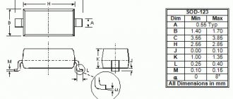
Marking of SMD zener diodes
The most widely used reference diodes are in a glass case and in a plastic case with three terminals. The SMD marking of a zener diode in a glass case consists of a colored ring, the color of which indicates the parameters of this semiconductor device.
If you come across an SMD zener diode with three terminals, then you should know that one terminal is a “dummy”, that is, it is not used and is used only for securely fixing the element on the printed circuit board after soldering. The anode and cathode of such an instance are most easily determined using a multimeter.
Zener diode power dissipation
The power dissipation of a zener diode Pst characterizes its ability not to overheat above a certain temperature for a long time. The higher the Pst , the more heat the semiconductor device can dissipate. Uin and the smallest values of Rb and In are substituted into the formula below :
There are a number of standard ratings for this parameter: 0.3 W, 0.5 W, 1.3 W, 5 W, etc. The larger Pst, the larger the dimensions of the semiconductor device.
How to check zener diode
You can check the zener diode for serviceability quite simply and quickly using a simple multimeter. To do this, the multimeter should be switched to the “continuity” mode, usually indicated by a diode sign. Then, if we touch the anode with the positive probe of the multimeter, and the cathode with the negative probe, then on the display of the measuring device we will see a certain value of the voltage drop across the pn junction. Since direct voltage is applied to the semiconductor device (see the direct branch of the current-voltage characteristic), the reference diode will open.
Now, if the probes of the multimeter are swapped, thereby applying reverse voltage to the terminals of the semiconductor device (see the reverse branch of the current-voltage characteristic), then it will be locked and will not conduct current. The meter display will show a unit, indicating infinitely high resistance.
If in both cases the multimeter shows one or rings, then the zener diode is unusable.
Parametric stabilizer
The basic circuit for connecting a zener diode, which is a parametric stabilizer
, as well as the reference voltage source in other types of stabilizers is given below.
diode connection circuit
This circuit is a voltage divider consisting of a ballast resistor R1 and a zener diode VD
, in parallel with which the load resistance RN is connected. Such a voltage stabilizer ensures stabilization of the output voltage when the supply voltage UП and load current IН change.
Let's consider the principle of operation
of this scheme. An increase in voltage at the input of the stabilizer leads to an increase in the current that passes through resistor R1 and the zener diode VD. Due to its current-voltage characteristic, the voltage on the zener diode VD will practically not change, and, accordingly, the voltage on the load resistance Rн will not change either. Thus, almost the entire voltage change will be applied to resistor R1. Thus, it is quite easy to calculate the necessary parameters of the circuit.