Literature
1. Thomas Frederiksen, Intuitive IC Op Amps (National Semiconductor Technology Series, 1984).
2. Horowitz, Paul, & Hill, Winfield, The Art of Electronics (Cambridge University Press, 1989).
3. Graeme, Jerald, Optimizing Op Amp Performance (McGraw-Hill, 1997).
4. Huijsing, Johan, Operational Amplifiers-Theory and Design (Kluwer Academic Publishers, 2001).
5. Nolan, Eric, Moghimi, Reza, “Demystifying Auto-Zero Amplifiers,” Analog Dialogue (Analog Devices, Inc., May 2000).
6. Kugelstadt, Thomas, “Auto-zero amplifiers ease the design of high-precision circuits,” TI Analog Applications Journal (2005).
Obtaining technical information, ordering samples, delivery - e-mail
•••
High side current measurement
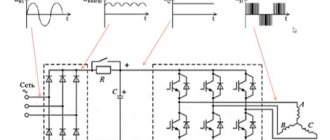
When measuring high-side current, a current shunt resistor is placed in the open circuit between the power supply and the active load (Figure 3) using a Texas Instruments INA240 as the analog front end (AFE). The common-mode input voltage of this IC can be significantly higher than the supply voltage, making it a good choice for high-side current measurements.
Rice. 3. In the high voltage side current sensing circuit, a current sensing resistor is installed between the power supply and the resistive load.
High-side current measurements have two key advantages over low-side current measurements. First, it is easy to detect a frame fault that occurs within the load because the resulting short circuit current will flow through the current shunt resistor, creating an increased voltage across it. Secondly, this measurement method is not connected to the ground point, so differential voltages on the ground bus created by large flowing currents do not affect the measurement. However, it is still recommended to place the ADC ground reference connection closer to the amplifier ground.
The high-side current measurement method has one major drawback. As noted above, it is necessary for the current amplifier to have high common mode rejection because the small voltage developed across the current shunt is only slightly lower than the load supply voltage. Depending on the system design, the common mode voltage can be quite large. The INA240 current amplifier in Figure 3 has a wide common mode voltage range from -4 to 80 volts.
17.3. Low frequency amplifiers on integrated circuits.
To build low-frequency amplifiers, ICs with the letters UN are used. Let's consider the internal circuit diagram of the K118UN1 IC, Fig. 17.1.
Rice. 17.1. Schematic diagram of IC K118UN1
Each of the two amplifier stages is made according to a common emitter circuit, and the gain can be changed by connecting an external load between pin 10 and 9 or 7; through resistors R 3
and
R 5
connecting the emitter
V 2
and the base
V 1
, interstage negative feedback is carried out inside the microcircuit. Pin 7 of the microcircuit is intended for supplying supply voltage, and pin 14 is for connecting the common wire. Pin 11 allows you to connect an external decoupling filter capacitor. Using pins 2.5 and 12, various types of feedback can be applied by connecting external elements.
By itself, this IC does not perform any of the signal processing functions, but its circuit is designed in such a way that, with a certain method of external connections (connection circuit), it ensures multifunctional use and development of amplifiers under a wide variety of technical conditions. So, for example, based on the K118UN1 IC you can assemble:
Option 1. Two-stage low-frequency amplifier (Fig. 17.2), in which both stages are made according to a circuit with a common emitter, and the gain of the second stage can be changed by connecting an external resistor R2 between pins 10 and 9.
The input (pin 3) and output (pin 10) circuits include separating capacitors C 1
and
C4
, the denominations of which are determined
by
fn .
C2
, together with the internal resistor
R 4
, constitutes an decoupling filter.
The inclusion of capacitance C3
between pins 12 and 14 (case) makes it possible to eliminate sequential current feedback in the second stage.
Rice. 17.2. Connection diagram of IC K118UN1 (option 1)
Connecting external resistor R 1
between pins 10 and 2 allows you to cover both stages of the serial OOS in voltage.
The gain of an amplifier assembled according to the circuit in Fig. 17.2 practically depends on the value of R 1
.
The larger R1 of
the OOS circuit, therefore, the gain is greater.
To limit the bandwidth on the high-frequency side,
connect
capacitance C5 with
R1 .
In this case, frequency-dependent feedback is implemented. As the frequency increases, the capacitance decreases, therefore, the depth of feedback increases, which leads to a decrease in the gain. The nominal value of capacitance C5
is calculated based on the specified upper limit frequency.
Option 2. Two-stage amplifier (Fig. 17.3), in which the first stage is made with OE
and the second - with
OK
.
Rice. 17.3. Connection diagram for IC K118UN1 (option 2)
To do this, pins 7, 9 and 10 are short-circuited through C3
on the body.
The output voltage U out
is removed from the emitter
V 2.
Connecting
C2
eliminates the serial current feedback in the first stage.
In an amplifier assembled according to the circuit in Fig. 17.3, there is a parallel feedback loop in voltage (through R 3
,
R 5
).
The same circuit simultaneously serves to bias V 1
with a fixed base current.
Option 3. Two-stage amplifier (Fig. 17.4), in which both stages are covered by serial voltage feedback (R2 and C5 between pins 2 and 10) and parallel voltage feedback (C3, C4 between pins 10 and 5). The use of various types of feedback allows you to improve the performance of the amplifier. Thus, the ULF, assembled according to the diagram in Fig. 7.4, has: f n
= 30Hz,
f in
=20 kHz,
Ko
= 100,
R in
= 50 kOhm.
Rice. 17.4. Connection diagram for IC K118UN1 (option 3)
A radio engineer, having understood the circuit diagram of an IC, can use it to develop and assemble dozens of devices with a wide variety of technical devices. But for this you need to know well the structure and circuit diagram of the IC.
To strengthen or not to strengthen?
More often than not, system designers seek to reduce the number of analog signal lines in hopes of reducing the impact of external noise. (Digital signals are generally more resistant to interference.) In the past, long analog lines required subsequent signal processing in several stages. One stage, for example, included amplification of the difference component of the signal without suppression of common-mode interference; the other, on the contrary, provided interference suppression without amplification. The use of bipolar and high-voltage power supplies in analog circuits helped improve the signal-to-noise ratio. Requirements for shorter analog line lengths and the use of low-voltage power supplies for analog circuits have spurred the evolution of amplifier architectures to address these challenges.
At the initial design stage, the question often arises: can an analog sensor and an analog-to-digital converter (ADC) work directly - i.e. without pre-processing or signal amplification. In some cases, this solution allows saving not only space on the printed circuit board, but also energy consumption. For example, high-impedance resistive bridge circuits can easily use the ADC's built-in reference voltage sources for their power supply, eliminating the need to connect an external source.
On the other hand, using an instrumentation amplifier before feeding the signal to the ADC can provide the following advantages:
- Amplifying the signal close to its source improves the overall signal-to-noise ratio in most applications, especially if the sensor is some distance from the ADC;
- The input impedance of many high-performance ADCs is relatively small, which requires the use of an amplifier with a low output impedance at the ADC input to reduce signal losses and distortion (in the absence of an amplifier, sudden changes in signal current or impedance mismatch can introduce significant distortions into the overall picture);
- An external amplifier allows you to optimize the signal, for example, using filtering;
- Using an instrumentation amplifier for the interface between the sensor and the ADC can reduce overall system cost (an unamplified signal may require a more expensive, higher resolution ADC, especially if high performance is required).
18.2. Schematic diagrams of operational amplifiers
Let's consider the circuit diagram of the operational amplifier K14OUD1A, Fig. 18.1.
Fig. 18.1. Schematic diagram of the K140UD1 operational amplifier
The input stage is made of transistors V 1
and
V 2
, a current stabilizer on transistor
V 3
with a temperature-compensating transistor
V 6
in diode connection is included in the common emitter circuit.
The output signal of the first differential stage of the op-amp is removed symmetrically from resistor R 1
and
R 2
and is fed to the second differential stage on transistors
V 4
and
V 5
.
In this cascade, a resistor R 7
, which serves to create negative feedback.
Since the output of the second differential stage is unbalanced, in the collector circuit V 4
there is no load resistance.
The output voltage is removed from resistor R 6
relative to a common point (pin 4); between these points, in addition to the amplified signal, there is a constant voltage
U k0 V 5
.
To match the potential levels of the output of the second stage and the input of the power amplifier, a DC voltage level shift circuit is used. This circuit contains a buffer emitter follower on transistor V 8
, resistor
R 9
and a current stabilizer consisting of
V 9
,
R 10
.
The output stage is built according to the emitter follower circuit on transistor V10
with load resistors
R 11
,
R 12
.
A feature of this cascade is the use of positive feedback, the elements of which include R 10
and
V 9
.
PIC allows you to obtain a gain greater than unity (about 2.5–5). Diode V 7
, operating at a reverse-biased junction, is equivalent to a small capacitor, ensuring the stability of the amplifier when covered by deep feedback.
The op-amp has two inputs: pin 9 is the inverting input, and pin 10 is the non-inverting input. The inverting input can be used to drive the output (pin 5) using external feedback voltage elements. Pins 1 and 7 are intended for supplying supply voltages, pins 2, 3 and 12 are for introducing external correction, pin 4 is a common point.