Home > Theory > RS trigger
The basic building block that makes computer memory possible, and is also used in many sequential logic devices, is the flip-flop, or bistable, circuit. Only two interconnected logic inputs constitute the basic form of this circuit, the output of which has two stable states. When the circuit is driven into any of these by a suitable input pulse, it will "remember" that state until it is changed by an additional input pulse, or until the power is turned off.
Logic chip
Classification of sequential circuits
Sequential circuits can be used for simple flip-flops or to create more complex systems: memory devices, counters, shift registers. They are divided into three main categories:
- Asynchronous, changing status when turned on;
- Synchronous, consistent with the clock signal;
- Combined, responsive to the triggering of impulses.
Important! If the circuit depends on an external input, then it is asynchronous. If the states change depending on the clock signal, then it is synchronous. To save the state, there is feedback when part of the signal from the output goes back to the input.
What is RS trigger
Cotton switch and its features
An RS flip-flop can be thought of as a one-bit memory because it retains the input pulse even after it has passed. Different types of flip-flops can be made from logic gates. The most commonly used are NAND and NOR. The most used ones are AND-NOT. This is due to their versatility, meaning that any of the other standard logic functions can be simulated.
The RS (Set-Reset) trigger circuit is one of the simplest serial connections, consisting of two cross-connected valves. The output of each is connected to the input of the other, giving a form of positive feedback.
RS trigger
The PC flip-flop has two active inputs (S and R) and two outputs (Q and Q̃ (not-Q)). For synchronous circuits, an input C with a clock signal is added.
For an RS trigger, the operating principle can be described as follows:
- Installation status. Let the input of one gate R be at logical level 0, and the input of another S be at level 1. The output of the first element Q̃ is 1 (logical NAND principle). This output is simultaneously fed to the input of the first valve. As a result, both of its inputs correspond to 1, and the output Q corresponds to 0. If the input R changes to 1, and S remains at the same level of 1, then the first gate receives another 0 input via feedback, and the output Q̃ will remain unchanged - 1. The trigger circuit is locked or set with Q equal to 0 and Q̃ equal to 1, regardless of the signal applied;
- Reset state. Is an alternative unchangeable state. Its initial conditions: the logical signal level at the input of the first gate R is 1, and the second S is 0. The output Q̃ has the value 0, Q corresponds to 1. Since one of the inputs of the second gate has logic 0, the output Q is 1 ( according to the logical AND-NOT principle). Here again the feedback works, and the first gate receives a 1 as an input. Two ones at the input provide a 0 at the output Q̃. When the given logic of the input S changes to 1 and the same signal 1 is maintained at the input R, the output Q̃ remains 0, and at Q – 1. That is, a new state is fixed, independent of changes in the input value.
Important! A signal must be supplied to the S (set) input, which puts the circuit in a state where Q is equal to one. The signal at the R (reset) input resets the circuit to the zero state.
Basics of electroacoustics
A trigger is a logical circuit with positive feedback that has two stable states - one and zero, which are designated 1 and 0, respectively (Fig. 23.1, a). At the heart of any trigger is a ring of two inverters (Fig. 23.1, b, c). A trigger is a memory element of sequential logic devices; in diagrams it is designated by the letter T
When power is applied as a result of transient processes, one of the inverters is arbitrarily set to the unit state, and the other to the zero state. Subsequently, the state of the logic elements (LE) is preserved, since the signal from the output of one LE maintains the state of the other LE. It is generally accepted to call such a circuit a memory element or latch.
Trigger inputs are divided into information and control (auxiliary). This division is largely arbitrary.
Information inputs are used to control the trigger state. Control inputs are typically used to preset a flip-flop to some state and for synchronization. As a rule, triggers have 2 outputs: direct and inverse.
Rice. 23.1. Trigger block diagram
Triggers are classified according to the method of receiving information, the principle of construction and functionality.
Based on the method of receiving information, a distinction is made between asynchronous and synchronous triggers. An asynchronous trigger changes its state immediately at the moment the corresponding information signal appears.
Synchronous triggers respond to information signals only if there is a corresponding signal at the so-called synchronization input C (from the English clock). This input is also designated by the terms “strobe”, “tact”.
Synchronous flip-flops, in turn, are divided into flip-flops with static (static) and dynamic (dynamic) control via the synchronization input C.
Static triggers perceive information signals when a logical one (direct input) or logical zero (inverse input) is applied to input C.
Dynamic triggers perceive information signals when the signal at input C changes (changes) from 0 to 1 (direct dynamic C-input) or from 1 to 0 (inverse dynamic C-input).
According to the method of construction, one- and two-stage triggers are distinguished. A single-stage trigger has one stage of storing information, and a two-stage trigger has two such stages. First, information is recorded in the first stage, and then rewritten into the second and appears at the output. A two-stage trigger is designated TT.
Based on functionality, triggers are divided into the following classes:
- — with separate setting of state 0 and 1 (RS triggers);
- — universal (JK-triggers);
- - with receiving information via one input D (D-flip-flops, or delay triggers);
- — with a counting input T (T-flip-flops).
Flip-flop inputs are usually designated as follows:
- — S – input for setting to state “1”;
- — R – input for setting to state “0”;
- — J – input for setting to state “1” in a universal trigger;
- — K – input for setting to state “0” in a universal trigger;
- — T – counting (common) input;
- — D – input for setting to state “1” or state “0”;
- — V – additional control input to allow receiving information (sometimes the letter E is used instead of V).
Let's look at some types of triggers and their implementation on logical elements.
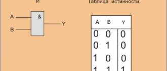
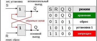
The symbolic graphical symbol of an asynchronous RS trigger and a table of its transitions are shown in Fig. 23.2.
Rice. 23.2. RS trigger
The trigger has two information inputs: S (from the English set) and R (from the English reset). It is convenient to describe the law of operation of triggers using a transition table, which is sometimes also called a truth table (Fig. 23.2). St, Rt, Qt denote the corresponding logical signals occurring at some time t, and Qt+1 the output signal at the next time t+1.
The combination of input signals St = 1, Rt = 1 is often called forbidden, since after it the trigger finds itself in a state (1 or 0), which is impossible to predict in advance. Such situations should be avoided.
The trigger in question can be implemented on two elements OR-NOT (Fig. 23.3,a) or AND-NOT (Fig. 23.3,b).
These circuits operate in full accordance with the above transition table, which is shown in Fig. 23.2 is given in abbreviated form. The complete truth table (transition table) of an RS flip-flop using NOR elements is as follows (Fig. 23.4).
Rice. 23.3. RS trigger on NOR (a) and NAND (b) elements
Rice. 23.4. Truth table of an RS flip-flop based on NOR elements
In an asynchronous RS flip-flop on NAND elements, switching is performed by a logical “0” applied to the R or S input, i.e., the inverse of the previously discussed transition table is implemented (Fig. 23.4). A prohibited combination corresponds to logical “0” at both inputs.
The K564TP2 microcircuit contains 4 asynchronous RS triggers and one control input (Fig. 23.5). When a low level is applied to the V input, the trigger outputs are disconnected from the microcircuit pins and go into the third (high-impedance) state. When a logical signal “1” is applied to input V, the flip-flops operate in accordance with the above transition table.
Rice. 23.5. RS trigger K564TP2
Consider a synchronous RS flip-flop (Fig. 23.6). If input C is logical “0”, then both the output of the upper input element “AND-NOT” and the output of the lower one will be logical “1”. And this, as noted above, ensures the storage of information. Thus, if the input C is logical “0”, then the influence on the inputs R, S does not lead to a change in the state of the trigger. If a logical one is applied to the synchronization input C, then the circuit reacts to input signals in the same way as the one discussed earlier.
In the RS flip-flops with feedback discussed above, uncertainties are possible due to the simultaneous change of information at the direct and inverse outputs associated with the R and S inputs. To eliminate this effect, two-stage triggers are used.
When using a two-stage RS trigger (Fig. 23.7), it is possible to connect its inputs and outputs. A two-stage flip-flop consists of two synchronous RS flip-flops and an additional NOT element. When input control signals and a clock signal are supplied (Fig. 23.8), information is written to the first trigger (moment t1). In this case, the second trigger does not change its state, since a logical zero is supplied to its synchronizing input from the inverter. Only after finishing writing to the first trigger when the clock signal changes from one to zero is writing to the second trigger of the two-stage system (t2).
Rice. 23.6. Synchronous RS trigger
Rice. 23.7. Block diagram of a two-stage trigger
Rice. 23.8. Timing diagram of a two-stage trigger
Thus, the two-stage flip-flop switches on the falling edge of the clock pulse. This synchronization is called dynamic. The presence of dynamic synchronization is indicated by a slash. The use of two stages in a trigger is indicated by two letters CT.
Let's consider as an example an RS flip-flop of type 136TP1 - a synchronous flip-flop. The trigger has complex inputs R and S, which cause a change in the state of the trigger when the front of the clock pulse acts (a difference from 0 to 1). Information inputs R and S have input logic “3I” (Fig. 23.9).
Inputs R and S (pins 2 and 13) – setting inputs (settings 1 and 0, respectively) operate independently whether a clock pulse is applied or not.
Rice. 23.9. Synchronous RS trigger K136TP1: a – UGO, b – truth table
The table (Fig. 23.10, b) uses the following notation:
- - any state of S, R-signals at pins 2, 13 of the IC;
- – product of signals at pins 9, 10, 11 of the IC;
- – product of signals at pins 3, 4, 5 of the IC.
Truth table
The operation of the RS trigger can be represented in the truth table:
- Q is set to logic 1 if a 0 is applied at the S input;
- Changing the S-input by one does not affect the output logic. The 0-pulse was stored by Q;
- Q is reset to 0 by a logic 0 applied to the R input;
- When R returns to 1, Q is stored at 0.
Truth table
For the conditions of the 2nd and 3rd rows of the table, Q̃ is the inverse of Q. However, in the first row, both inputs are 0, which makes Q̃ = Q = 1, and they will not be opposite logic states. In practice, this condition is not allowed, since the RS trigger loses stability.
In the last line there is a logical one at both inputs, the outputs Q̃ and Q will be in opposite states, but it is not clear what specific values they will have. They will correspond to those stored from the last input pulse.
In addition to using NAND logic, simple flip-flops can be constructed using two cross-connected AND-OR gates. The scheme works similarly. Only the disabled state will occur when both input signals are equal to one.
D – trigger
The D-flip-flop has 1 information input (D-input). There are only synchronous D-flip-flops. The state of the information input is transmitted to the output under the action of a clock pulse (input C).
D flip-flop transition table
| C | D | Q(t) | Q(t+1) | Explanations |
| * | Information storage mode | |||
| * | 1 | 1 | ||
| 1 | * | Information recording mode | ||
| 1 | 1 | * | 1 |
If input D is “1”, then upon arrival of the clock pulse Q = 1. If input D is “0”, then Q = 0.
Timing diagrams
Pulse duty cycle
Truth tables are sometimes not the best method for describing a sequential circuit. A timing diagram that shows how logic states at different points in a circuit change over time is often preferred.
RS flip-flop timing diagram
The figure shows that at the first time t1 both signals are high, which causes an uncertain state. Then from t1 to t2 S is 0, R is 1 and output Q is set to 1. There are two more undefined states: from t2 to t3 and from t4 to t5. In the interval t3-t4, the circuit is reset to 0 at output Q. And within t6-t7, the circuit is in an invalid state when R and S are equal to 0.
JK trigger
Rectifier
Other common types of logic circuits are JK, D and T, which are developments of the RS flip-flop using logic elements.
Disadvantages of the NAND-NOT RS flip-flop circuit:
- The need to avoid the condition where both input signals are 0;
- For state changes R and S that have a single input signal, the correct blocking action does not always occur.
To overcome these shortcomings, the JK flip-flop circuit was developed. Its inputs are the same R and S, but they are assigned the letters J and K after the circuit's inventor to distinguish them from other flip-flops. The JK circuit differs from the RS flip-flop in that it does not have undefined or disabled input states.
JK trigger
JK adds an input clock circuit to prevent an undefined output condition that can happen if R and S are equal to one. Therefore, there are four possible input combinations: 1, 0, “no change” and “toggle”. Input J corresponds to S, and K to R. In addition, there is a third input for each gate. The output remains Q̃ and Q.
Cross-coupling an RS flip-flop allows previously undefined flip-flop operating conditions when both inputs are 1 to be used to create a "switch" since the two inputs can be blocked.
JK circuit is SR flip- flop SET or RESET ) to be active at any time, thereby eliminating the invalid condition:
- If the SET terminal is active, the J input is blocked with status 0 (Q̃) via the lower NAND gate;
- If the RESET terminal is in effect, the K input is blocked at status 0 through the upper NAND gate.
Since Q̃ and Q are always different, they can be used to manipulate the input. For a JK flip-flop, the truth table takes the following form.
JK flip-flop truth table
When both J and K inputs are 1 at high clock, the circuit can switch from SET to RESET and vice versa.
Trigger Applications
A JK flip-flop can be thought of as a 1-bit memory cell. The supply of control signals allows you to set the memory value to 0 or 1, save or invert it, which is clearly demonstrated by the transition table.
In practice, JK devices are produced in the form of microcircuits that operate in accordance with the truth table of a synchronous flip-flop. Usually, in order to program a specific algorithm, a logical formula for converting binary signals is first compiled. Then they implement it in the form of a board, which includes the installation of triggers.
Triggers are widely used in computer system components such as counters, registers, processors, and RAM. The versatility of JK flip-flops allows them to be used in devices with different levels of operating logic complexity. For example, based on a JK trigger, you can assemble a frequency divider by 10. When pulses with a frequency of 10 kHz are received at the input of this device, the output will receive values equal to 1 kHz. Such schemes are called a decade divider or decade.
The use of JK devices as part of digital meters is their main area of application. Digital circuits in modern technology are assembled using field programmable logic chips (FPGAs) or custom chips (ASICs).
Another area of application for JK flip-flops is in devices for detecting short pulses. In this case, the pulse, after arriving at input C, goes into a single state, which is then detected by a subsequent circuit, for example, a microprocessor. The waiting multivibrator circuit also works similar to the CI detection circuit.
When creating complex logic circuits, different types of devices are needed. Therefore, it is more profitable to use a universal type of device that can operate in different modes. JK flip-flops are exactly such devices.
Synchronous circuits
It happens that it is necessary to use circuits with logical elements that operate on the basis of state changes when creating special conditions that do not depend on the status of the inputs. In this case, a logical AND component is added to the circuit, which has 2 inputs and is connected to the trigger inputs. Now the R and S inputs will be made through the AND terminal, there is also a third input for clock pulses. The change in the operation of the flip-flop is that at Q̃ and Q the state will vary due to the passage of a high clock signal at the input, called "on".
Synchronous RS flip-flop circuit
- When the clock signal is 0, the output values of the AND gates are identical, fixing the output signals in the last remembered state;
- With a clock pulse corresponding to one, the entire circuit becomes transparent and begins to work like a normal PC trigger. In this case, both inputs perceive the R and S signals.
The main advantage of a clock signal is that the output of this flip-flop can be synchronized with many other circuits and devices that use the same clock pulses. This arrangement is used for basic memory layout, for example, applying different logic states to a range of eight flip-flops, and then using a synchronous clock to cause the system to store a byte of data.
T-trigger
T flip-flops on logic gates include many of the features of previously described devices. There are models of asynchronous and synchronous types, dynamic and with an additional confirmation input.
Asynchronous
When a positive signal is received at the input, the output voltage is 2 times higher than the input. This effect is only possible with a pulse signal arriving at the T input. At the same time, the frequency of arrival on the time scale has no obstacles, which means the signal arrives much faster. Asynchronous T devices in the logical 1 state at the output have an antiphase inverted output.
Synchronous
These T flip-flops are similar to asynchronous ones. The exception is the presence of a clock signal at the input. There is also antiphase at the inverse output and the appearance of double voltage.
The design of T elements can easily be classified as pulse signal dividers. These elements only work when there is a leading edge. In other words, there is a transition from 0 to 1. But the difference lies in taking into account the time interval between pulses.
Type T flip-flops are often used in logic computing processes. This is done through the function of increasing or decreasing the voltage:
- When the output frequency increases from logical 1, a positive number is written.
- When the frequency decreases at the inverse output at logical 0, a negative number is written.
When taking into account how much memory is needed to transition and divide the signal, the element can be supplemented with an acknowledgment input. Programming using a T-flip-flop allows the device to be used in various electronic meters without built-in memory. The following is a diagram of the device's operation.