Operating principle of an electronic trigger.
The word trigger (trigger) in English means trigger. The function of a trigger is to instantly switch from one stable state to another, under the influence of an external, control factor. There are pneumatic, mechanical and relay trigger circuits. But electronic circuits, in terms of reliability and, most importantly, speed, are certainly unrivaled. The electronic trigger circuit consists of two amplification stages and, in essence, is a type of multivibrator.
The output of each stage is connected to the input of the other, but not through capacitors, as in a conventional symmetrical multivibrator, but through resistors. The values of these resistors are selected so that a cascade with a fully open transistor reliably turns off the transistor of another cascade. If you apply supply voltage to the trigger, then both cascades begin to “fight” with each other, trying to close each other.
No matter how similar the transistors are in terms of characteristics, one of them (let’s assign number 1 to it) will definitely turn out to be “stronger” and will close the other (for convenience, let’s designate it as number 2) Everything happens very quickly, it looks like transistor 1 instantly turns on, and the other (2) closed. The trigger can remain in this state for a very long time. We can call it the 1st stable state.
If you apply a voltage pulse to the input of a closed cascade (2) sufficient to open it for a short time, then when it opens it will “inhibit” cascade 1, which has been in the open state until that moment. Having closed, cascade 1 ceases to lock cascade 2, and it will remain open. Thus, the cascades will change places, the trigger will be in the 2nd stable state.
It can remain in this state for a very long time if an opening pulse is not applied to closed cascade 1. Cascade 1 opens, cascade 2 is inhibited and the trigger returns to its original state (1). It turns out that our trigger has two stable states and two control inputs, by applying pulses of sufficient amplitude to which these states can be changed.
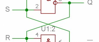
D - triggers.
To use triggers in real counting devices, it is necessary to be able to additionally control their states - presetting, resetting, activation using a counting clock pulse. To carry out this operation, three more inputs are added to the counting trigger circuit. PRESET(PR) - restores state 1 at the trigger output, and CLEAR(CL) - state 0. Using the clock input T, the trigger is generally synchronized relative to other elements of the counting device circuit. A pulse arriving at the counting input D changes the state of the trigger only if there is a 1 at the clock input.
Lesson 8.4 Triggers, registers, counters
In the previous lesson, we looked at logical elements, the state of the signal at the output of which is uniquely determined by the states of the signals at the inputs.
Logic elements serve as the basis for creating more complex digital devices, one of which is a trigger. A trigger is a whole class of electronic devices that can remain in one of two stable states for a long time after the signal that changes the state has stopped. The state of the trigger's output is determined not only by the signals at its inputs, but also by the previous state of the device. Thus, a flip-flop is the simplest one-bit memory cell.
RS trigger
The simplest trigger can be obtained from two logical elements 2OR-NOT:
Circuit designation:
This circuit is an asynchronous RS flip-flop.
It has two inputs: S (set) - installation, R (reset) - reset, and two outputs: Q (direct) and Q with an overbar (inverse, NOT_Q).
When a logical zero signal is applied to both inputs of the trigger, its outputs will be set to an arbitrary state. Let's say Q = 0 and NOT_Q =1. If a “1” is applied to input S, then the state of output Q will abruptly change to “1”, and NOT_Q will change to “0”. And this state will be maintained regardless of whether “0” or “1” is applied to the S input, which is a manifestation of the memory property.
Accordingly, when the level “1” is applied to the input R, the output Q will become “0”, and NOT_Q will become “1”.
The duration of the establishing pulses can be very short, and is limited by the physical speed of the logical modules from which the trigger is built.
The situation when the R and S inputs are high is unacceptable, since the circuit cannot operate correctly. This is a disadvantage of the RS trigger.
An RS flip-flop can also be built from two NAND elements; such elements are more common:
Installation and reset of the trigger on the 2I-NOT elements, unlike the previous one, is carried out by a low level of the input signal.
If we add two more 2I-NOT gates to the last circuit, we get a synchronous RS flip-flop.
The state of such a trigger changes only when input C (Clock) is exposed to a synchronizing (clock) pulse.
D-trigger
By slightly changing the circuit of a synchronous RS flip-flop, you can get a D flip-flop. (D-delay, delay). It has only one information input D.
If a “1” is applied to this input and then a pulse is applied to input C, then the output Q will be “1”; if a “0” is applied to the input, then a pulse is applied to C, then the output Q will be “0”. Thus, the D-flip-flop delays the information arriving at the input.
If input D is connected to output NOT_Q, then the trigger will change its state every time the state of input C changes from “0” to “1”. When changing from "1" to "0", the state of the trigger will not change. Thus, the frequency of the output pulses will be half the frequency of the input pulses. Such a flip-flop is called a counting or T-flip-flop. The frequency divider is used very widely in digital technology.
There is a type of synchronous RS flip-flop that does not have a prohibited combination - a JK flip-flop. It has three inputs: J (instead of R), K (instead of S), and C. If “1” is applied to both information inputs, then the JK flip-flop operates as a counting T flip-flop with input C.
Storage register
More complex digital devices, such as registers, can be built using flip-flops. Registers are designed to store multi-bit information, that is, numbers written in binary code.
Consider a three-bit storage register on D flip-flops:
Each flip-flop can store one digit (bit) of a number. Input R is used to set the outputs of all flip-flops to the zero (initial) state before recording a number that is supplied to inputs D0, D1 and D2. When a pulse is applied to input C, information is recorded from these inputs. Information can be stored indefinitely as long as input C is not pulsed and power is supplied.
Shift register
Another type of register is a shift register. It is designed to transform information by bitwise shifting it in one direction or another. The following figure shows a diagram of the simplest right shift register (according to the diagram):
Unlike the storage register, the output of the previous flip-flop is connected to the input of the next one. Information in the form of a logical level is supplied to the input of the first (leftmost) flip-flop. When a pulse is applied to input C, the information present at input D is written to the first flip-flop. When the second pulse is applied, the information from the first trigger is rewritten into the second trigger, and the information that is at that moment present at input D is written into the first, and so on. Thus, with each clock pulse, the information in the register shifts to the right by 1 bit.
Shift registers are used in many circuit solutions in the construction of digital devices, primarily for converting serial code into parallel, as well as for performing arithmetic operations (multiplication and division by 2) with binary numbers, organizing delay lines, generating pulses of a given duration, generating pseudo-random sequences (codes), etc.
Counter
Another class of digital devices that can be built on flip-flops are counters. As the name suggests, they count input pulses in a given code and can store the result.
The simplest sequential carry counter can be obtained using counting T-flip-flops:
By applying a pulse to input R, the counter is brought to its initial state when outputs Q1-Q3 are at a logical zero level.
Pulses for counting are supplied to input C. With the arrival of the falling edge of the first pulse, the first (left) trigger in the circuit is set to “1”. If you read the code from right to left, it corresponds to one. For our three-digit counter, this is code 001. With the arrival of the second pulse at “1,” the second trigger switches, and the first switches to “0.” Thus, the code at the counter outputs will be 010, which corresponds to the decimal digit 2. The next pulse will set the code 011, that is, 3. A three-digit counter can count up to code 111, which corresponds to the decimal digit 7. In this case, the so-called counter overflow occurs, and with the arrival of the next pulse will reset the counter to zero.
Since the counter triggers are connected in series, they will also switch in series. This process is displayed on the graph, from which it can be seen that the switching delay time tз will double and triple. As the number of bits increases, the delay may become unacceptable, which is a disadvantage of serial carry counters.
To increase performance, counters with parallel transfer are used, which is achieved by simultaneously applying input pulses to the inputs of all counter triggers. This is realized by introducing AND logic elements into the circuit:
From the diagram it can be seen that the counting pulse will arrive at the input of the second trigger only when the output of the first trigger is “1”, and to the third - when “1” is at the outputs of both the first and second triggers. Obviously, with an increase in the number of bits, it is necessary to increase both the number of logical AND elements and the number of their inputs, which, in turn, is a disadvantage of this type of counter.
Registers and counters, in turn, can be used to build more complex digital devices: adders, RAM and ROM (random access and read-only memories), ALUs (arithmetic logic units) that are part of processors, and so on, to an increasingly complex digital devices.
In the next series of articles, we'll begin our introduction to microcontrollers, a remarkable class of digital chips that are true computers that fit on a single chip and are found in most electronic devices, from coffee machines to spaceships!
Logic gates (logical elements).
The processes necessary for the functioning of any technological devices (including PCs) can be implemented using a limited set of logical elements.
Buffer.
A buffer is a current amplifier that serves to match various logic gates, especially those based on different element bases (TL or CMOS).
Inverter.
An element used to invert incoming signals - a logical one turns into zero, and vice versa.
Logic diagram I.
And is an element of logical multiplication. A one (high voltage level) at the output appears only if there are ones present at both inputs at the same time.
An example of using the AND element in a real technical device: According to technical. According to the task, the mechanical press should operate only when two buttons separated by a certain distance are pressed simultaneously. The meaning of those The task is to ensure that both hands of the operator are occupied while the press is moving, which would eliminate the possibility of accidental injury to a limb. This can be implemented just using the AND gate.
Logic circuit AND - NOT.
NAND is the most commonly used element. It consists of AND and NOT logic gates connected in series.
OR logic circuit.
OR is a logical addition circuit. A logical one at the output appears if a high level (one) is present at any of the inputs.
Logic circuit OR - NOT.
OR - NOT consists of logical elements OR and NOT connected in series. Accordingly, it does NOT invert the values at the OR output.
Exclusive OR logic circuit.
This gate produces a logical one at the output if one of the inputs is one and the other is zero. If the inputs have the same values, the output is zero.
What are triggers - briefly
The term trigger comes from the English word trigger - latch, trigger. To denote this scheme in English, the term flip-flop is more often used, which means “flapping”. This onomatopoeic name for an electronic circuit refers to its ability to almost instantly transition (“switch”) from one electrical state to another and vice versa.
The most common type of trigger is the so-called RS trigger (S and R, respectively, from the English set - installation, and reset - reset). The trigger symbol is shown in Fig. 5.6.
It has two symmetrical inputs S and R and two symmetrical outputs Q and , with the output signal Q being the logical negation of the signal . Each of the two inputs S and R can receive input signals in the form of short-term pulses ( ). The presence of a pulse at the input will be considered one, and its absence - zero. In Fig. Figure 5.7 shows an implementation of a flip-flop using NOR gates and the corresponding truth table.
| S | R | Q | |
| forbidden | |||
| 1 | 1 | ||
| 1 | 1 | ||
| 1 | 1 | bit storage | |
Let's analyze possible combinations of values of the inputs R and S of the flip-flop using its circuit and the truth table of the OR-NOT circuit (Table 5.5).
- If S=”1″, R=”0″ is applied to the trigger inputs, then (regardless of the state) “0” will appear at the Q output of the upper gate. After this, the inputs of the lower gate will have R=”0″, Q=”0″ and the output will become equal to “1”.
- In the same way, when “0” is applied to the S input and “1” to the R input, “0” will appear at the output, and “1” will appear at Q.
- If a logical “1” is applied to the R and S inputs, then the Q state does not change.
- Applying a logic “0” to both inputs R and S can lead to ambiguous results, so this combination of input signals is prohibited.
Since one trigger can remember only one digit of binary code, 8 flip-flops are needed to remember a byte, and 8 x 210 = 8192 flip-flops are needed to remember a kilobyte, respectively. Modern memory chips contain millions of triggers.