Logic elements were invented to perform logical operations and solve logical problems using electronics. They are created using diodes, transistors and combined elements (diode-transistor). This logic is called diode logic (DL), transistor logic (TL) and diode-transistor logic (DTL). Both field-effect and bipolar transistors are used. In the latter case, preference is given to npn type devices, as they are faster.
Logic element "OR"
The diagram of the “OR” logic element is shown in Figure 1 a. Each input can receive a signal in the form of some voltage (one) or its absence (zero). Voltage will appear across resistor R even if it appears on any of the diodes.
Rice. 1
Elements or can have several logical inputs. If not all inputs are used, then those inputs that are not used should be connected to ground (grounded) to avoid the appearance of extraneous signals.
Figure 1b shows the designation on the electrical circuit of the element, and 1c shows the truth table.
Composition of TTL logic microcircuits of small integration
Composition of TTL logic microcircuits of small integration
A logical element that serves as the basis for building other complex microcircuits is called a basic one. In TTL, the basic logical element is considered to be the 4-NOT element. A microcircuit containing two such logical elements in its case - 2 (4I-NOT), has in its designation the symbols LA1 (K155LA1).
In TTL series, AND–NOT logical elements are more common than others. They are produced in the form of independent microcircuits, and also serve as the basis for the construction of complex combinational and sequential microcircuits of medium and large integration. In addition to the basic element LA1, - 2 (4I-NOT), TTL produces logical elements LA2, - 8I-NOT, logical elements LA3, - 4 (2I-NOT), logical elements LA4, - 3 (3I-NOT).
To implement the OR function, several stages with phase-separating transistors are introduced into TTL logic elements, the outputs of these transistors are connected in parallel (collectors to collectors, emitters to emitters) as shown in Fig. 7.2.1.
Fig.7.2.1. 2I–2ILI–NOT microcircuit with collector and emitter terminals of the phase separating cascade, intended for connecting expanders via OR
If the input multi-emitter transistors of such microcircuits each have several AND inputs, then the result is an LR logic element circuit - AND-OR-NOT, very common in TTL (in TTL series thirteen types of AND-OR-NOT logic elements are produced).
In some types of these AND–OR–NOT microcircuits, the connection points of the collectors and emitters are connected to the terminals of the microcircuit, as shown in Fig. 7.2.1 with dotted lines, which allows you to connect additional input stages for the purpose of OR expansion. When depicting an AND-OR-NOT logic element or expanders with collector and emitter outputs, these outputs are marked with inclined crosses (see Fig. 7.2.2), in contrast to the logical outputs. At the pins of microcircuits marked with crosses, the potentials may differ from the levels specified by the requirements for logic levels.
Rice. 7.2.2. Conventional graphic symbols of the OR expander and the 2I–2OR–NOT logical element, the “non-logical” conclusions of which are marked with inclined crosses
To expand the OR input to TTL, special OR expanders are produced for four AND inputs (LD1), shown in Fig. 7.2.2 and Fig. 7.2.3, and for eight AND inputs (LD3).
Rice. 7.2.3. OR expander circuit, with collector and emitter outputs intended for connection in parallel to the collector and emitter terminals of the phase separating stage of the AND–OR–NOT logic element
By connecting the collector and emitter terminals of the phase separating stage of the 4I expander to the collector and emitter terminals of the phase separating stage of the 2I-2OR-NOT microcircuit, you can obtain a logic element (2-2-4)AND-3OR-NOT, as shown in Fig. 7.2.4.
Fig.7.2.4. Connection diagram of a four-input OR expander with the collector and emitter outputs connected in parallel to the collector and emitter terminals of the phase separating stage of a 2I-2OR-NOT logic element, creating a (2-2-4)AND-3OR-NOT logical element
An increase in the number of AND inputs (AND expansion) can be obtained by using elements from several AND–NOT circuits, using de Morgan's postulates. The same result can be obtained by connecting additional external diodes and a resistor to any of the AND inputs, as shown in Fig. 7.2.5.
Rice. 7.2.5. AND expansion circuit using additional external diodes and resistor
This connection reduces the performance and noise immunity of the microcircuit at the AND input to which the external diodes are connected. The static noise immunity of TTL microcircuits is 0.4 V. When a logical zero level is applied to one of the additional external diodes, the voltage drop across this open diode will almost completely compensate for the static noise immunity voltage, so any noise at zero at the input can lead to a false operation.
As for the speed of such a connection, the duration of the switching front from zero to one at the input of the logic element to which additional external diodes are connected increases significantly (almost by an order of magnitude). This is due to the fact that the charge of the parasitic capacitance of this input occurs not through the upper output transistor of the previous microcircuit, which has an internal resistance in the open state Ohm, but through an external resistor of 1 kOhm. If an additional resistor is taken of a smaller value, then the load on the previous microcircuit in a state of logical zero at its output may unacceptably increase.
Get text
Logic gate "AND"
The element diagram is shown in Fig. 2. If at least one of the inputs has a signal equal to zero, then current will flow through the diode. The voltage drop across the diode tends to zero, and accordingly the output will also be zero. A signal can appear at the output only if all diodes are closed, that is, there will be a signal at all inputs. Let's calculate the signal level at the device output:
Fig.2
in Fig. 2 b – designation on the diagram, c – truth table.
Exclusive OR (XOR)
| Symbol adopted in Russia (GOST) and Europe (IEC) | American Symbol (ANSI) |
The Exclusive OR element implements the logical addition operation modulo 2.
The output of the Exclusive OR element will be logical 1 if only one of the inputs is 1, in all other cases, the output will be 0.
Important addition
This article discusses two-input logic elements, which are most often used to make a robot with your own hands, but there are also elements with three or more inputs.
Logic element "NOT"
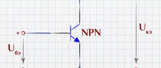
A transistor is used in the “NOT” logic element (Fig. 3 a). when there is a positive voltage at the input x=1, the transistor opens and its collector voltage tends to zero. If x = 0, then there is no positive signal at the base, the transistor is closed, the current does not pass through the collector and there is no voltage drop across the resistor R, respectively, signal E will appear on the collector. The symbol and truth table are shown in Fig. 3 b, c.
Fig.3
Power plants
Logic element "AND-NOT"
If you connect the elements “AND” and “NOT” in series according to the diagram in Fig. 2.11, then the output of the Xlogical element “AND” is inverted according to the truth table (Figure 2.12). Column X shows the output signal of the “AND” element, equal to 1 only if A = 1 and B = 1 (option 4). In turn, X is the input for the inverter. If the input X of the element is NOT logical 1, then the output Z = 0. If the input X of the element is NOT logical 0, then the output Z = 1.
Column Z shows the inverted output X of the AND gate.
In English-language literature, such a combined element is designated as NAND (short for NOT + AND).
NAND gates are used very often. They came up with their own symbol (Fig. 2.13). It comes from the AND gate symbol with a circle at the output. This circle means inverting the output. For the NAND gate, the following statement is valid:
At the output of the “AND-NOT” logic element, a logical 1 will occur only if the state 1 does not occur at all inputs.
Rice. 2.13. Symbols of “NAND” elements with two inputs
The logical function of the “AND-NOT” element corresponds to the expression:
Z = AaB.
A long bar over A and B indicates that the entire expression is inverted.
The truth table of the “AND-NOT” element is shown in Fig. 2.14.
NOR gate
Truth table of OR and NOT elements connected in series according to the diagram in Fig. 2.15 is shown in Fig. 2.16. First, input signals A and B go to the OR gate:
X= A v B.
X is also the input of the NOT element. All states of X are inverted in column Z (from X = 0 there will be Z = 1, from X = 1 there will be Z - 0).
The output Z is the output of the OR-HE gate. In English-language literature, such a combined element is designated as NOR (abbreviated from NOT + OR).
OR-HE gates are used as often as NAND gates. They also have their own symbol (Fig. 2.17). It is derived from the symbol of an OR gate with a circle at the output. This circle means inverting the output.
For an OR-HE gate, the following statement is valid:
The output of the OR-HE logic element will be logical 1 only if none of the inputs has a 1 state.
The logical function of the OR-HE element corresponds to the expression:
Z - A v B.
Rice. 2.17. Conventions for two-input NOR gates
Equivalence gate
Often there is a need for circuits in which the output is always a logical 1, when the same logical signals are applied to both inputs - either both 0 or both 1. Such a circuit is called an equivalence logic element (equivalence - equivalence). It is built from basic logical elements accordingly (Fig. 2.18).
Let us examine in detail the truth table of the equivalent element. First, for four possible combinations, the logical states of inputs A and B are recorded (Fig. 2.19, columns © and ©). Then they are inverted
element NOT, turning into A and B. If /1 = 0, then A = 1, respectively. If, as in case 4, A = 1, then A = 0, respectively. The same rule applies to B and B. This is how you get contents of columns ® and © in Fig. 2.19. The output state Q is obtained from the operation of logical multiplication of A and B. In case 1, A = 0, B = 0, therefore Q must also be equal to 0 (column ©). In cases 2 and 3, Q is also equal to 0, since both inputs are not logical 1. Only in case 4, where A = 1mB = 1, Q is also equal to 1. The symbol S in column 6 denotes the result of the logical multiplication of A and B. A and B are the inputs of the OR logic element with the output S (Fig. 2.18). In the first case, A = 1 and B = 1. Therefore, for the first case, S = 1. In cases 2 and 3, the truth tables S = 0, since only one of the inputs has a state of 1. In case 4, both inputs are 0 and, accordingly S = 0.
S and Q are the outputs of both AND elements and at the same time the inputs of the OR element. The OR gate performs the operation of logical addition of the states and Q. In case 1, Q = 0 and 1. Therefore, the output Z (column ©) is also 1. In cases 2 and 3, both inputs are 0, and thus the output is also 0. In case 4, Q = 1 and 5 = 0, which when added gives the result 1.
Equivalence elements also have their own symbol. The symbol and truth table are shown in Fig. 2.20.
The output of the equivalence element will be state 1 only when the inputs have an equal state.
The logical function of the equivalence element corresponds to the expression:
Z = (AaB)v(AaB)
Since in our example Q = A d B and
S = A l B, you can also write Z - Qv S. The equivalence element can also be constructed from other basic logical elements (see tasks at the end of Chapter 2).
Exclusive OR (XOR) gate
If the output of an equivalence element is inverted by connecting a NOT element in series, then an element appears that always has a 1 at its output if its inputs are different (Fig. 2.21).
This element is called an EXCLUSIVE OR element. We are talking about an OR element, in which the case when the output is 1 is excluded if both inputs have 1 (case 4). In English-language literature, such an element is designated as XOR (short for EXCLUSIVE + OR).
EXCLUSIVE OR logic gates are used quite often. The symbol and truth table are shown in Fig. 2.22.
The output of an EXCLUSIVE OR gate will be 1 only when both inputs have a different state.
The logical function of the equivalence element can be obtained from the circuit in Fig. 2.21:
X = (AaB)v(AaB).
Then the logical function of the EXCLUSIVE OR element can be represented as the inversion of the logical function of the equivalence element:
Z = (A l B) v (A a e)
This expression can be transformed using the rules of logical algebra:
Z = (L A B) V (D A B)
The conversion rules are discussed in detail in Chap. 4.
Rice. 2.22. Symbol of the XOR element and its truth table
Combinations of elements with two inputs
After considering the elements AND, OR, NOT, OR-HE, AND-NOT, EQUIVALENCE and EXCLUSIVE OR, let's look at the options for further possible combinations and the elements corresponding to them. There are many more connection options, but they are of little practical importance.
For elements with two inputs (for example A and B), 4 different options (combinations) of inputs are possible, as we saw in the truth tables discussed so far (see Fig. 2.22). For these 4 options, there are 4 possible output options, for example output Z in Fig. 2.23. Each of the gray squares can have an output state of 0 or 1.
Rice. 2.23. Truth table for elements with two inputs. Gray squares for possible output states.
You can create 16 different combinations of output states. They are indicated in Fig. 2.24 from Zy to Z16. It is immediately clear from the figure that some of the possible combinations are not particularly significant. For "constant 0" and "constant 1" you do not need to enter any elements. "Constant 0" means that the output is always 0, absolutely regardless of the states of the inputs. With “constant 1” the output is always 1, also regardless of the state of the inputs.
Rice. 2.24. General table for 16 possible output states of elements with two inputs
“Inversion A” and “inversion B” are respectively implemented by the NOT gate. For “identical A” and “identical B” you can use a non-inverting amplifier (Fig. 2.25).
The output of a non-inverting amplifier is only logical 1 when logical 1 is applied to the input.
Amplifiers of this kind are designed to amplify weak signals.
Inhibition is a special type of AND element. The input state is inverted before the AND element. If input A is inverted, then the element is called inhibition circuit A (Fig. 2.26). If input B is inverted, then the element is called inhibit circuit B (Fig. 2.27).
Implication is a special type of OR element. The input state is inverted before the OR gate. If input A is inverted, then the element is called implicator A (Fig. 2.28). If input B is inverted, then the element is called implicator B (Fig. 2.29).
The logical elements of prohibition and implication have limited practical value and are almost never produced. If necessary, they can be assembled from basic logical elements.
Logic elements with three or more inputs
If three or more inputs are needed, then several two-input elements can be connected in series (Fig. 2.30).
Each element with two inputs has, as is known, 4 possible combinations of inputs and outputs. For inputs A and B, the ordinary truth table is valid. If another input is added, for example C, then it can be either 0 or 1.
The previous 4 combinations from A and B are combined once with C = 0 and a second time with C = 1 (Fig. 2.31). This produces 8 combinations. If now a fourth input is added to three inputs, for example A, B, C, for example D (Fig. 2.32), then the previous 8 combinations from A, B and C are combined once with D = 0 and a second time with D = 1 (Fig. 2.33). A term with 4 inputs thus has 16 possible combinations (Figure 2.33).
With the addition of each new input, the number of combinations (input-output options) of the truth table doubles.
With two inputs - 4 combinations, with three inputs - 8 combinations, with four inputs - 16 combinations and with five inputs 32 combinations are obtained. When generating truth tables, the sequence of combinations is chosen arbitrarily. It is necessary to take into account all options and avoid repetitions. To make it easier to compile truth tables, we offer the following diagram.
The first input (for example AI) changes state every time. The second input (for example B) changes state every other time. The third input (for example C) changes state through 4 options. If we continue according to this scheme, the fourth input (for example D) changes state accordingly after 8 combinations, and so on. This scheme has proven itself in practice. The truth tables indicated in this book are compiled according to this scheme.
Currently available AND and OR gates generally have 2 to 4 inputs. The same applies to NAND and NOR gates. Rarely there are valves with 8 or more inputs.
Control test
1. Draw the symbol for AND, OR, NOT, NAND and OR-HE gates. All elements, including NOT, must have two inputs.
2. Construct the truth table of an OR gate with three inputs. The inputs are designated A, B, C. The output is designated Z
3. Suggest a variant of constructing a NAND gate from basic logical elements.
4. Draw the truth table of a NOT element with input A and output Y.
5. For the element EXCLUSIVE OR the following equation is true:
Z = (AaB)v(A*B).
Synthesize it from AND, OR and NOT gates and draw the circuit.
6. Describe in words the functions of AND and OR gates.
7. How many possible combinations does a six-input OR gate truth table have?
8. What is meant by the logical element EXCLUSIVE OR? Draw a truth table for this element.
9. What is the name of the logical element to which the truth table shown in Fig. corresponds? 2.34?
10. What function does the PROHIBITION element perform? How can it be built from basic logical elements? Draw a possible diagram.
11. Timing diagrams of inputs A and B are shown in Fig. 2.35 Draw a timing diagram for output Z if A and B are inputs
a) valve I,
b) OR gate.
Rice. 2.35. Connection of two input signals A and B
12. What logical operation is performed by the elements in the diagram in Fig. 2.36?
Rice. 2.36. Combination of logic elements.
13. Draw the truth table of a NOT gate with five inputs. Inputs are designated as Ev Ev Ev E4 and Ey Output is designated as X.
14. In Fig. Figure 2.37 shows the input signals A and B and the output signal Z of the unknown element. What logical operation does this member perform?
Rice. 2.37. Input and Output Timing Diagrams
Similar articles
Logic element "OR-NOT"
When creating various circuits using logical elements, combined elements are often used. Such elements combine several functions. The schematic diagram is shown in Fig. 4 a.
Fig.4
Here diodes D1 and D2 play the role of an “OR” element, and the transistor plays the role of an inverter. Designation of the element in the diagram and its truth table Fig. 4b and c respectively.
Add a link to a discussion of the article on the forum
RadioKot >Training >Digital technology >Basics of digital technology >
| Article tags: | Add a tag |
Logic elements
Author: Published 12/12/2005
Absolutely all digital microcircuits consist of the same logical elements - the “building blocks” of any digital node. That's what we'll talk about now.
A logic element is a circuit that has several inputs and one output. Each state of the signals at the inputs corresponds to a specific signal at the output.
So what are the elements?
Let's look:
Element “AND”
Otherwise it is called “conjunctor”.
In order to understand how it works, you need to draw a table that lists the output states for any combination of input signals. Such a table is called a " truth table ". Truth tables are widely used in digital technology to describe the operation of logic circuits.
This is what the “AND” element and its truth table look like:
Since you will have to communicate with both Russian and bourgeois tech. documentation, I will provide symbolic graphic symbols (GID) of elements both according to our and non-our standards.
We look at the truth table and clarify the principle in our brain. It is not difficult to understand: a unit at the output of the “AND” element occurs only when units are supplied to both inputs. This explains the name of the element: units must be on BOTH one AND the other input.
If we look at it a little differently, we can say this: the output of the “AND” element will be zero if zero is applied to at least one of its inputs. Let's remember. Go ahead.
OR element
In another way, he is called a “disjunctor”.
We admire:
Again, the name speaks for itself.
A unit appears at the output when a unit is applied to one OR to the other OR to both inputs at once. This element can also be called the “AND” element for negative logic: a zero at its output occurs only if zeros are supplied to both one and the second input.
Let's move on. Next we have a very simple, but very necessary element.
NOTE element
More often, it is called an “inverter”.
Do I need to say anything about his work?
Well then let's move on. The next two elements are obtained by installing an inverter at the output of the “AND” and “OR” elements.
NAND element
The NAND gate works exactly the same as the AND gate, only the output signal is completely opposite. Where the “AND” element should have a “0” output, the “AND-NOT” element should have a one. And vice versa. This is easy to understand from the equivalent circuit of the element:
Element "NOR" (NOR)
The same story - an “OR” element with an inverter at the output.
The next comrade is a little more cunning:
Exclusive OR element (XOR)
He's like this:
The operation it performs is often called "addition modulo 2". In fact, digital adders are built on these elements.
Let's look at the truth table. When is the output unit? Correct: when the inputs have different signals. On one - 1, on the other - 0. That's how cunning he is.
The equivalent circuit is something like this:
It is not necessary to memorize it.
Actually, these are the main logical elements. Absolutely any digital microcircuits are built on their basis. Even your favorite Pentium 4.
Next, we'll talk about how to synthesize a digital circuit given its truth table. This is not at all difficult, but you need to know it, because it will be useful (even useful) to us in the future.
And finally, several microcircuits containing digital elements. The numbers of the corresponding legs of the microcircuit are indicated near the terminals of the elements. All chips listed here have 14 legs. Power is supplied to legs 7 (-) and 14 (+). Supply voltage – see the table in the previous paragraph.
<<—Let’s remember what we’ve covered—Let’s move on—>>
| What do you think of this article? | Did this device work for you? | |
| 42 | 0 | 0 |
| 0 | 0 |
Logic element "AND-NOT"
The diagram is shown in Fig. 5 a. Here diode D3 acts as a filter, so to speak, to avoid signal distortion. If no signal is applied to input x1 or x2 (x1=0 or x2=0), then current will flow through diode D1 or D2. The drop across it is not zero and may be sufficient to open the transistor. The consequence may be a false positive and at the output we will get zero instead of one. And if D3 is included in the circuit, then a significant part of the voltage of the diode open at the input will drop across it, and practically nothing comes to the base of the transistor. Therefore, it will be closed, and the output will be one, which is required if there is a zero at any of the inputs. In Fig. 5b and c show the truth table and circuit designation of this device.
Fig.5
Logic elements are widely used in electronics and microprocessor technology. Many control systems are built using these devices.
Lesson 8.3 - Logic gates
8.3. Logic elements
Everything, absolutely all electronic components that process digital signals, consist of a small set of identical “building blocks”.
In low-integration microcircuits there can be units or dozens of such elements, but in modern processors there can be very, very many of them. They are called logical elements. A logical element is an electrical circuit designed to perform some logical operation with input data. Logic element is an element that implements certain logical relationships between input and output signals. The input data is represented here in the form of voltages of various levels, and the result of a logical operation at the output is also obtained in the form of a voltage of a certain level. Logic elements are usually used to construct logical circuits of computers and discrete automatic monitoring and control circuits. However, the principle of operation of digital logic remains unchanged - at the input of a logical element (there may be several inputs) there must be a digital signal (signals if there are several inputs), which uniquely determines the signal at the output of the logical element.
Of course, logical elements are built, in turn, from resistors, transistors and other electronic components already discussed in previous lessons, but from the point of view of developing digital circuits, it is the logical element that is their “elementary” particle.
When analyzing the operation of logical elements, the so-called Boolean algebra is used. The beginnings of this branch of mathematics were outlined in the works of George Boole, an English mathematician and logician of the 19th century, one of the founders of mathematical logic. The fundamentals of Boolean algebra are statements, logical operations, and functions and laws. To understand the principles of operation of logical elements, there is no need to study all the intricacies of Boolean algebra; we will master its basics in the learning process using truth tables.
A few more notes. Logic elements (as, indeed, other elements of electronic circuits) are usually designated so that the inputs are on the left and the outputs on the right. The number of inputs can, generally speaking, be anything other than zero. Real digital microcircuits can have up to 8 inputs, but we will limit ourselves to two - this is enough for understanding. Symbols correspond to domestic GOST; in other standards they may be different.
What types of logical elements are there?
Logic elements have one or more inputs and one or two (usually inverse to each other) outputs. The values of “zeros” and “ones” of the output signals of logical elements are determined by the logical function that the element performs, and the values of “zeros” and “ones” of the input signals, which play the role of independent variables. There are elementary logical functions from which any complex logical function can be composed.
The AND element , also known as a conjunctor, performs a logical multiplication operation:
Symbol - Truth Table
Here is a logical element “2I” (the number before the letter “I” means the number of inputs). The & (ampersand) sign in the upper left corner of the rectangle indicates that this is an AND gate. The first two letters of the designation DD1.2 indicate that this is a digital chip (Digital), the number to the left of the dot indicates the number of the chip on the circuit diagram, and the number to the right of the dot is the number of the logical element in this chip. One chip can contain several logic elements.
The states of the inputs in the table are designated “0” and “1” (“false” and “true”). The table shows that the output “Y” will have a state of “1” only if both inputs “X1” and “X2” are “1”. It's easy to remember: multiplying by "0" always gives "0".
The “OR” element ( OR), also known as a disjunctor, performs a logical addition operation:
Symbol - Truth Table
The output state will always be “1” as long as there is at least one “1” at the inputs.
The “NOT” element , also known as an inverter, performs the logical negation operation:
Symbol - Truth Table
The state at the input is the opposite of the state at the input.
All digital devices are built from these three elements!
Let's consider three more logical elements that can be obtained by combining those already discussed. Due to historically established circuit design solutions, these combined circuits are also considered logical elements.
Element “NAND” ( NAND), conjunct with negation:
Symbol - Truth Table
The NAND gate works exactly the same as the AND gate, only the output signal is opposite. Where the “AND” element should have a “0” output, the “AND-NOT” element will have a one. And vice versa.
Element “NOR” ( NOR), disjunctor with negation:
Symbol - Truth Table
The element works in the same way as “OR”, but with inversion of the output.
Exclusive OR element ( XOR), modulo 2 adder:
Symbol - Truth Table
In this element, there will be “1” at the output only when the inputs have different states.
Adders of binary multi-digit numbers are built on such elements. For this, another additional output is used, on which, when two “1s” appear at the inputs, a bit transfer signal appears.
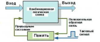
We examined logical elements that are used in digital technology to build logical circuits of any level of complexity, but the elements we examined cannot do one extremely important job - they do not know how to store information. For storage, a more complex class of devices is used, called memory elements or state machines. This class includes flip-flops, registers, counters, encoders (decoders), multiplexers (demultiplexers) and adders. We will look at some of these devices in the next lesson.
Logical foundations of computers
Any digital computer consists of logical circuits - circuits that can only be in one of two possible states - either “logical zero” or “logical one”
. Any expression, including verbal, which can be characterized as “true” and “false” can be taken as logical 0 and logical 1. In computing, logical 0 and 1 are the states of electrical circuits with certain parameters. Thus, for logic elements and circuits made using transistor-transistor logic technology (TTL circuits), logical 0 is a voltage in the range 0 ... + 0.4 V, and logical 1 is a voltage in the range + 2.4 ... + 5V []. The operation of logic circuits is described using a special mathematical apparatus called logical (Boolean) algebra or logic algebra. Boolean algebra was developed by George Boole (1815 - 1864) and is the basis of all methods for simplifying Boolean expressions.
Logical variables and logical functions are those variables and functions that can take only two values - either logical 0 or logical 1
.
Basic logical functions and elements
Logic element
— graphical representation of an elementary
logical function
.
Logical multiplication (conjunction) - AND function
Let's consider the key diagram shown in Fig. 1.1,a. Let's take logical 0 []:
- at the input of the circuit, the open
state of the corresponding switch, for example, ; - at the output of the circuit ( ) is its state when no current flows through
resistance R.
A truth table is a table containing all possible combinations of input logical variables and their corresponding logical function values.
Rice.
1.1. Three-input AND gate
Truth table for the logic circuit shown in Fig. 1.1, b, consists of 8 lines, since this circuit has three inputs - , and . Each of these logical variables can be either in the state of logical 0 or logical 1. Accordingly, the number of combinations of these variables is equal to . It is obvious that current flows through resistance R only when all three switches are closed - and , and , and . Hence, another name for logical multiplication is the AND logical element. In logical circuits, this element, regardless of the element base on which it is implemented, is designated as shown in Fig. 1.1, c.
Rule of
logical multiplication
: if at least one logical 0 is supplied to the input of a logical element AND, then its output will be logical 0.
Logic level 0 is decisive for
logical multiplication
.
In logical expressions, several variants of notation for logical multiplication are used. So, for the one shown in Fig. 1.1, in a three-input AND element, the logical expression can be represented as:
- or , but it should be clear from the context that this multiplication is logical;
- or ;
- or - using the conjunction sign;
- or , but it should be clear from the context that between the variables , and logical multiplication is performed.
Logical addition (disjunction) - OR function
Let's consider the key diagram shown in Fig. 1.2,a. Truth table
for this
logical circuit
(Fig. 1.2,b) consists of 4 lines, since this circuit has two inputs - and .
The number of combinations of these variables is equal to .
is
obvious that current flows
when
either or
is .
Hence another name for logical addition - logical OR
.
In logic circuits,
the corresponding
logical element,
regardless of the element base on which it is implemented, is designated as shown in Fig. 1.2, c.
Rice.
1.2. Two-input OR gate
Logical addition
rule : if at least one logical is supplied to the input of a logical OR element, then its output will be logical 1.
For
logical addition, the decisive level is logical 1
.
In logical expressions, two options for notation of logical addition
. So, for the given two-input OR gate, the logical expression can be represented as:
- or , but it should be clear from the context that this addition is logical;
- or - using the disjunction sign.
Logical negation (inversion) - NOT function
Let's consider the key diagram shown in Fig. 1.3,a. The truth table for this circuit (Fig. 1.3b) is the simplest and consists of only 2 lines, since it (the only one of all logical elements) has only one input - . Number of options for a single Boolean variable
equals .
It is obvious that current flows
( ) when it
is not
closed, i.e.
. Another name for this logic function
is
negation
, and the corresponding logic gate is called
an inverter
.
In logic circuits,
this element, regardless of the element base on which it is implemented, is designated as shown in Fig. 1.3, c. Since it has only one input, both the logical addition sign and the logical multiplication sign are valid in its notation.
Rice.
1.3. NOT gate
Inversion rule
: passing through the inverter, the signal changes its value to the opposite.
In logical expressions, the only option for inversion notation is used:
To the main logical elements
There are two more elements that are a combination of AND, OR and NOT elements: the AND-NOT and OR-NOT elements.
Logic function and NAND element
This function performs logical multiplication
values of the input signals and then inverts the result of this multiplication.
In logic circuits,
this element, regardless of the element base on which it is implemented, is designated as shown in Fig.
1.4,a. The truth table
is shown in Fig. 1.4, b.
Rice.
1.4. Logic element AND-NOT for three inputs
If at least one logical 0 is supplied to the input of the AND-NOT logical element, then its output will be logical 1
.
In logical expressions the following notation is used:
- or , but it should be clear from the context that this multiplication is logical;
- or ;
- or ;
- or .
Logical function and NOR gate
In logic circuits
This element, regardless of the element base on which it is implemented, is designated as shown in Fig.
1.5, a. The truth table
is shown in Fig. 1.5, b.
If at least one logical 1 is supplied to the input of the OR-NOT logical element, then its output will be logical 0
.In logical expressions the following notations are used:
- or , but it should be clear from the context that this addition is logical;
- or .
Rice. 1.5. Logic element OR-NOT for two inputs
Designing your own computer. Part 1
Introductory part. "Napoleonic plans"
Almost a year ago I had the idea to understand how a computer works and how it works. And of course, there was a great desire to create your own using elementary logic elements (to be more precise, transistors). Then I had only a small idea of its work: I knew that all digital electronics are built on logical elements (for me it was like a postulate), but I could not figure out how the program was executed, numbers were summed, why interruptions... This list The questions could go on and on, but that’s not the point now. Let us determine the characteristics of the computer being developed:
- Type of logic: binary logic
- Data bus width: 32 bits
- Address bus width: 24 bits (16,777,216 32-bit numbers can be addressed)
- Execution of basic arithmetic, logical, bitwise operations on data, as well as operations on memory cells (mov, xchg)
- Implementation of the memory allocation function (4 assembly instructions are provided)
- Processing data directly and using pointers
Software
There are many programs available for the purpose of logic circuit design. But for large-scale design and debugging, only two programs satisfied my requirements (probably my requirements are too strict):
- Logic Circuit
- Logisim
Actually requirements:
- Intuitive interface
- Creating Large Size Diagrams
- Ability to create modular circuits (circuit within a circuit)
- A variety of basic logic elements with the ability to edit their parameters
- Presence of the “RAM” and/or “ROM” element
- Ability to load a binary file into RAM\ROM and save a RAM dump into a binary file
- Availability of an extensive element base for input/output of information and debugging of circuits (buttons, constants, probes, clock generator...)
In this and all subsequent posts when publishing logic circuits, I will use Logisim due to the fact that I recently switched to Ubuntu, although the entire project was made on Logic Circuit.
Action plan
Since practice does not exist without theory, to create something you need a theoretical basis. Therefore, today in the program we will consider the following theoretical aspects:
- The key element of all digital electronics is the transistor;
- Logical elements, their types;
- Technologies for constructing electronic circuits or building logical elements on transistors;
- De Morgan's laws or how to reduce the number of gates;
The key element of all digital electronics is the transistor.
The basic element for an integrated circuit is a transistor. According to the Wikipedia definition,
transistor - a radio-electronic component made of semiconductor material that allows an input signal to control current in an electrical circuit.
Logic elements are made up of transistors. Triggers, adders, logical blocks, and counters are created from logical elements. By combining all this in the right
way, you can create your own computer (or EOM).
Logic elements, their types
Logic elements are devices designed to process information in digital form.
A logical function of any complexity can be specified using the following logical elements:
- NOT element (inverter). The output will be “1” if and only if the input
will be “0”; - Element AND (conjunction). The output will be “1” if and only if all inputs
will be “1”; - OR element (disjunction). The output will be "1" when at least one input
is "1"; - Addition element modulo 2 (exclusive OR). The output will be “1” if and only if the input will have an odd
number of “1s”; - Repeater;
- Control repeater. Used to connect multiple outputs into one output
Logic gates in Logisim:
Technologies for constructing electronic circuits or building logical elements on transistors
The original idea was to build a computer not on 7400 series chips, but on transistors. And I started searching for technologies for constructing electronic circuits. The following exist:
- Resistor-transistor logic (RTL);
- Diode-transistor logic (DTL);
- Emitter-coupled logic (ECL);
- Integral injection logic (IIL, I2L, I3L, I2L);
- CMOS (CMOS; complementary metal oxide semiconductor).
Next, I read the advantages/disadvantages for each, and among them I chose resistor-transistor logic. The choice was obvious due to the fact that this logic has design simplicity and low cost. And also for this logic there is a huge selection of bipolar SMD transistors and SMD resistors. I took the transistors BC847C npn and BC857C pnp. Having closed my eyes to all the shortcomings, I plunged into recalculation of logical elements on transistors for a whole month. I made several test circuits on a breadboard using BC547C transistors. I was pleased with the results of the theoretical and practical parts. Layout:
The last stage remains - designing a synchronous T-flip-flop circuit with 847 transistors, checking its performance and analyzing frequency characteristics. The performance test is quite simple - a logical “1” is applied to the “T” input, and clock pulses from the generator are applied to the “C” input. At the output I should receive clock pulses whose frequency is half the input. If everything works at an acceptable frequency, then the whole computer will work. I designed a circuit that consists of 4 T-flip-flops. I made a printed circuit board using the photoresist method, simply soldered it and in the end I got this beauty (the width of the tracks is 0.15mm):
I connected a 5 volt power supply to the circuit, connected a generator to the input and an oscilloscope to the output. I started testing at a frequency of 1 MHz, but the circuit did not work. Then I lowered it to 20 kHz - voila, the circuit worked correctly. By manipulating the supply voltage I was able to increase the operating frequency to 40 kHz... Alas, the circuit did not live up to my expectations. In addition, only one T flip-flop worked correctly up to 40 kHz, and all the others could not go from high to low, although the internal RS flip-flops worked correctly. I conducted some more experiments on constructing logic elements, only this time using field-effect transistors. The results were satisfactory, but some problems arose:
- High cost of the project (about $1000 for transistors only);
- The problem is getting SMD field-effect transistors in Ukraine;
- The problem is to solder 15 - 20 thousand transistors on CMOS logic, instead of 7 - 10 thousand on RTL.
For myself, I made a good conclusion
: it is better to buy 7400 series microcircuits with logic elements than to make logic elements on transistors. And to clear your conscience, when the entire circuit on microcircuits is ready, you can replace several key microcircuits with transistor circuits and connect both in turn to demonstrate that all microcircuits can be replaced with transistors
De Morgan's laws or how to reduce the number of gates
De Morgan's laws are rules that relate logical operators (disjunction and conjunction) using logical negation.
In formal logic they can be written like this: Let's consider an example of using these rules in action. Let us have the following scheme:
Using De Morgan's laws, the scheme can be converted to this:
As you can see from the truth tables, the logic of these circuits is identical. Now a little postulate
: for logical elements (except logical NOT) on CMOS logic with an inverse output (for example, logical 2I-NOT) you need two fewer transistors than for logical elements with a non-inverted output (for example, logical 2I). Then, for the first circuit you will need 18 transistors, and for the second - 12 transistors. Moreover, the second circuit will work faster due to the fact that fewer gates are used and the signal will travel an order of magnitude faster.
Future plans
In the next post I'll talk about flip-flops and we'll start designing ALUs.