Transistors are designed to solve problems of amplifying and switching electrical signals. The time of rapid development of transistors was 50–80 years of the last century. Nowadays, it should be recognized that transistors as individual components are not used so often in circuits. They are widely used only inside integrated circuits.
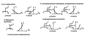
There are two types of transistors: bipolar and unipolar (field-effect).
In bipolar transistors, both electrons (negatively charged particles) and holes (positively charged particles) participate in creating currents. Hence the name of the type of transistors.
Bipolar transistors are more complex than semiconductor diodes; they have two pn junctions and three terminals called base, emitter and collector. There are two types of BT: NPN and PNP.
We will consider the device, features and circuitry using the example of NPN transistors - the most used in modern practice; for PNP transistors the reasoning is similar and the differences are only in connecting the supply voltages.
Design and principle of operation of bipolar transistors
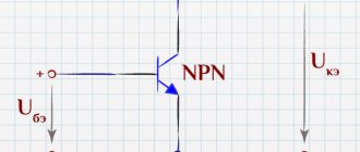
The design and operating principle of NPN transistors are shown in Figure 2.19.
An NPN transistor has three microelectronic regions: two with N-conductivity and one with P-conductivity. Each area has a pin with the names indicated in the figure.
The structure of NPN-BT can also be represented in more understandable notations: as two diodes connected by anodes in the base area.
Figure 2.20 shows the most common way of using bipolar transistors, where the base and collector are applied at positive (+) potentials relative to the emitter. In this case, the positive potential of the collector is higher than the potential of the base! In other words, the collector pn junction is reverse biased (see, the collector diode is formally closed), and the base junction is forward biased.
Moreover, if a current is set into the base, then due to the structural feature of the bipolar transistor crystal, this base current Ib will “suck” electrons from the collector region and form a collector current
Ik= β*Ib, (2.7)
where β> 1 is called the base current gain.
Typical passport values β = 20÷500. The emitter current is thus in accordance with Kirchhoff's first law
Ie = (β +1)*Ib (2.8)
Linear mode of operation of bipolar transistors
In linear mode, the bipolar transistor amplifies the input signals.
The simplest transistor circuits that can be used to amplify low voltages are shown in Figure 2.21. Circuits of this configuration are usually called circuits (cascades) with a common emitter (OE circuits), because one of the BT terminals - the emitter, is used to generate both the input and output signals - is common to them. Let us explain the operation of such an amplifier.
Let the amplified signal be an alternating sinusoidal voltage that is supplied to the input of the common emitter circuit. The amplified signal is removed from the output of the OE circuit. The amplified signal has the same sine wave shape, but is out of phase with the input signal: as the input sine wave rises, the output sine wave falls.
The main characteristic of the amplifier is the input voltage gain, which is calculated as
Kus=ΔUout/ΔUin ≈ R2/re, (2.9)
where re is the emitter resistance. The emitter resistance can be calculated using the formula:
rе= ϕт/Iе = k*T/q*Iе ≈ k*T/q*Iк, (2.10)
where k is Boltzmann’s constant,
T – temperature in kelvins,
q – electron charge.
At a temperature of +25ºС (300 K) ϕt = 26 mV.
Notes
- There is a graphical way to estimate re. This requires knowledge of the input current-voltage characteristic of the selected bipolar transistor;
- The voltage gain of the signal, as can be seen from the formula, depends on temperature. In the case where the operating range of the amplifier circuit is wide, slightly more complex modifications of the combined emitter circuit are used, which are more resistant to temperature changes.
It should be borne in mind that the expression for Kus is approximate and it will be the more valid the larger β; it is good if β >100.
Calculation of the OE circuit for direct current
At this stage, we need to calculate the values of R1 and R2, which set the direct current mode, and R2 is also included in the expression for Kus.
The operation of a bipolar transistor is described by its input and output characteristics (shown in Figure 2.22). The input characteristic Ib=ʄ(Ue), as one would expect, is similar to the characteristic of a semiconductor diode. However, for a transistor, the behavior of this characteristic also depends (slightly) on the voltage Uke. Therefore, in the technical descriptions for the selected transistor, families of input characteristics are given, where the parameter is Uke. The output characteristic is also a family of dependencies of the type Ik = ʄ (Uke), the parameter for which is the base current Ib.
Both families have fundamentally nonlinear behavior, however, this does not prevent them from being used for linear amplification. To do this, you need to build a load line on the output family, calculate the position of the operating point (PT) on it and determine the initial base current from the graph.
The load line is constructed, as before for the diode, between two similar points:
Ik=Epit/R2 and Uke=Epit. In our calculation, we set the values Epit = 15 V and Ik = Epit/R2 = 30 mA. Then R2=15/0.03 = 500 Ohm. We build a straight line and select the position of the RT - this is the middle of the linear section (shown in Figure 2.22). We will call the linear section the section of the load straight line between the saturation voltage and the cutoff voltage. The RT parameters in our example correspond to the following values (shown in Figure 2.23):
Uke.rt ≈ 7 V, Ik.rt ≈ 16 mA, Ib.rt ≈ 0.3 mA.
Next: we select from the family of input characteristics the characteristic that corresponds to the found value of Uke≈ 7.0 V, set Ib = 0.3 mA, and determine Ube≈ 0.65 V. We construct the actual section of the input load line and calculate R1 = (15- 0.65) V/ 0.3 mA = 45 kOhm.
Note – In practice, the calculation is somewhat more complicated.
Let's calculate the cascade gain at t°=25 °C.
Kus = Ie R2/ ϕt = 16 mA × 500 Ohm/ 26 mV ≈ 308.
It is important now to check whether the power dissipated on the collector does not exceed the nominal nameplate value of the selected bipolar transistor.
The calculation is carried out at the operating point: Uke.rt ×Ik.rt = 7 V × 16 mA = 112 mW. This value is constant and does not change in the input signal amplification mode, when the collector voltages and currents vary over a wide range. This is explained by the fact that the collector voltage and current change in antiphase in this circuit: when the current increases, the voltage decreases, and vice versa.
Calculation of the OE circuit for alternating current
An example of the generation of output signals from a circuit with an OE under the influence of a change in the base current is shown in Figure 2.23. Under the influence of a sinusoidally varying base current (sinusoid depicted by a dotted line), the RT shifts along the load line, first up to its maximum, and then down to its minimum.
From the figure we see that when the base current changes in the range from 0.05 to 0.55 mA with an amplitude of (0.55-0.05)/2 = 250 μA, the collector current changes in the range from approximately 3 mA to 29 mA s amplitude (29-3)/2 = 13 mA. From here we have the following value of the current gain:
Ki= 13,000/250 = 52
The collector voltage varies in the range from approximately 0.5 V to 13 V with an amplitude of (13-0.5)/2 = 6.25 V. Let us emphasize once again that the change in the collector voltage is carried out in antiphase with the change in the input (amplified) current: When the base current increases, the collector current increases and the collector voltage decreases!
So far we have not said anything about capacitors C1 and C2. These are so-called coupling capacitors. They do not transmit constant components of amplified voltages and only transmit variable ones. Their values should be large enough: the larger the capacitance values, the lower ʄn - the minimum amplified frequency. Typically these capacitors have values between 1 and 100 µF.
Switching on from source inductance
The structures of most output MOSFETs are SOIC, DPAK, TO-220, etc. - similar to each other. High temperature solder connects the base of the device to the lead frame. This connection has minimal conductivity. Also, rigid wires connect the source of the device from the outer terminal to the inner layer. Sometimes there are several rigid parallel wires coming from the source pin; die-to-leadframe connection technology is used for this (Fig. 6).
Rice. 6. Design of most lead MOSFETs using the D2PAK package as an example
The gate is connected to the external terminal by a single miniature rigid conductor. Problems arise due to the presence of inductance in the source leads. A large current flows through the drain pin, as well as reverse on/off current from the gate driver.
From a practical point of view, it is impossible to see the actual voltage at the source of the output transistor. By measuring the voltage, we will get the value only at the source terminal, but in fact the source of the transistor is connected to the voltage source through the inductance of the terminal. In absolute terms, a conductor located above a grounded conductor in free space has an inductance of 0.8 nH/mm; Thus, between the voltage source and the source of the transistor there is an inductance of the order of 3...5 nH. Large transistor packages, such as the TO220, tend to have larger source inductance values.
The source inductance has the property of resisting both when the transistor is turned on and when it is turned off. The processes that occur during shutdown are much more noticeable due to the large currents flowing through the device and the greater energy stored in the source inductance.
When the transistor turns off, the source inductance tries to maintain current in accordance with the expression V = -Ldi/dt. It follows that the polarity of the voltage across the inductor changes instantly as soon as the MOSFET interrupts the current flowing through it. Before the transistor was turned off, the voltage across the source inductance had a positive potential on the crystal and a negative potential on the transistor's lead frame. After switching off, for a short time, the potentials at the ends of the source inductance change places. A positive potential is generated at the end of the inductance connected to the lead frame. During this period, this voltage is added to the gate drive voltage.
Even though the transistor turn-off control signal takes the path of least resistance, the voltage from the source inductance adds to the low voltage from the driver, thereby creating a parasitic gate state control signal.
If this stray voltage is high enough, it can turn on the device by opposing the gate driver signal (Figure 7)
Rice. 7. Turning on the transistor by a parasitic voltage acting against the gate driver signal
To overcome problems in high-speed circuits, leadless packages are used, such as the PQFN package with copper clip technology from International Rectifier, as well as the DirectFET package. MOSFETs in these packages have minimal source inductances. In devices that require lead components, we can apply a negative turn-off voltage to the gate. If there is sufficient negative gate voltage, the parasitic pulse is not able to shift the VG potential to the threshold value.
Table 1 shows the parameters of two new MOSFETs from IR - IRF6708S and IRF6728M , which are made in small and medium-sized DirectFET packages, respectively. Their use allows you to reduce the size of the printed circuit board, as well as reduce the overall cost of the system. DirectFET packaging technology allows for minimal contact resistance and parasitic lead inductance, and also has high efficiency in heat removal from the chip due to double-sided cooling and other design features.
Table 1. Parameters of new MOSFETs from International Rectifier
| Name | VDS, V | RDS(ON)type [email protected] V, mOhm | RDS(ON) type [email protected] ,5 V, mOhm | VGS, V | QG type @ 4.5 V, nC | QG type @10 V, nC |
| IRF6728M | 30 | 1,8 | 2,8 | ± 20 | 20 | 8,7 |
| IRF6708S2 | 30 | 7,5 | 12 | ± 20 | 6,6 | 2,2 |
Earlier we mentioned the diode that is formed in the pn junction of the MOSFET between the n-drain region and the p-channel source. Like any other diode, it has a reverse recovery time (Fig. 8).
Rice. 8. Typical internal diode reverse recovery time graph
The main parameters of this diode are tRR and QRR, and the conditions under which they were measured.
When the high-side transistor in a synchronous buck converter turns off, inductance begins to discharge through the internal diode of the low-side transistor. This is a loss mode that is minimized by quickly turning on the low-side transistor. The channel of the lower side transistor opens and takes all the current to itself, the diode closes.
The MOSFET's reverse recovery current flows through the channel along with the surge current from the inductance. The total current may negatively affect the safe operating area of the device.
It may seem that the only option is to select the MOSFET with the lowest QRR and/or tRR. This is wrong.
An external diode with a lower voltage VF can be connected in parallel to the internal diode: thus, the current will flow bypassing the internal diode. MOSFETs with a built-in Schottky diode, called FETky, have an internal Schottky diode in parallel with the internal diode, which performs the same role. The forward voltage VF of a Schottky diode is much less than that of a conventional pn junction. Thus, Schottky shunts the surge current. Therefore, a fast Schottky diode is needed to reduce the QRR. For high-voltage applications for which FETkeys are not manufactured, an external Schottky diode of the required or higher voltage can be placed in parallel with the internal diode of minimal inductance.
Key operating mode of bipolar transistors
Let's look at the output characteristics of the BT. When a large current is supplied to the base (>0.3 mA), the voltage Uke decreases to its minimum value (typical value 0.2 V). They say “the transistor goes into saturation mode.”
On the other hand, if no current is supplied to the base (Ib ~ 0), then the collector current is interrupted and the voltage at the output of the cascade will be equal to the supply voltage Epi - the bipolar transistor will be in “cut-off mode”.
Actually, these two states of the BT describe the key mode of its operation: the switch (transistor) is on or off, the load is connected to the power supply or is disconnected. The simplest key circuits on BT are shown in Figure 2.24. The presented circuit diagrams show that the circuits are controlled using digital signals: logical zero (“0”) and logical one (“1”). In modern practice, such signals are most often generated by microcontrollers.
Please note that both types of BT are used in circuits with positive (+Epit) power supply and the load in both cases is located in the collector circuit of the BT. In this case: a logical unit in one of the cases (NPN transistor) closes the switch, and in the other (PNP transistor) it opens it.
Key closure condition: Ib * β >Ik.us ≈ Epit/Rload. The base current can be approximately calculated for both cases as follows: Ib = (Epit-0.6)/R1.
Knowing the supply voltage, load resistance and base current amplification factor β, R1 can be calculated using the indicated formulas.
Avalanche breakdown
The easiest way to explain an avalanche breakdown is to use a flyback converter (Fig. 9).
Rice. 9. Flyback converter circuit to demonstrate the avalanche process
Assume that the RCD network structure used to minimize voltage surges across the switching MOSFET is not in-circuit. In addition, the node between the drain of the MOSFET and the primary inductance is unblocked.
When the MOSFET is turned on, current begins to increase in the primary winding in accordance with the expression V = -Ldi/dt. When the transistor turns off, the polarity of the voltage across the coil instantly changes, adding to the B+ voltage. The coil pumps voltage back to maintain current and discharge the primary inductance.
With the drain unblocked, the VDS voltage is close to or slightly higher than the B+ voltage, in this case we observe an avalanche breakdown (Fig. 10).
Rice. 10. Limited avalanche process in the Flyback converter
Avalanche breakdown is when the voltage across the MOSFET rises quickly and then cuts off at some level above the VDS voltage (usually 110...115% of VDS). Cutoff occurs when the MOSFET's internal diode breakdown voltage limits the voltage increase. Confirmation is the flat top of the surge shape.
Avalanche breakdown occurs due to the presence of inductance. For example, a solenoid or motor experiences a similar voltage surge when the key is opened with the load unlocked.
There are many articles on the topic of avalanche breakdown, which describe in detail the methods for designing and calculating such circuits.
An important digression when comparing transistors in terms of avalanche breakdown parameters. Previously, large inductance values were used as a load to evaluate and test old transistors; significantly smaller values are used to test new transistors. These differences must be taken into account when comparing transistors in terms of avalanche breakdown parameters, since new field-effect transistors at first glance will look much worse in performance than older ones.
Checking the performance of bipolar transistors
Many multimeters allow you to measure the base current gain (β; h21) of transistors with flexible leads. Figure 2.26 shows a typical solution to this problem. A transistor is connected to a special connector, following the order indicated on the front panel. The β value appears on the display.
Notes
- NPN and PNP transistors have separate sockets for connection.
- For both types of transistors, two sockets are provided for connecting the emitter. This is due to possible design differences in the pinouts of the transistors.