Minimum source-to-gate voltage for a FET that must conduct from source to drain
Simulation result for forming an inversion (electron density) channel and achieving threshold voltage (IV) in a nanowire MOSFET. Note that the threshold voltage for this device is around 0.45V.
V threshold voltage
, usually abbreviated Vth, from a field-effect transistor (FET) - the minimum gate-to-source voltage VGS (th) is necessary to create a conductive path between the source and drain terminals. This is an important scaling factor for maintaining energy efficiency.
When referring to a junction field-effect transistor (JFET), the threshold voltage is often called the "cutoff voltage". This is somewhat confusing because pinch off
When applied to an insulated gate field effect transistor (IGFET), it refers to channel pinching which results in current saturation at high source-drain bias, even if the current is never turned off.
Unlike pinch
, period, the term
threshold voltage
is unambiguous and refers to the same concept in any field-effect transistor.
Basic principles
In n-channel enhancement mode
devices, there is no conducting channel inside the transistor, and a positive gate-source voltage is required to create it.
The positive voltage attracts free-floating electrons within the body to the gate, forming a conductive channel. But first it is necessary to attract enough electrons near the gate to counteract the dopant ions added to the FET body; this forms a region without mobile phone operators called the depletion region, and the voltage at which this occurs is the
FET
threshold voltage Further increasing the gate-to-source voltage will attract even more electrons to the gate, which can create a current-carrying path from source to drain; this process is called inversion
. The opposite is true for a p-channel "enhanced mode" MOSFET. When VGS = 0, the device is turned off and the channel is open/non-conductive. Applying a negative (-ve) gate voltage to a "enhanced mode" p-MOSFET increases the conductance of the channels turning it on.
In contrast, n-channel depletion mode
devices have a current-carrying channel that naturally exists within the transistor.
Accordingly, the term threshold voltage
does not always apply to
turning
such devices on, but is instead used to indicate the voltage level at which the channel is wide enough to allow electrons to flow freely.
This ease-of-flux threshold also applies to p-channel depletion mode
devices, in which the negative voltage from gate to body/source creates a depletion layer, pushing positively charged holes away from the gate-insulator/semiconductor interface, leaving an open carrier-free region of stationary negative ions -acceptors.
For an n-channel depletion MOSFET, a negative gate-to-source voltage, -VGS will drain (hence its name) the conducting channel with its free electrons, switching the transistor to the "OFF" position. Similarly, for a p-channel "depletion mode" MOSFET, a positive gate-to-source voltage, +VGS will deplete the channel of its free holes, driving it to the "OFF" position.
In wide planar transistors, the threshold voltage is virtually independent of the drain-source voltage and is therefore a well-defined characteristic, however in modern nanometer-sized MOSFETs it is less well-defined due to the barrier reduction caused by drainage.
Depletion region of nMOSFET enhancement mode shifted below threshold
Depletion region of enhancement mode nMOSFET biased above threshold with channel formed
In the figures, the source (left) and drain (right) are indicated by n +
to indicate heavily doped (blue) n-regions.
The depletion layer dopant is designated NA−
to indicate that the ions in the (pink) depletion layer are negatively charged and there are very few holes.
In the (red) part, the number of holes is p = NA,
making the main charge neutral.
If the gate voltage is below the threshold voltage (left figure), the "enhanced mode" transistor turns off and ideally there is no current from the drain to the source of the transistor. In fact, current is present even when the gate is biased below the threshold (subthreshold leakage) current, although it is small and varies exponentially with gate bias.
If the gate voltage is above the threshold voltage (right figure), the "boost mode" transistor is turned on due to the presence of a large number of electrons in the channel at the oxide-silicon interface, creating a low resistance channel in which charging can occur. flow from drain to source. For voltages significantly above the threshold value, this situation is called a strong inversion. The channel narrows when VD
> 0 because the voltage drop due to current in the resistive channel reduces the oxide field supporting the channel as it approaches the drain.
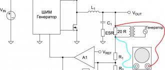
Setting up the FET Tester
Setting up the device is practically not required. A correctly assembled converter, made from serviceable parts, starts working immediately, the output voltage of 15 V is set with trimming resistor R4, monitoring the voltage with a voltmeter.
Then the sliders of resistors R1, R2 are set to the lowest position according to the diagram, which corresponds to zero voltage. Switch SA3 is moved to the 1.5 V position, and SA2 to the Uzi position. Having connected the control voltmeter to the R1 engine, move it by monitoring the reading of PA1 on the control voltmeter and if it differs, select the resistance of the resistor R3. After selecting resistor R3, switch SA3 to position 15 V and then move the R3 slider, controlling the voltage and if it also does not match, select R4. In this way, the internal voltmeter of the device is adjusted. After all the settings, close the back cover, the device is ready for use.
As practice shows, the following provisions are important for a radio amateur:
1. Check the serviceability of the PT. To do this, it is usually enough to make sure that its parameters are stable, do not “float” and are within the reference data.
2. Based on certain characteristics, select from the few PT copies available to the radio amateur those that are more suitable for use in the assembled circuit. Usually the qualitative principle of “more is less” works here.
For example, you need a field-effect transistor with a higher S or lower cutoff voltage. And from several copies, the one with the best (more or less) selected indicator is selected. Thus, high accuracy of measured parameters in practice is often not as important as one might think. Nevertheless, the proposed device makes it possible to check the performance and most important characteristics of the PT with fairly high accuracy.
Body effect
In body effect
is a change in the threshold voltage by an amount approximately equal to the change in voltage in the volume of the source, VSB { displaystyle V_{SB}} , because the body affects the threshold voltage (when it is not tied to the source).
This can be thought of as a second gate, and is sometimes called the back gate
, and accordingly the body effect is sometimes called
the back gate effect
.[1]
For an extended mode nMOS MOSFET, the volume effect at threshold voltage is calculated according to the Szychman-Hodges model,[2] which is true for older process nodes[ clarification needed
] using the following equation:
V T N = V T O + γ ( | VSB − 2 ϕ F | − | 2 ϕ F | ) { displaystyle V_{TN} = V_{TO} + gamma left ({ sqrt { left | V_ {SB} -2 phi _ {F} right |}} — { sqrt { left | 2 phi _ {F} right |}} right)}
where V T N { displaystyle V_{TN}} is the threshold voltage in the presence of bias substrate, VSB { displaystyle V_{SB)) is the displacement of the substrate from the source to the body, 2 ϕ F { displaystyle 2 phi _{F)) is the surface potential, and V T O { displaystyle V_{TO)) is the threshold voltage for zero substrate displacement, γ = ( t o X / ϵ o X ) 2 q ϵ Si N A { displaystyle gamma = left (t_{ox} / epsilon _{ox} right) { sqrt {2q epsilon _ { text {Si)) N_ {A}}}} is the body effect parameter, t o X { displaystyle t_{ox}} oxide thickness, ϵ o X { displaystyle epsilon _{bull}} oxide dielectric constant, ϵ Si { displaystyle epsilon_{ text {Si }}} is the dielectric constant of silicon, N A { displaystyle N_{A}} is the doping concentration, q { displaystyle q} is the elementary charge.
Dependence on oxide thickness
At a given process node, such as a 90 nm CMOS process, the threshold voltage depends on the choice of oxide and the thickness of the oxide
. Using the body formulas above, V T N { displaystyle V_{TN}} is directly proportional to γ { displaystyle gamma} , and T O X { displaystyle t_{OX)} , which is the oxide thickness parameter.
Thus, the thinner the oxide thickness, the lower the threshold voltage. While this may seem like an improvement, it doesn't come without a cost; because the thinner the oxide thickness, the higher the subthreshold leakage current through the device will be. Consequently, the design specification for the 90 nm gate oxide thickness was set to 1 nm to control leakage current.[3] This type of tunneling is called Fowler-Nordheim tunneling.[4]
I f n = C 1 WL ( E o x ) 2 e − E 0 E o x { displaystyle I_{fn} = C_{1} WL (E_{ox})^{2}e^{- { frac {E_ {0}}{E_{ox}}}}}
where C 1 { displaystyle C_{1)) and E 0 { displaystyle E_{0)} are constants and E o x { displaystyle E_{ox)) is the electric field through the gate oxide.
Before scaling features to 90 nm, a common solution to this problem was a dual-oxide approach to create oxide thickness. Using the 90 nm process technology, the ternary oxide approach has been adopted in some cases.[5] One standard thin oxide is used for most transistors, another for I/O driver cells, and a third for memory and pass transistor cells. These differences are based solely on the oxide thickness characteristics at the threshold voltage of CMOS technologies.
Field effect transistors. For dummies
Introduction
Now let's talk about field effect transistors. What can you assume from their name alone? Firstly, since they are transistors, they can be used to somehow control the output current. Secondly, they are supposed to have three contacts. And thirdly, their operation is based on a pn junction. What will official sources tell us about this?
Field-effect transistors
are active semiconductor devices, usually with three terminals, in which the output current is controlled using an electric field.
(electrono.ru)
The definition not only confirmed our assumptions, but also demonstrated a feature of field-effect transistors - the output current is controlled by changing the applied electric field, i.e. voltage. But for bipolar transistors, as we remember, the output current is controlled by the input base current. Another fact about field-effect transistors can be learned by paying attention to their other name - unipolar
. This means that only one type of charge carrier (either electrons or holes) is involved in the process of current flow.
The three contacts of field effect transistors are called source
(source of current carriers),
gate
(control electrode) and
drain
(electrode where carriers flow).
The structure seems simple and very similar to the design of a bipolar transistor. But it can be implemented in at least two ways. Therefore, a distinction is made between field-effect transistors with a control pn junction
and
with an insulated gate
.
In general, the idea of the latter appeared back in the 20s of the 20th century, long before the invention of bipolar transistors. But the level of technology made it possible to implement it only in 1960. In the 50s, a field-effect transistor with a control pn junction was first theoretically described and then implemented. And, like their bipolar “brothers,” field-effect transistors still play a huge role in electronics.
Before moving on to the story about the physics of the operation of unipolar transistors, I would like to remind you of the links where you can refresh your knowledge about the pn junction: one and two.
Field effect transistor with control pn junction
So, how does the first type of field-effect transistor work? The device is based on a semiconductor plate with (for example) p-type conductivity. At the opposite ends it has electrodes, by applying voltage to which we will receive current from source to drain. On top of this plate there is an area with the opposite type of conductivity, to which the third electrode is connected - the gate. Naturally, a pn junction occurs between the gate and the p-region below it ( channel
).
And since the n-layer is significantly adjacent to
the same channel, most of the transition region depleted of mobile charge carriers will fall on the p-layer. Accordingly, if we apply a reverse bias voltage to the junction, then when it closes, it will significantly increase the channel resistance and reduce the current between source and drain. Thus, the output current of the transistor is regulated using the voltage (electric field) of the gate.
The following analogy can be drawn: a pn junction is a dam that blocks the flow of charge carriers from source to drain. By increasing or decreasing the reverse voltage on it, we open/close the gateways on it, regulating the “water supply” (output current).
So, in working mode
field-effect transistor with a control pn junction, the voltage at the gate must be either zero (the channel is fully open) or reverse.
If the reverse voltage becomes so large that the blocking layer closes the channel, the transistor will go into cutoff mode
.
Even with zero gate voltage, there is a reverse voltage between gate and drain equal to the source-drain voltage. This is why the pn junction has such a jagged shape, widening towards the drain region.
It goes without saying that it is possible to make a transistor with an n-type channel and a p-type gate. The essence of his work will not change.
Conventional graphic images of field-effect transistors are shown in the figure ( a
- with a p-type channel,
b
- with an n-type channel). The arrow here indicates the direction from the p-layer to the n-layer.
Static characteristics of a field-effect transistor with a control pn junction
Since in operating mode the gate current is usually small or even zero, we will not consider graphs of the input characteristics of field-effect transistors. Let's go straight to the weekend or stock. By the way, they are called static because a constant voltage is applied to the gate. Those. there is no need to take into account frequency moments, transients, etc.
The output
(
drain
) is the dependence of the drain current on the source-drain voltage at a constant gate-source voltage.
The figure shows the graph on the left.
Three zones can be clearly distinguished on the graph. The first of them is the zone of sharp increase in drain current. This is the so-called "ohmic" region
. The source-drain channel behaves like a resistor whose resistance is controlled by the voltage at the transistor's gate.
The second zone is the saturation region
. It has an almost linear appearance. Here, the channel overlaps in the drain region, which increases with a further increase in the source-drain voltage. Accordingly, the channel resistance also increases, and the drain current changes very little (Ohm's law, however). It is this section of the characteristic that is used in amplification technology, since here there is the least nonlinear signal distortion and optimal values of small-signal parameters that are essential for amplification. These parameters include slope, internal resistance and gain. The meanings of all these obscure phrases will be revealed below.
The third zone of the chart is the breakout area
, whose name speaks for itself.
On the right side of the figure there is a graph of another important relationship - the drain-gate characteristic
. It shows how the drain current depends on the gate-source voltage when the voltage between the source and drain is constant. And it is its steepness that is one of the main parameters of a field-effect transistor.
Insulated gate field effect transistor
Such transistors are also often called MOS (metal-dielectric-semiconductor) or MOS (metal-oxide-semiconductor) transistors (metal-oxide-semiconductor field effect transistor, MOSFET).
In such devices, the gate is separated from the channel by a thin layer of dielectric. The physical basis of their work is the effect of changing the conductivity of the near-surface layer of a semiconductor at the interface with a dielectric under the influence of a transverse electric field. The structure of transistors of this type is as follows. There is a semiconductor substrate with p-conductivity, in which two heavily doped regions with n-conductivity (source and drain) are made. Between them lies a narrow near-surface bridge, the conductivity of which is also n-type. Above it, on the surface of the wafer, there is a thin layer of dielectric (most often made of silicon dioxide - hence, by the way, the abbreviation MOS). And on this layer the shutter is located - a thin metal film. The crystal itself is usually connected to the source, although it happens that it is connected separately. If a source-drain voltage is applied at zero gate voltage, then current will flow through the channel between them. Why not through the crystal? Because one of the pn junctions will be closed.
Now let’s apply a voltage negative relative to the source to the gate. The resulting transverse electric field will “push” electrons from the channel into the substrate. Accordingly, the channel resistance will increase and the current flowing through it will decrease. This mode, in which the output current decreases as the gate voltage increases, is called depletion mode.
.
If we apply a voltage to the gate, which will contribute to the appearance of a field that “helps” electrons “come” into the channel from the substrate, then the transistor will operate in enrichment mode
. In this case, the resistance of the channel will drop, and the current through it will increase.
The design of a transistor with an insulated gate discussed above is similar to the design with a control pn junction in that even with zero current on the gate and a non-zero source-drain voltage, there is a so-called initial drain current
.
In both cases, this is due to the fact that the channel for this current is built
into the transistor design.
That is, strictly speaking, we have just considered such a subtype of MOS transistors as transistors with a built-in channel
.
However, there is another type of field-effect transistors with an insulated gate - an induced (inverse) channel transistor
. From the name it is already clear that it differs from the previous one - its channel between the heavily doped areas of the drain and source appears only when a voltage of a certain polarity is applied to the gate.
So, we only apply voltage to the source and drain. No current will flow between them, since one of the pn junctions between them and the substrate is closed. Let's apply voltage to the gate (direct relative to the source). The resulting electric field will “pull” electrons from the heavily doped regions into the substrate in the direction of the gate. And when the gate voltage reaches a certain value in the near-surface zone, a so-called inversion
type of conductivity. Those. the electron concentration will exceed the hole concentration, and a thin n-type channel will appear between the drain and source. The transistor will begin to conduct current, the stronger the higher the gate voltage. From this design it is clear that a transistor with an induced channel can only operate when in enrichment mode. Therefore they are often found in switching devices.
The symbols for insulated gate transistors are as follows:
Here a
− with built-in n-type channel;
b
– with a built-in p-type channel;
c
– with output from the substrate;
g
– with an n-type induced channel;
d
– with an induced p-type channel;
e
- with output from the substrate.
Static characteristics of MOS transistors
The drain family and drain-gate characteristics of a transistor with a built-in channel are presented in the following figure:
The same characteristics for a transistor with an induced channel:
Exotic MIS structures
In order not to confuse the presentation, I just want to recommend links where you can read about them. First of all, this is everyone’s favorite Wikipedia, the section “Special Purpose MDP Structures”. And here is the theory and formulas: textbook on solid-state electronics, chapter 6, subchapters 6.12-6.15. Read it, it's interesting!
General parameters of field-effect transistors
- Maximum drain current
at a fixed gate-source voltage. - The maximum drain-source voltage
, after which breakdown occurs. - Internal (output) resistance
. It represents the channel resistance for alternating current (gate-source voltage is constant). - Slope of the drain-gate characteristic
. The larger it is, the “sharper” the transistor’s response to changes in gate voltage. - Input impedance
. It is determined by the resistance of the reverse-biased pn junction and usually reaches several and tens of megohms (which distinguishes field-effect transistors from their bipolar “relatives”). And among the field-effect transistors themselves, the palm belongs to devices with an insulated gate. - Gain
is the ratio of the change in source-drain voltage to the change in gate-source voltage at a constant drain current.
Connection schemes
Like a bipolar one, a field-effect transistor can be considered as a four-terminal device, in which two of the four contacts coincide. Thus, three types of switching circuits can be distinguished: with a common source, with a common gate and with a common drain. Their characteristics are very similar to common emitter, common base, and common collector circuits for bipolar transistors. Most often, a circuit with a common source
(
a
) is used, as it gives greater current and power gain.
A circuit with a common gate
(
b
) provides almost no current amplification and has a low input resistance.
Because of this, such a connection scheme has limited practical application.
A
common drain circuit
is also called
a source follower
. Its voltage gain is close to unity, the input impedance is high and the output impedance is low.
Differences between field-effect transistors and bipolar ones. Areas of use
As mentioned above, the first and main difference between these two types of transistors is that the latter are controlled by changing the current, and the former by voltage. And from this follow other advantages of field-effect transistors compared to bipolar ones:
- high input impedance for direct current and at high frequency, hence low control losses;
- high performance (due to the absence of accumulation and resorption of minor carriers);
- since the amplifying properties of field-effect transistors are due to the transfer of majority charge carriers, their upper limit of effective gain is higher than that of bipolar ones;
- high temperature stability;
- low noise level, since field-effect transistors do not use the phenomenon of injection of minority charge carriers, which makes bipolar transistors “noisy”;
- low power consumption.
However, with all this, field-effect transistors also have a drawback - they are “afraid” of static electricity, therefore, when working with them, they have particularly stringent requirements for protection from this scourge.
Where are field-effect transistors used? Yes, almost everywhere. Digital and analog integrated circuits, tracking and logical devices, energy-saving circuits, flash memory... Why, even quartz clocks and TV remote control work on field-effect transistors. They are everywhere, % habrowser
%. But now you know how they work!
List of sources:
ru.wikipedia.org dssp.petrsu.ru zpostbox.narod.ru electrono.ru radio.cybernet.name
Helpful comments:
https://habrahabr.ru/blogs/easyelectronics/133493/#comment_4435883 https://habrahabr.ru/blogs/easyelectronics/133493/#comment_4436509 https://habrahabr.ru/blogs/easyelectronics/133493/#comment_4441531
I recommend reading:
“Basics on your fingers”, author DI HALT (thanks to AlexeiKozlov for the tip)
Temperature dependence
Just as oxide thickness affects threshold voltage, temperature affects the threshold voltage of a CMOS device. Expanding the equation part into the body effect section
ϕ F = ( k T q ) ln ( N A p i ) { displaystyle phi _ {F} = left ({ frac {kT} {q)) right) ln { left ({ frac {N_{A)) { n_{i}}} right) )}}
where ϕ F { displaystyle phi _{F)) is half the contact potential, k { displaystyle k} is Boltzmann's Constant, T { displaystyle T} is the temperature, q { displaystyle q} is the elementary charge, N A { displaystyle N_{A} } is the doping parameter and n i { displaystyle n_{i}} is the substrate’s own doping parameter.
We see that the surface potential has a direct dependence on temperature. It can be seen above that the threshold voltage does not have a direct relationship, but does not depend on the effects. This change is typically between -4 mV/K and -2 mV/K depending on the doping level.[6] For a 30°C change, this results in a significant deviation from the 500mV design parameter typically used for a 90nm process node.
Calculation of the threshold voltage of the MIS structure taking into account the partial charges of mobile charge carriers
For most elements and devices based on MIS structures, one of the most important parameters is the threshold voltage [1].
Accurate calculation of this parameter is difficult due to the uncertainty of the values of the built-in charge in the dielectric and the distribution of surface states at the dielectric-semiconductor interface. Therefore, to achieve the calculated value, parameter adjustment using ion implantation is used [1]. But simultaneously with the threshold voltage, other parameters and characteristics of the structure change. Ion implantation has the most negative effect on the surface mobility of charge carriers, which decreases with increasing dose. This degrades the functionality of the elements. A decrease in mobility in an MOS transistor reduces the steepness of the transfer characteristic, the limiting operating frequency of the element, and worsens the static and dynamic characteristics. For charge-coupled devices, the loss of the information signal also increases.
Reducing the ion implantation dose is possible due to a more precise calculation of the threshold voltage value at the early stages of designing a MIS structure. To form the structure, a uniformly doped semiconductor substrate is used, so it is enough to consider a one-dimensional model.
Manufacturers of element base understand threshold voltage as the value of gate voltage at which the so-called subthreshold current appears in the MIS transistor, not exceeding a certain minimum value [2]. More universal, especially at the calculation stage, is the value of the gate voltage at which the surface potential of the semiconductor corresponds to the beginning of a strong surface inversion. At the beginning of the inversion, the surface concentrations of electrons and holes are equal: ps=ns=ni. At the onset of a strong inversion, the surface concentration of minority carriers is equal to the value of the volume concentration of majority charge carriers. Then the voltage drop Vsc across the surface space charge region (SCR) of the semiconductor should be equal to:
Vsc= (kT/q) ys = (kT/q) 2ln(λ), (1)
where k is Boltzmann’s constant; T—temperature on the Kelvin scale; q is the electron charge modulo; ys is the surface dimensionless potential, measured from the position of the Fermi level in the neutral volume; λ = p0/ni = ni/n0 is the degree (level) of doping.
The value of ys, which is determined by equality (1), specifies the beginning of the strong inversion (yinv).
Now consider the expression for calculating the threshold voltage, which is often used in various calculation methods and algorithms:
, (2)
where Vk
— contact potential difference, equal to the difference in the work function of an electron from the semiconductor and the metal;
Q
source is the charge of the POPC;
Q
t is the effective charge of surface states;
Qd
is the effective built-in charge of the dielectric.
For an ideal MIS structure, the values of Vk
,
Q
source and
Qd
are equal to zero.
Improvements in production technology have made it possible to reduce the influence of uncontrolled charges and carry out calculations using a model that takes into account only the contact potential difference. Charge Q
ist was calculated in the approximation of a sharp pn transition:
,
and using equality (1) we finally get:
, (3)
where N
is the effective concentration of ionized impurity in the semiconductor substrate, which determines the volume concentration of the main charge carriers; ε0 – dielectric constant; εs is the relative dielectric constant of the semiconductor [2–3].
For a more correct calculation of the threshold voltage, it is necessary to solve the Poisson equation taking into account the charge of mobile carriers. As a result of the first integration we have the following equality:
, (4)
and for a semiconductor in an equilibrium state: , (5)
where is the Debye length of the intrinsic semiconductor.
Sign rule for F
(
y
) the following: at , and vice versa.
From equation (4) it is obvious that the function F
(
y
) is the electric field strength in the POHC accurate to the factor
kT
/
q
. Using Gauss's theorem, we obtain an expression for calculating the surface charge density at the semiconductor-dielectric interface:
. (6)
To calculate the threshold voltage through it is necessary to set the value ys
in expressions (5–6) equal and replace in expression (2)
Q
source by .
Now let's evaluate how justified the proposed complication is. For an ideal Vk
,
Qd
and
Q
t are equal to zero. Then:
. (7)
For the calculation, we take typical values of the parameters of silicon integrated MOS transistors at a temperature of 300K: oxide thickness 20 nm, λ = 103...105 [1, 4]. The results are shown in Table 1.
Table 1
Absolute
and relative errors in threshold voltage calculation
| Doping parameter λ | , mV | , % |
| 1013 | 76 | 10,75 |
| 1015 | 5,6 | 0,34 |
For high-resistivity substrates, the calculation error is the most significant.
If in expression (2) we take into account all the factors that determine the threshold voltage of a real MIS structure, then the relative calculation error may decrease, but the absolute value will remain the same. Namely, the absolute value determines the dose of ion implantation of the channel region to adjust the value.
In addition, the value of the absolute error is commensurate with the terms of the voltage value of flat zones, which are determined by the values of Qt
,
Qd
.
This means that during experimental studies of these parameters, the results and their interpretation become unreliable. Therefore, when testing test samples, it is impossible to establish the true reason for the deviation of the calculated values from the experimental ones. The control of technological regimes of the processes of formation of MIS structures is also becoming more complicated [4]. Moreover, open CAD algorithms still use expression (2) [5]. Consequently, when using CAD for the calculation and design of MIS elements, it is advisable to “recheck” the calculations of the threshold voltage by replacing Q
source in expression (6).
Literature:
1. Rabai, Jean M., Chandraskan, Ananta, Nikolic, Borivozh. Digital integrated circuits. 2nd edition: Transl. from English — M: LLC “I. D. Williams", 2007. - 912 p.
2. https://www.elek.oglib.ru/bgl/4192/323.html
3. https://dssp.petrsu.ru/book/chapter6/part11.shtml
4. lib.yar.ru/yarcln/edoc/yarsu/pdf/190200.pdf
5. www.rodnik.ru/product/sapr/edaexpress/
Dependence on random fluctuation of impurity
Random dopant fluctuation (RDF) is a form of process variation resulting from changes in the concentration of an implanted dopant. In MOSFETs, RDF in the channel region can change the properties of the transistor, especially the threshold voltage. In newer processes, RDF has a greater effect because the total amount of alloying additions is less.[7]
Research is being done to suppress the dopant fluctuation that causes threshold voltage variation between devices undergoing the same manufacturing process.[8]
Recommendations
- Marco DeLaurenti, PhD thesis, Design and Optimization Methods for High Speed VLSI Circuits
(1999)) Archived 2014-11-10 on the Wayback Machine - NanoDotTek Report NDT14-08-2007, August 12, 2007
- Sugii, Watanabe and Sugatani. Transistor design for the 90 nm generation and beyond.
(2002) - S. M. Ze, Semiconductor Device Physics
, Second Edition, New York: Wiley and Sons, 1981, pp. 496–504. - Anil Telikepalli, Xilinx Inc, Power Considerations when Designing with 90 nm FPGAs
(2005)[1] - Veste and Eshraghian, CMOS VLSI Design Principles: A Systems Perspective
, Second Edition, (1993), p.48. ISBN 0-201-53376-6 - Assenov, A. Huang, Arbitrary threshold voltage drop and dopant-induced threshold voltage fluctuations in sub-0.1 μm MOSFETs: a study using 3D "atomistic" simulation, Electronic Devices, IEEE Transactions, 45, issue : 12
- Asenov, A. Huang, Suppression of random dopant-induced threshold voltage fluctuations in sub-0.1 μm MOSFETs with epitaxial and δ-doped channels, Electronic Devices, IEEE Transactions, 46, Issue: 8