For the correct functionality of many electrical devices, it is necessary to maintain certain operating parameters of the power supply network. If the voltage goes beyond the normal range, it is accompanied by a deterioration in efficiency. Pulse interference causes malfunctions. A current stabilizer on a field-effect transistor, the circuit of which is presented in this publication, will help correct the situation.
Powerful field-effect transistor power supply
Current stabilization principle
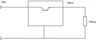
The purpose of the special circuit is to regulate the power source in automatic mode to maintain stable parameters of the load circuits. The main component is a fairly powerful semiconductor device, a current limiter at the output of the power supply.
Requirements for the control element
Selection criteria can be formulated if the current parameters (amperes) are known. However, even without a specific technical specification, it is easy to list the basic requirements:
- the current in the control circuit is maintained with a certain accuracy;
- differences in power consumption should be compensated;
- corrective changes must be made quickly enough;
- To automatically adjust the optimal mode and improve protection against interference, feedback is needed.
The essence of stabilization
To clarify the functionality of the control element, it is necessary to note the features of a typical load. The emission intensity of an LED, for example, significantly depends on the temperature during operation. The power consumption changes accordingly. As the current increases, the voltage decreases.
Important! If feedback (negative) is established, the noted change will regulate the operating mode of the control device. In particular, as the voltage between the gate and drain of the FET increases, the current through the source decreases. Thus, stabilization of the source’s output parameters is ensured without any other additional actions.
List of components
| Designation | Description | Buy on Aliexpress |
| VT1 | Powerful field effect transistor | 10pcs 2SK3919 TO-252 K3919 TO252Price: 0.98$ + 0.32$ = 1.3$ |
| VT2 | Low power transistor | 100pcs/lot BC847B SOT-23 BC847 SOT SMD 847B SOT-23Price: 0.79$ |
| R1, R2 | Resistors 1205 0.25 W (pack of 660 pcs.) | 1206 SMD Resistor Kit Assorted Kit 1ohm-1M ohm 1% 33valuesX 20pcs=660pcsPrice: 3.20$ |
| Thermally conductive adhesive Stars 922 | Star-922 Thermal Paste Thermal Grease Silicone Price: 1.54$ |
Selecting a connection scheme
Current stabilizer on a transistor
In practice, different engineering solutions are used. In particular, manufacturers offer switching power supplies to connect LED lamps. These devices perform their functions using frequency conversion and signal modulation. Microchips are installed to control the key. A throttle is used for measured energy storage.
Pulse current stabilizer
For simplicity, this article considers linear stabilization. Devices created according to this scheme do not create strong electromagnetic interference. This is the main difference from pulse analogues.
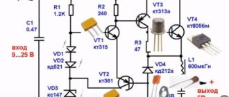
Adjustable voltage stabilizer circuit
Situations often arise when the voltage supplied by the stabilizer needs to be adjusted. The figure shows a simple circuit of an adjustable voltage and current stabilizer, which allows not only to stabilize, but also to regulate the voltage. It can be easily assembled even with only basic knowledge of electronics. For example, the input voltage is 50V, and the output is any value within 27 volts.
The main part of the stabilizer is the IRLZ24/32/44 field-effect transistor and other similar models. These transistors are equipped with three terminals - drain, source and gate. The structure of each of them consists of a dielectric metal (silicon dioxide) - a semiconductor. The housing contains a TL431 stabilizer chip, with the help of which the output electrical voltage is adjusted. The transistor itself can remain on the heatsink and be connected to the board by conductors.
This circuit can operate with input voltage in the range from 6 to 50V. The output voltage ranges from 3 to 27V and can be adjusted using a trimmer resistor. Depending on the design of the radiator, the output current reaches 10A. The capacity of smoothing capacitors C1 and C2 is 10-22 μF, and C3 is 4.7 μF. The circuit can work without them, but the quality of stabilization will be reduced. The electrolytic capacitors at the input and output are rated at approximately 50V. The power dissipated by such a stabilizer does not exceed 50 W.
Operation of current stabilizers
Transistor voltage stabilizer
The minimum number of functional elements in circuits in this category implies a reasonable cost. When choosing this option, it is not difficult to study the operating modes and configuration features.
Features of field structures
In radio devices of this type, pn junctions are located in a special way. To regulate the passage of current through the central channel, the voltage and the corresponding electromagnetic field are changed. A potential difference is created at the drain and gate.
Operating principle of field-effect and bipolar transistors
The figure shows the fundamental differences compared to a bipolar transistor. When using a field structure, there is no control current, and the input resistance becomes significantly higher. With this scheme, the device consumes a minimum of energy, but is not able to provide signal amplification. However, to solve the indicated problem (stabilization), there is no need to increase the voltage.
Transition control principle
A channel is formed in the area between p-type zones. For the passage of current, a potential difference “drain-source” is created. The transition is controlled by changing the gate-source voltage – Uzi.
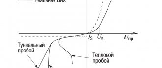
Increased stability
During operation, part of the energy is dissipated, the board and circuit components heat up, the parameters fluctuate, and most importantly, the saturation voltage (UBE) of transistor VT2 changes, the same ~0.7 V will change, which will lead to a change in the output current.
TKN ( Temperature Voltage Coefficient pn junction of the transistor is negative; with increasing temperature, UBE will decrease . For thermal stabilization, we introduce an additional element with a positive TKN - a zener diode (with Ust > 6.5 V), then when heated, the voltage on one component (VT2) will decrease, and on the other (D1) will increase, thus compensation is obtained. Ideally, the TKN of both devices should be equal in magnitude and opposite in sign, and heating should occur equally (that is why they are located next to each other on the board).
Another transistor VT3 has also been added, which acts as a current source for VT2, which will give even greater stability, because when the supply voltage changes within a certain range, the base current of VT2 will hardly change.
Design and operation of a field-effect transistor
DIY 220V voltage stabilizer circuit
To study the functionality of a field-effect transistor, you can consider two connection diagrams. In the first option, the source and gate are connected with a conductor, leveling the corresponding potential: Uzi = 0. By increasing the voltage Usi (drain-source), current flows in the working area.
Voltage is zero
In the state shown in the figure, the device functions as a typical conductor. The specific name on the graph “Ohmic region” defines the zone of proportional increase in current strength as the potential difference increases. When entering the saturation mode, the number of free charges is not enough to maintain the noted change.
Reducing gate potential
In this figure, the charge passage channel is narrowed by an additional power source, which reduces Uzi<0. At a certain level (cut-off voltage) no current flows.
Field effect transistor device
The figure shows p and n type zones. By adjusting the voltage Usi, the channel resistance (current strength) is changed. As shown above, this circuit can be closed if necessary.
Printed circuit boards
Silkscreen only: pcb_current_source_silk.pdf Tracks only: pcb_current_source_solder.pdf Tracks and silkscreen: pcb_current_source_solder_silk.pdf Silkscreen only: pcb_current_source_silk.pdf Tracks only: pcb_current_source_improved_solder.pdf Tracks and silkscreen: pcb_current_source_improved_solder_silk.pdf
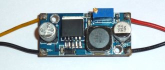
Everything fits on a small piece (3 by 2 cm) of foil PCB, heat is removed by attaching the entire board to a piece of aluminum with screws, it is designed with M2 fasteners in mind to easily and reliably fix it or simply glue it to the heat sink with heat-conducting glue (Stars 922) . If necessary, it can be easily reduced by almost half.
An example of a field-effect transistor stabilizer
When creating radio devices using lamps, a typical anode power supply does not provide the necessary stability of output parameters. Adding a resistor to the circuit increases losses and does not allow accurate adjustment of power changes in the load.
Electrical circuit of a simple stabilizer
It is not difficult to assemble this current stabilizer on a field-effect transistor with your own hands. With its help, the accuracy of the specified parameters is ensured in a range of no more than 6% of the nominal value.
Trial
The tracks were drawn with a marker, so the board is slightly different from the designed one; fastenings for the screws were not made.
We connect the device to a power source (I had a 12V transformer with a diode bridge and a capacitor), now knowing that the current is relatively small, I stupidly shorted the output with an ammeter designed to measure direct current up to 20A, the readings are below: This is an adequate result for such a circuit. Next, two 10 W LEDs with different supply voltages were connected in turn. For an LED with one crystal, the voltage output was Uout = 2.72 V at a current Iout = 0.31 A, while at the input Upit = 10.88 V, i.e. dissipates approximately:
P1 = (Upit - Uout)*Iout = (10.88-2.72)*0.31 = 8.16*0.31 = 2.53 W
For the second LED, in which three crystals are connected in series Uout = 10.32 V, Iout = 0.29 A at Upit = 11.22 V, we obtain:
P2 = (Upit - Uout)*Iout = (11.22-10.32)*0.31 = 0.9*0.31 = 0.279 W
When the input voltage differs as little as possible from the required supply voltage to provide the required current, then high efficiency is achieved (with a second LED η = 92%) with ease of implementation.
Let's replace the resistor that determines the output current of the current source with 470 Ohms, then we get the output current:
Iout = UBE/R2 = 0.6 / 471 = 1276 µA
Ammeter test:
Thus, with a 12 V power supply, we connect a 5 mm LED, a current of ~1.3 mA passes through it, through two/three LEDs the current will be the same, because the supply voltage is enough for this.
I also made a small graph of the dependence of the output stable current on the supply voltage of the current stabilizer. First, the rated current is reached (when the supply voltage is not enough for Ist), and then everything is fine, when the voltage changes three times (from 10 to 30 V), the current changes by only 0.64 mA or 4.22%.
Add a link to a discussion of the article on the forum
RadioKot >Schemes >Power supply >Power supplies >
| Article tags: | Add a tag |
Powerful laboratory power supply (LBP) 2.5…15V / 0…10A
Author: KomSoft, Published 09/08/2015 Created using KotoEd. Participant of the Competition “Congratulate the Cat as a Human Being 2015!”
Happy Birthday to Kota!!! I wish you not to grow old and receive informative articles that both young and old will enjoy reading!
Lyrical digression.
The time has come to remake my old laboratory power supply, which has served faithfully for more than 20 years. Which was successfully done according to the scheme from Eddy71. My comments and improvements are located on the pages of the corresponding forum (we will omit them for the competition). But due to the weak transformer, the output current turned out to be no more than 2A - in most cases it is enough, but sometimes more is needed.
It so happened historically that I have no reciprocity with impulse blocks. Those. Sometimes I can assemble it, repair it, and convert it from AT/ATX, but 100% results are not guaranteed. And then the transformer “430-2004” just turned up. 5 LEI-4″ from UPS with a power of 400W. On the Internet I found that “430-2004. 3 LEI-4″ core cross-section 17.15 cm2, 174 W, on both secondary windings 2x7V, resulting in 14V. Even if it’s not 400W, it’s still a lot. I decided to assemble a block on a linear stabilizer.
The paws and other thinking organs began to itch. I went online, did some digging, and selected the schemes that I liked the most. I thought about it, looked for parts, and even tried to draw a circuit board for one.
Here some nuances arose - there were missing parts, there was a board I didn’t like. Our man cannot take something ready-made - after assembly he needs to process something with a file. I’ll tell you what didn’t suit me, and at the same time I’ll remind you what’s available on the Internet.
Let's step back from the classics and move this part to the beginning, it will be clearer.
Sources of inspiration Literature:
- “12V at home or UPS “vice versa” (RadioKot > Laboratory > Analog devices, https://radiokot.ru/lab/analog/42/) is a little different.
- “A powerful laboratory power supply based on a transformer from an uninterruptible power supply” is not a laboratory at all.
- “Power supply from an uninterruptible power supply” (https://radio-house.ucoz.ru/load/istochniki_pitanija/9) - interesting, but the power transistor will get very hot, and adding a pulse step-down as in [6] will not work. The diagram was redrawn and the board layout began, but somehow it didn’t work out. And the space in the UPS case is not enough for radiators with such power dissipation. Although, in principle, I started from him.
- “Laboratory power supply 1.3-30v 0-5A” - I don’t want to work with the LM317+transistor combination (https://vrtp.ru/index.php?act=categories&CODE=article&article=81)
- “Laboratory power supply with high-speed protection” (https://www.irls.narod.ru/bp/lbp08.htm) - cool, but old (relay protection)
- “Powerful laboratory power supply” (1...15 V, 0...5A) - RadioKot > Competition: Congratulate the Cat as a human being 2013 - https://radiokot.ru/circuit/power/supply/42/. The block is very interesting, but surprisingly, parts like OP-7 (analogous to 140UD17), AP432 are in short supply, and only one KP303 was found at home. It is not clear how analogues will affect the parameters, for example, if you install TL431 instead of AP432, then the minimum output voltage will increase to 2.5-3V.
- “A simple stabilized power supply with super-affordable parts” (https://vrtp.ru/index.php?act=categories&CODE=article&article=2349), which I assembled and thoroughly studied, even modified some of it, but the current is too small, and to increase - troublesome.
- “Original Step-Down” - https://arv.radioliga.com/content/view/212/44/
- “Pulse voltage stabilizers on microcircuits and transistors” - https://radiostorage.net/?area=news/2783
- “Powerful voltage converter 24 V - 12 V with high efficiency” - https://www.diagram.com.ua/list/power/power311.shtml
I had to combine something of my own (finish it with a file). As they say: one dissertation is plagiarism, two are a compilation, three are already a dissertation.
Let's formulate the requirements:
- Voltage stabilizer from 2.5 to 15V (when changing the circuit - from 0).
- Adjustable current protection 0-10A (with stabilization or shutdown in case of overload).
- Simplicity and availability of parts (to the maximum), in the presence of a ready-made transformer. You will have to buy a powerful field worker, but if you add a pulsed step-down as in [6], you can replace it with something available from donors.
- Possibility of using pulse step-down at the input as in [6] to reduce heat generation.
What can we take from the diagrams:
- The transistor is an N-channel field effect with a current of more than 20A (because we need 10A) and a TO-247 package to improve heat dissipation (max. 180W). The TO-220 case has a max. 110W. (In the most difficult mode - at the input 16V, at the output 2.5V, a current of 10A on the control transistor will be released (16-2.5) * 10 = 135 W. With a good radiator and airflow, this may work, although it will be difficult).
- Additional (increased) power supply as in [6] and [3] - to improve stabilization and control of the N-channel field device.
- The voltage stabilizer is simpler - as in [1], [3] or [6]. For now, let's install TL431 (the lower limit will be 2.5V). If we can get AP432/TL432, we’ll reduce the lower limit to 1.25V. Or then it will be possible to do it as in [7] - then it will be from 0V, although for such currents it is not clear why this is necessary.
- Again, for simplicity, we will set the shunt to “minus” so as not to mess with the current stabilizer to obtain the reference voltage for current protection operation, as in [6].
- Let's set the regulating field switch to "plus" - in order to be able to add a pulsed step-down stabilizer to increase efficiency and reduce heating.
It is not advisable to use this block for output voltages above 15V, since a wider voltage range will complicate the circuit, and a simple radio amateur does not need such currents. And the advanced will be able to collect or purchase something more serious.
Schematic diagram of a linear stabilizer:
To avoid confusion, the final diagram obtained as a result of the experiments is given; therefore, there are gaps in the numbering of elements. For experiments up to currents of 5A, we used the IRF634 field switch that was on hand (which was later replaced by a more massive purchased one in the TO-247 IRFP250 package). Although, as we see in [6], if you have an additional pulsed step-down stabilizer, you can use something from the IRFZ30-44 series, torn from the same UPS where the transformer came from.
Why IRFP250? But because it has a constant current at 100°C - 20A (at 25°C - 33A), power dissipation - 180W, and a reasonable price - about $1.
The test subject looks like this (crocodiles hang to select current protection resistors - this is more convenient and faster than soldering individually):
Transformer connection example:
The transformer is connected through a 15A car fuse to the D50 diode bridge. The bridge must be designed for at least 15A and installed on the radiator. Connections from the transformer to the bridge, capacitor C50 and then through Jmp1, Jmp2 to the main board are made with a thick, shorter wire. To reduce heat generation, you can try to create a diode bridge from Schottky diodes, which have a lower voltage drop.
Capacitor C50 is taken at the rate of 1000 μF per 1A output current, i.e. for 10A - 10000uF. It’s better to make up several (for example, 4700 μF each) - it’s cheaper (upon purchase it turned out that 6800 μF * 25V costs 25 UAH, and 4700 * 25V - 7 UAH).
The power of the transformer allows you to make several more stabilizers with a fixed voltage (or possibly with an adjustable one). For example, they are shown in the diagram. The face of my case (from the same UPS from which the transformer is) does not allow us to normally (glamorously, while maintaining easy access) place several more output connectors, so I did not add additional stabilizers, with the exception of the “service” one on U21 to power the cooling fan.
This can be placed on a circuit board (or separate ones), or D50, C50 can be connected using a hinged installation - it depends on the design and personal preferences of each cat. For example, like this:
Description of the circuit operation.
Let's consider the operation of the unit without an additional pulse stabilizer. In this case, Jmp1 of the main board is connected to the positive of the filter output capacitor (C50), Jmp3 is connected there, Jmp2 is connected to the negative of the filter output capacitor (C50). Jmp4 and Jmp5 are connected to the input of bridge D50.
The upper part of the circuit (D10, C20, C21, U6, ...) serves to supply additional voltage to the gate of control transistor Q1. In [3], the output voltage voltmeter is also powered from it. But I have a different voltmeter, so I refused the Krenka (especially since at the plus of C22 relative to the ground - up to 42V, which, even taking into account the zener diode D11, is close to the maximum permissible for 78xx microcircuits). Replaced it with a regular parametric stabilizer.
Chain Q4-R11 is used to set a stable current of 5mA through U3 (as in [6]). With this scheme, it is enough to install a quenching resistor R18 = 1K3 with a power of 0.5 W.
If you need to simplify further, then instead of the Q4-R11 chain you can leave only the resistor R11 (see the table, calculation for the zener diode current D11 5mA).
| Current through U3, mA | R11 | R18 | |
| min. | Max. | ||
| 5 | 5 | chain Q4-R11 | 1.8K / 0.25W |
| 2 | 8 | 2.4K | 1.3K / 0.5W |
| 3 | 12 | 1.6K | 1.1K / 0.5W |
I have an smd (small) diode bridge D10, if anyone is going to assemble it using 1N4004 type diodes, it can also be simplified by removing the capacitor C20 (or C21), and instead of bridge D10 put one diode, connecting the anode to the plus of C21, and the cathode to plus C22.
Stabilizer U4 provides power to the ammeter and voltmeter. This circuit ensures the measurement of almost “pure” current (without the current consumption of the remaining elements of the circuit) and, therefore, the correct operation of the protection, but the output voltage is measured taking into account the drop across the shunt (an error of up to a maximum of 0.5V at a current of 10A and a shunt of 0.05 Ohm). I have a homemade volt and ammeter on the ICL7107, they consume about 100-120mA. The Krenka gets quite hot, I had to screw on the radiator ((20-5)V*0.2A=3W). If the voltmeter has a different common wire for power supply and measurement, even better, connect the output to points Jmp7, Jmp6 and measure the “pure” output voltage.
The top photo shows a 7805 with a radiator. During optimization, 7805 was replaced with a step-down pulse stabilizer (chopper).
Also, stabilizer U4 is used as an additional stabilization stage to obtain a reference voltage for current protection. (Note: I use U1 and U3 smd in the SOP case - that’s why the legs are numbered this way).
On the XP1 connector, the power and measuring grounds are separated, because one common wire introduced a strong error due to the current consumption of the ammeter itself (the last digit jumped quite slightly due to a change in readings and the number of included segments).
Naturally, you can use pointer voltmeters and ammeters, or you can use ready-made Chinese or any other ones - here, too, everything is up to your choice, taste, pocket and availability.
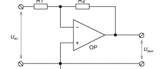
Voltage stabilization is carried out according to the standard scheme on U3. If you have a variable resistor R13 of a different value on hand (preferably at least 10K), then you can calculate the value of resistor R14 using the formula:
R14 = R13 / (Uout.max / Utl431 - 1), where Utl431 = 2.495V - TL431 reference voltage
I have R13=50K, R14=10K. Variable resistor R13 - with a linear characteristic.
Already in the process of working on the block, I learned that there is a TLV431 with a reference voltage of 1.25V. But, unfortunately, it has a maximum input (at the cathode) of 18V, so it is not applicable as U3.
Resistor R17 plays the role of a load when the unit’s output is turned off, discharging the output capacitor. Connected so that it does not affect the output current measurement.
Current protection.
Current protection is performed on op-amp U2, transistor Q2 and an additional unit. Op amp U2 compares the voltage drop across the shunt with the reference voltage taken from resistor R3. If the voltage drop across the shunt exceeds the reference voltage, the voltage at the output of U2 jumps almost to its supply voltage, which causes the transistor Q2 to turn on and the voltage at the gate of Q1 to decrease, which in turn leads to a decrease in the output voltage and, as a result, a decrease in current.
Comparators with OK (open collector) cannot be used as U2, because The flowing current is used to open the transistor and turn on the HL1 LED.
“Brakes” were noticed, namely a smooth, within 2-5 seconds, operation of the protection in the case when the current is near the threshold value, and a decrease in the stabilized current relative to the threshold after operation with a relatively large (more than 10 nF) capacitance of capacitor C9. These “brakes” are eliminated by reducing the capacitance of capacitor C9 in the feedback circuit U2 to 470 pF (but you can set it to 330 and 560).
An additional block in the simplest version for current stabilization is a resistor R15 with an LED HL1, which indicates the current stabilization mode.
In the process of creating the LBP, I went step by step, so this unit is made in the form of a separate board, which also reduces the number of connecting wires from the main board to the front panel. In principle, it can be routed on the main board by using the second half of U2. Or, if necessary, you can use the second half of U2 to amplify the signal from the shunt for the ammeter.
Additional block circuit (trigger protection):
This block allows you to switch between current stabilization modes (soft limit) and complete shutdown (hard limit).
When position SA1 is shown in the diagram, the unit operates in current stabilization mode, as described above, transferring the level from the output of the op-amp U2 to transistor Q2 through pins 2-3 of connector XP3.
When switching SA1 (locking button) to the lower position according to the circuit, voltage is supplied to base Q2 from the output of op-amp U31, turned on in comparator mode. Its response thresholds and hysteresis are set by resistors R31-R34 in such a way that it remains in a single state even after the current decreases below the threshold (voltage is removed from the input). The U30 stabilizer is designed to maintain switching thresholds. The protection is reset using the SB1 button (without fixation). When the trigger protection is triggered, the output voltage of the unit drops to zero.
Personally, in the process of assembling the previous LBP [7], it seemed more convenient to use a biscuit switch to set the operating current values instead of a variable resistor (R3), which allows you to set preset protection operating currents.
The replacement scheme is as follows:
The calculation of key elements of current protection (current limit ratings) revolves around the formula
(1) Uref * R3 / (R2+R3) = R4 * I , where
Uref is the reference voltage on 1 leg of U1, R4 is the shunt (common, i.e., in parallel with R4 and R41), I is the current through the shunt (block current).
From here we find R2 = R3 * ( Uref/(R4*Imax) - 1 )
If, instead of a variable resistor R3, a constant R3 is installed, and to reduce the protection operation current, resistors R10x are connected to it in parallel, then they can be calculated using the formula, which is obtained by simple transformations from (1):
(2) R10х = R2 / ( Uref/(I*R4) - R2/R3 - 1 )
and from here, if we designate R3p as a parallel connection of resistors R3 and R10x, we obtain the current value for real values of R10x:
(3) I = Uref * R3p / ( ( R2 + R3p ) * R4 )
A calculation (file in Excel format) that makes life easier and saves paper and pencil is attached (01.xls). Practice quite accurately agrees with theory even when using conventional MLT 10% resistors, but if desired, you can select or combine several (that’s what the crocodiles are soldered for). I used crocodiles to test the theory with practice, but I didn’t select resistors in the resulting block, I installed what was available. Therefore, in the photo at the end of the article, for example, instead of 4A, 3.9A is stabilized.
Resistor R101 with a nominal value of 390K, which is an order of magnitude larger than R3, can be omitted; there will be no visible differences. When switching the SA2 range (when its contacts are open), the maximum block current is determined by the ratio R2/R3 and at such ratings will not exceed 10A.
Example of a plate from the calculation:
Step-down switching stabilizer (replacing U4).
Due to the strong heating, the replacement 7805 was assembled according to the standard circuit for a current of 200-300mA and ripple of 1mA from what was at hand - it works great, does not heat up, does not whistle, does not harm the volt-ammeters..
Fan control.
To control the fan, a ready-made card from some kind of ATX power supply was taken. I’m giving the diagram as an example (an interesting move) - in order to unify the parts used, the developers put almost all the elements in pairs to increase power. In my diagram, the numbering is shifted by 50 relative to the original.
To prevent the fan from rotating at room temperature (while the unit is not loaded), resistor R5 (R55) is sealed off, and resistor R3 (R53) is reduced to 5K1 by selection.
When repeating, transistors Q51-Q52 can be replaced with one more powerful one (with a collector current of 0.5A), resistors R51-R52 - with one 110 Ohm with a power of 0.5W. Or use any other fan control scheme.
Details.
There were no special requirements for parts, except for the power transistor and diode bridge. For beginners, I will say that the BC817 transistor can be replaced with any of the KT503, C945 or similar series. The LM358 opamp was taken as the most common one on “donors”; there were no special requirements for it. You cannot use open collector comparators like LM393 instead. Regulating transistor - with an N-channel, a drain-source voltage of more than 40V, a 2-fold current reserve (preferably at least 15-20A) and a “the more the better” housing. The same goes for D50 rectifier diodes.
Radiators from processors were used as radiators (for the diode assembly from P3, for the regulating transistor - from P4 or higher). They are specifically designed for power dissipation of up to 100 W when blowing.
The drawing of the final printed circuit board is shown taking into account the corrections. It is better to additionally solder the power paths (and so wide) with 1mm copper wire.
Setup.
As the forum on [7] showed, the title of the article “A simple stabilized power supply with super-affordable parts” attracted a lot of novice radio amateurs who, when assembling, were unable to solve the simplest problems that were chewed over to them several times. Even searching for a faulty or unsoldered part can cause difficulties and confusion for them...
I have everything set up during the development process. But nevertheless, I will try to describe in as much detail as possible (as an example) the procedure for checking (setting up) such a block:
- Check for correct installation, absence of breaks, short circuits, etc...
- (this step is more for beginners; those who are confident can skip it) Connect the power part through an integrated stabilizer type 7818 (installed on a radiator), connecting its input to the plus of the output filter capacitor (C50), the output to point Jmp1 of the main board, common wire - to “ground” (minus the output capacitor of filter C50). This will allow you to test the unit at currents up to 1A, reducing the risk of current breakdown of the power transistor in the event of errors (internal protection 7818 will work).
- Check the presence of supply voltages on the main board (all values are given for an alternating voltage on the secondary winding of 14V), namely: +20-21V at point Jmp1 (when installing an additional 7818 - +18V), +20-21V at point Jmp3, +40 -42V on the “plus” of capacitor C22, +22V on the “plus” of capacitor C24, +5V on the “plus” of capacitor C4, +2.5V at the connection point of resistors R1 and R2.
- We connect the standard voltmeter and ammeter. (Note: In principle, you can do without an oscilloscope. If the current and voltage readings do not fluctuate, then the output is “clean”, without generation. If the voltmeter readings fluctuate, most likely there is high-frequency generation or low-frequency voltage ripples - it is advisable to check with an oscilloscope. If they fluctuate ammeter readings - most likely the measuring ground is connected incorrectly, is not separated from the power one, even changes in the indicator readings, and therefore the current consumption, lead to a change in the readings).
- We disable the current protection by disconnecting the additional board from the XP3 connector.
- By rotating resistor R13, we check the smooth change in the output voltage at the output of the block from 2.5 to 15V. The upper limit can be adjusted by selecting resistor R14 (reduce to increase the upper limit). In this case, the voltage at the gate of transistor Q1 will vary from 2.5 to (approximately) 18V. The voltage at the “plus” of C24 should remain within +21-22V and should not “sag”. If the voltage at the “plus” of C24 “sags” by more than 2V, you can reduce the resistance R18. But you shouldn’t be too zealous, because the current, and therefore the heating, of elements R18, D11, Q4, R11, U3 will increase.
- We load the block with a current of 0.5-1A. We check the same thing as in step 6 - there should be no “sags” over the entire range of output voltages. Additionally, we check the voltages as in step 3 - there should be no strong deviations. (Note: If the unit operates correctly and the voltmeter is connected in this way (and not directly to the output), when the current increases, the voltmeter readings should increase by the value Rsh*I. That is, with a shunt as in the diagram of 0.05 Ohm and a load of 1A current is connected readings increase by 0.05V, with a load of 3A - by 0.15V, 5A - by 0.25V, etc.) If a voltmeter (for example, a pointer) is connected directly to the output (to Jmp6 and Jmp7) - the readings should be stable at change in load current.
- We connect current protection by attaching an additional board to the XP3 connector. We check the presence of +12V voltage on the “plus” of C31 and 4.4V on the 2nd leg of U31A. From this point on, it is advisable to have an adjustable load or a store (set) of resistances of appropriate power.
- We set switch SA1 of the additional block to the lower (according to the diagram) position, including trigger mode (hard limitation). We set some voltage, for example 10-12V. One by one, starting from a small one, we set the limiting current and, increasing the load current, we make sure that the unit enters the protection mode. In this case, the voltage on the 7th leg of U2B jumps almost to Upit (approx. 12-20V), the HL31 LED should light up and the output voltage decreases to 0. The voltage on the 1st leg of U31B jumps to almost +12V. Briefly press SB1 - the HL31 LED will go out, the voltage will return to its original value, and the voltmeter will show the current current value. Release SB1 - the block will return to protection mode. We reduce or turn off the load - the unit should remain in protection mode. Press SB1 - the HL31 LED will go out, the voltage will return to its original value, and the voltmeter will show the current current value (zero if the load is disconnected).
- We set switch SA1 of the additional unit to the upper (according to the diagram) position, including the current stabilization mode (soft limitation). We set some voltage, for example 10-12V. One by one, starting with a small one, we set the limiting current and, increasing the load current, make sure that the unit enters the current stabilization mode. In this case, the HL31 LED should light up and the output voltage will begin to decrease at a stable current. If, after entering the current stabilization mode, the current decreases abruptly (by a small value of about 50-200 mA), you can try reducing the capacitance of C9. When the load is disconnected, HL31 should go out and the voltage should return to its original value.
- When performing steps 9-10, you can more accurately select the values of resistors R101-R111 if the protection operation current is set by a galetnik, and not by a variable resistor.
- Now you can drive the unit over the entire range of voltages up to 15V and currents up to 1A, checking all modes again. It is advisable to connect an oscilloscope and make sure that there is no high-frequency generation or low-frequency ripple at the output, especially at maximum current or voltage, or in current stabilization mode.
- If step 2 was followed (the power section was connected through an integrated stabilizer type 7818), then turn it off by connecting Jmp1 of the main board to the plus of the output filter capacitor (C50). Current protection must naturally be connected and already checked.
- We repeat the check according to points 6-7, 9-10, 12 for the entire range of voltages and currents.
Photos of the device.
The main stabilizer with a step-down module instead of 78xx for powering volt-ampere meters and a powerful power transistor (IRFP250):
Layout of the unit in a UPS housing:
The face of the block and it itself operate on an electronic load of 12V/4A (limit current - 6A). In the background you can see the culprit [7], which gives 0-30V and only 2A...:
And in defense (limit 4A is set):
The second stage is to attach the additional Step-down pulse stabilizer.
To reduce heat generation and increase the efficiency of the unit, you can use a pulsed step-down, similar to [6], which provides a voltage at the input of the control transistor that is only a few volts higher than the output.
M-yes! Easier said than done! This part took me more than six months, mainly due to lack of time. But according to the principle “any paper must be aged”, it has been successfully defeated.
I initially tinkered (for other purposes) with the Original Step-Down [8]. I really liked the synchronous rectification and low heating of the transistors. True, I was not able to squeeze more than 5-6A out of it using the recommended yellow-white ring from the ATX unit.
I overcame the current limitation by taking a core from the main transformer of the ATX power supply. The standard size turned out to be ER35/20/11, the material is presumably N87 Epcos. The chopper throttle was calculated using the Booster 5100 program for the following parameters:
- input voltage: 18-21V
- output voltage: 4-15V
- load current: 12A
- conversion frequency - 52KHz
- non-magnetic gap size - 1mm
I encountered a choke squeak and a failure of the microcircuit when the output voltage changed. I searched again, found other circuits [9]-[10] and made sure that everything was fundamentally correct, but just in case, I wound the inductor until it was full - it turned out to be 135 µH. When everything worked, I didn’t go back, because the best is the enemy of the good. Conversions for different values are given below.
| Iout, A | 0,5 | 11 | ||||
| Uout, V | 5 | 10 | 17 | 5 | 10 | 17 |
| Req. gap, mm | 0,001 | 0,001 | 0,001 | 0,573 | 0,732 | 0,364 |
| Lmin, µH | 527 | 676 | 374 | 24 | 31 | 17 |
| L, µH | 540 | 685 | 381 | 25 | 34 | 17 |
| Vitkov | 56 | 63 | 47 | 12 | 14 | 10 |
The inductor is wound on an ER35/20/11 core with a flat cable of 5 0.6mm wires in 5 layers, each layer contains 5-6 turns, a total of 25-30 turns. With a gap of 2 mm, the inductance is 90 μH, then the gap is reduced to 1 mm (2 x 0.5 mm), the inductance increases to 135 μH.
Also quite often when turning on (or changing the output voltage) after 1-2 seconds. The 7812 stabilizer suddenly heated up and went into protection. Since the output current of the IR2104 keys is up to 270 mA and should not overload the stabilizer, I assumed that the 7812 does not handle pulse currents correctly when switching keys. I added a filter - resistor R14 - 2 Ohm. It started to run reliably. Instead of resistor R14, you can install a choke on a dumbbell from the -5V (-12V) channel of the ATX power supply.
In addition to this filter, the basic circuit has been added (for versatility and other applications) a protection unit against low input voltage (for example, when operating on battery power) and an output voltage monitoring unit as in [6]. A load resistor R15 was also added to the output and blocking capacitors of 0.1 μF were added. Capacitor C6 was replaced with a 2.2 µF ceramic one.
The result was an improved “Original Step-Down” [8] with shutdown nodes when the input voltage decreases and binding to the output voltage of the linear unit as in [6]. The circuit provides a change in output voltage from 5 to 18V (while monitoring a voltage of 2.5-15V) at a current of up to 10A. Input voltage - 21V from transformer 430-2004.5 LEI-4.
Diagram of an additional step-down pulse stabilizer:
A few words on the elements.
- An adjustable LM2576-ADJ was used; for inductor calculations, I remind you that it operates at a fixed frequency of 52 kHz.
- Resistor R1 is the load of U1, because IR2104 has a high input resistance, without it the circuit does not work properly.
- Capacitors C6, C7 and C13 must be soldered closer to the driver legs.
- Diode D1 must be ultrafast: instead of HER108, something like UF4007, etc. will do.
- The input and output C1, C2, C4, C5 deserve special mention - it’s better to use two 1000 µF each than one 2200 µF, and if you have the opportunity, then put computer 105 degrees here. Low ESR.
- Do not skimp on 0.1 µF blocking ones.
- The power paths are reinforced by soldering 1mm copper wire.
- The 7812 stabilizer gets a little hot, a small heatsink is desirable.
The R6-R8, D2, Q3 node is taken from the datasheet on the LM2576 - it ensures that the microcircuit is turned off when the voltage drops below a certain level, for example when running on battery power, so as not to kill it. The circuit will operate when the voltage on the upper (according to the circuit) leg of R6 is above Vth, and if it drops below this level, transistor Q3 will close, the voltage at input 5 (ON/OFF) will rise to a high level and the microcircuit will turn off. The voltage Vth is approximately determined as follows:
Vth = Vd2 + 2 * Vbe(Q3)
If this function is not needed, then elements R6-R8, D2, Q3 are not installed, and instead of Q3 a jumper is soldered to ground. You can do it differently - instead of R6-R7, D2, put a divider made of a resistor and a thermistor to monitor, for example, the temperature of the transistor radiator and turn off the circuit if it overheats.
Node R9-R13, RA1, Q4, C10 is designed to use a pulsed step-down stabilizer together with a linear one connected after it. The input of the linear regulator is connected to XP2, and JMP1 is supplied with voltage from the output of the linear regulator. This unit provides a voltage difference at the input and output of 2-3V, thus reducing the power dissipated by the linear stabilizer.
It works as follows. If the voltage difference between “+” XP2 and JMP1 is small, transistor Q4 is closed and the output voltage of the stabilizer is determined by the divider R9-R10. At the indicated ratings it will tend to 18V.
As soon as the voltage difference (regulated within small limits by the trimmer RA1) between “+” XP2 and JMP1 reaches the opening threshold of transistor Q4, it will open and connect resistor R13 parallel to the upper arm of the divider (R9), which in turn will lead to a desire to reduce the output voltage of the stabilizer up to 5V.
If Jmp1 is not connected, then the output voltage of the stabilizer at these ratings will be 18V. If the tracking function is not needed, then elements R11-R13, RA1, Q4, C10 are not installed. The value of resistor R9 for the required output voltage is calculated using the well-known formula for LM2576 (available on the diagram).
Final fee:
Functionality check.
We solder all the elements except R6-R8, D2, Q3, R11-R13, RA1, Q4, C10. Instead of Q3 we put a jumper, instead of R9 - a series constant resistor of 13-15K and a variable resistor of 47-50K. Turn it on and check the smooth adjustment of the output voltage from 5 to 18V (approximately). Nothing should beep or get hot. We solder elements R9, R11-R13, RA1, Q4, C10. Turn it on - the output voltage should be 18V. We close transistor Q4 - the output voltage will drop to 5V. It is advisable to drive it under a load from 0 to 10A and make sure it is operating normally without strong heating and squeaking (I experienced a weak squeaking noise at currents of 8-10A and voltages of 14-18V).
In this application, elements R6-R8, D2, Q3 are not needed; they are included for the versatility of the circuit for subsequent applications.
Now you can connect this stabilizer between the filter capacitor C50 and the linear stabilizer. To do this, the input of the additional pulse stabilizer (Jmp2) is connected to Jmp3 on the positive side of the filter output capacitor (C50), the output is connected to Jmp1 of the main board, the feedback (Jmp1 of the pulse stabilizer) is connected to Jmp8, the ground is connected to Jmp2 on the negative side of the filter output capacitor (C50 ).
You can check the operation of the output voltage monitoring unit using the following circuit:
Photo of a block with a pulsed step-down stabilizer installed (C3, C13, R16 and the inductor are soldered in place of R14):
The unit is in current stabilization mode 4A (voltage limited from 15 to 5 V):
Block in current stabilization mode 10A:
The unit is in 14V/9A mode, before switching to current stabilization mode. You need to trust the block, not the load, because... it has a simpler avometer on a PIC controller and plus a voltage drop on the wires:
Conclusions.
The result was a powerful laboratory power supply 2.5…15V / 0…10A with current stabilization or overload shutdown modes. A simple circuit and a compact control board using accessible parts that are found in almost any “donors” (computer power supplies, UPS). The dimensions of the block itself are determined by the transformer, cooling radiators and wiring (voltmeters, handles, etc.). There was no parasitic generation (which many encountered when assembling blocks [7]) when the current protection was triggered.
- There is no need to accuse me of gigantomania and the pursuit of ten amperes. I wanted to try my hand and get the most out of the transformer at hand. But it’s always easier to use a powerful block “at half strength” than to squeeze 200% out of a low-power structure using a tambourine. This unit simply provides a good current reserve. If you have a transformer for a lower current, it is enough to recalculate the current protection resistors using the attached calculation, without changing the other elements. And the board is quite compact.
- When using an additional pulse stabilizer, we have a small total heating of the block; at 8-10A, the radiators are warm, but do not burn. The dissipated power of the linear stabilizer in this mode will not exceed 20-30W at 10A output current (the voltage drop across the linear stabilizer is adjustable from 2 to 3V). And without the use of an additional switching stabilizer it could reach 150-170W!!
- The output of the block is “clean” up to 14V/8A (112W). Above that, ripples begin with a frequency of 100 Hz due to ripples at the output of the diode bridge - there is not enough transformer voltage or filter capacitor capacity. At lower currents the output is clean over the entire voltage range, and at lower voltages the output is clean over the entire current range.
- No special selection of parts was used - accuracy is enough for me. For more accurate values, you need to take calibrated shunts and select resistor values in the dividers using precision tools.
- Linear and especially pulse stabilizer blocks are made with some redundancy, due to which they can be used both independently and as part of other structures. In general, I love modularity - work out the scheme and use these bricks anywhere.
Additionally, a calculation of the key elements of the circuit and board for printing is included (.pdf)
PS Later, by changing the search parameters in Google, I found several diagrams of normal laboratory units with currents up to 10A, but that was only later... And my own - it’s always nicer...
Files:
Calculation file Printable boards
All questions in the Forum.
| What do you think of this article? | Did this device work for you? | |
| 88 | 25 | 2 |
| 1 | 0 |