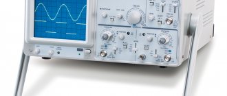
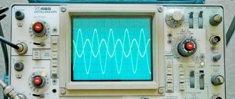
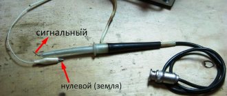
The H313 oscilloscope is needed to observe and study the forms of electrical processes in the frequency range from direct current to 1 MHz thanks to visual observation and measurement of their time and amplitude values.
Working conditions
- Ambient temperature from 10° to 35°.
- Relative air humidity up to 80% at a temperature of 25°.
The oscilloscope should be stored in a dry, heated room at a temperature of 10 to 35° and a relative humidity of no more than 80%.
Instructions on how to use
Preparing for work
Before connecting the device to the network, you must make sure that the fuse installation corresponds to the supply voltage (0.25A for 220 V; 0.5A for 127 V, the 110V fuse socket is not working).
- The device body must be grounded.
- It is necessary to connect the power cable of the device to the electrical network and press the “NETWORK” key. The key backlight should light up.
- A few minutes after startup, you need to adjust the brightness and focus of the scan line using the appropriate knobs.
- After warming up for 20 minutes, the vertical beam deflection amplifier must be balanced.
Schematic of the N-313 oscilloscope
5 911
Without instruments, even the simplest meters, it is difficult, and sometimes even impossible, to “revive” a radio-electronic device created by a radio amateur; repair a TV, radio or tape recorder. However, it is not easy to make a sufficiently high-quality measuring device yourself, and therefore it is especially encouraging that recently more and more such equipment for radio amateurs has appeared on store shelves.
One of them is the N-313 oscilloscope, information about which is given below.
Technical data:
Frequency range of periodic signals, MHz……….0 – 1
Duration of the pulses under study, ms………………………10-3 – 104
Amplitude of the studied signals, V…………………………….10-3 - 300
Amplitude measurement range, V……………………………………5*10-3 - 120
Measuring range of time intervals, ms…………….6*10-3 - 104
Unevenness of the amplitude-frequency characteristic of the vertical beam deflection channel in the range 0-1 MHz, dB, no more than…………………………………±1.6
Minimum beam deflection coefficient, mV/cm…….2.5
Error in measuring the amplitude of alternating and direct voltage levels in the range 0—1 MHz and time intervals in the range 0.8 μs—10 s,%, no more than…………..20
Synchronization of the scan……………………………………… with the signal under study, an external signal (amplitude 0.5 - 30 V), from the network
Input resistance, kOhm. not less…………………………….500
Input capacitance, pf, no more…………………………………….40
Supply voltage, V……………………………………………………127, 220
Power consumption, VA, no more…………………………….18
Dimensions, mm………………………………………………………………………………245x280x70
Weight, kg. no more………………………………………………………3.2
Oscilloscope N313 , which we describe in this issue of the magazine, is manufactured by the Krasnodar electrical measuring instruments plant. Using this oscilloscope, you can not only observe the shape of electrical oscillations, but also measure with sufficient accuracy for amateur practice the main characteristics of electrical signals from direct current to 1 MHz. This is a truly universal measuring device that can be used when setting up both analog and digital devices.
For several months, the H313 oscilloscope was tested in the magazine's laboratory. It has established itself as a reliable and fairly easy-to-use device.
The small-sized portable oscilloscope N313 is designed for observing and studying signal shapes, measuring time and amplitude values of electrical processes in the frequency range from direct current to 1 MHz.
The oscilloscope consists of vertical and horizontal beam deflection channels, a power supply and a 5L038I cathode ray tube.
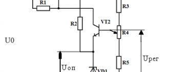
A schematic diagram of the vertical beam deflection channel is shown in Fig. 1.
The signal under study is supplied to “Input 2” and from it, through capacitor C2 (closed input) or directly (open input), goes to a frequency-compensated voltage divider consisting of resistors R13 - R15 and capacitors C6 - C8. The input divider reduces the signal by 100 or 1000 times (by pressing the S1.3 and S1.2 buttons, respectively). When you press buttons S1.4 and 5/.5, the input signal, bypassing the divider, goes directly to the gate of the field-effect transistor V5, connected according to the source follower circuit. Resistor R19 is included in the drain circuit of the field-effect transistor. The voltage released across it controls the operation of transistor V7. As the current flowing through transistor V5 increases, transistor V7 opens, causing the source voltage to drop and the current through transistor V5 to decrease. All this leads to increased stability of the cascade transmission coefficient.
To obtain a zero potential at the output of the source follower, a divider R24R34R35 is included in the drain circuit. Elements R1, R8, R9, VI—V4 protect the source follower from voltage overloads. Capacitor SZ compensates for frequency distortion.
From the source follower, through variable resistor R31, the signal is supplied to the inputs of operational amplifier A1, connected according to a scale amplifier circuit. The operational amplifier through resistor R41 or R44 is covered by negative feedback. When you press the S1.5 button, the feedback coefficient changes by 10 times.
The zero offset voltage at the input of microcircuit A1 is compensated by resistor R43. The R39C12 chain ensures the stability of the operational amplifier A1.
The second large-scale amplifier is made on the A2 chip. The feedback coefficient, determined by the divider R6R7R10R12R17, can be changed using push-button switch S2. When you press buttons S2.1—S2.5, the gain of the scale amplifier is 20, 10, 5, 2 and 1, respectively.
R2 elements. R3 and C1 ensure the stability of the A2 chip. The zero offset voltage of the operational amplifier is compensated by trimming resistor R5.
From the output of operational amplifier A2, the signal goes to the synchronization unit and to the final amplifier, made using transistors V8 and V11 in a balanced circuit. The emitter current of transistors V8, V11 is stabilized by a cascade on transistor V9.
Capacitor C11 compensates for the decline in the amplitude-frequency response of the final amplifier in the high-frequency region. With variable resistor R21 you can move the image on the oscilloscope screen vertically, and with resistor R29 you can adjust (within small limits) the gain of the output stage.
The schematic diagram of the horizontal deflection channel is shown in Fig. 2.
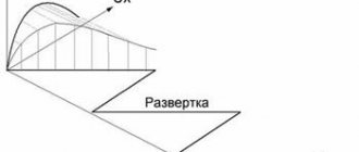
It consists of a synchronization unit and a sweep generator. When you press one of the buttons S1.1—S1.3, the synchronizing signal is sent to the divider R3R4. From part of the variable resistor R4, it is supplied to one of the inputs (selected by switch S1.4) of the operational amplifier A1, on which the clock pulse amplifier is assembled. The second input receives a constant voltage, the level and polarity of which can be changed with a variable resistor R11, thereby adjusting the timing of the scan generator.
The signal from the output of operational amplifier A1 controls the operation of the electronic switch on transistor V6, which, in turn, switches the current in the circuit of the tunnel diode V10.
From the tunnel diode, a short (0.02 μs duration) positive pulse is supplied to the inverter (transistor V15), and then to the trigger (elements D1.1, D1.2). Pulses from the output of element D1.2 control the operation of the scan generator, which operates only in standby mode. The sweep generator includes time-setting capacitors C1—SZ, C5, an electronic switch on transistor V2, cascades for registering the beginning and end of the discharge of time-setting capacitors on transistors V11, V18, respectively, and a charging current stabilizer on transistors V7, V9.
The sweep generator works as follows. In the initial state, the outputs of elements D1.2 and D1.3 are logical “1”, and the outputs of elements D1.1 and D1.4 are logical “0”. From the output of element D1.2, positive voltage is supplied to the base of transistor V2 and keeps it open. The timing capacitors are discharged.
When a short negative pulse from the shaper (transistor V15) arrives at the input of element D1.1 (pin 1), a logical “0” appears at the output of element D1.2, transistor V2 closes and charging of the timing capacitor begins. As soon as the linearly increasing voltage at the output of the source follower reaches a certain level (set by resistor R24}, transistor VII opens and a low logical level is applied to the input of the trigger on elements D1.3, D1.4. From the output of element D1.2, logical “0” is applied to the input of element D1.2 and returns the first trigger to its original state.Transistor V2 opens and the discharge of the timing capacitor begins.
At the end of the discharge, the voltage at the emitter of transistor V18 reaches a level of 0.3-0.4 V. In this case, the trigger on elements D1.3, D1.4 returns to its original state.
The output stage of the scan generator is assembled using transistors V12, V16 according to a circuit similar to the output stage of the vertical deflection channel. Transistor V13 is used to stabilize the current of the output transistors.
The beam reverse suppression unit is assembled on transistor V20.
The schematic diagram of the power supply and the connection diagram of individual components of the oscilloscope are shown in Fig. 3.
12 V voltage stabilizers are assembled on elements V13, V14, R40 and V15-V18, R45 (Fig. 1). The high-voltage rectifier with voltage doubling is made using diodes V19, V21 and capacitors C11. C12, C14. and a high-voltage voltage stabilizer is assembled on zener diodes V3-V6.
Transformer T1 is assembled on one half of the magnetic circuit ШЛ20Х25. Winding 1-2 contains 2000 turns of wire PEV-2 0.13, winding 3-4 - 500 turns of wire PEV-2 0.08, winding 5-6 - 87 turns of wire PEV-2 0.55, winding 7-8, 8-9 - 230 turns of wire PEV-2 0.25, winding 10-12 - 1560 turns of wire PEV-2 0.27, winding 11-12-1140 turns of wire PEV-2 0.23. G.
Krasnodar
RADIO No. 4, 1978, pp. 45-47.
+6
Do you like the diagram? Share with a friend.
Operating procedure
Oscilloscope n313 instructions
You need to press the “INTERNAL SYNCHRONIZATION” key, and set the sweep duration corresponding to the expected period of the signal being studied, and set the “stub” knob to the middle position. Set the “+-” key to the desired position (when synchronizing with a positive signal, the key is released, when synchronizing with a negative signal, roll forward). The size of the picture on the screen is at least three divisions by manipulating the “stub” and “LEVEL” knobs to achieve stability of the picture and the start of scanning at the desired point in the image of the signal under study.
To synchronize the scan with an external signal, press the “EXTERNAL SYNCHRONIZATION” key and apply a signal to the “X” socket. The position of the “+ -” key must correspond to the polarity of the synchronizing signal.
To synchronize from the network, you must press the “NETWORK SYNCHRONIZATION” button.
Checking, setting and adjusting the device
DIY oscilloscope
When using the meter privately, it becomes necessary to do this work with your own hands. To set up and adjust the oscilloscope c1 73, you need to have on hand:
- device diagram;
- high-resistance voltmeter;
- oscilloscope type s1 68 or s1 74;
- digital ampere-voltmeter;
- kilovoltmeters;
- pulse generator G5-41 or similar;
- frequency meter
Schematic diagram of the oscilloscope S1-73
For your information. All the necessary information can be found by studying the description of the device and the operating instructions. There you can find out what elements the device consists of, their parameters, the content of precious metals and the technical characteristics declared by the manufacturer in the accompanying documentation.
The setup is carried out in blocks, based on the device diagram and the required parameters.
The following circuits are checked:
- The built-in power supply is tested with the device turned on:
- Measure the current consumption In = 750 mA. In the warm state, the output voltages are measured and adjusted. At the ends of capacitors 5C7 and 5C8 it should be 18-19 V. Adjustment is carried out with resistance 5R5.
- The frequency of rectangular pulses at pins 4 and 6 of 5Tr1 lies in the range of 8-9 kHz when the duration of opposite-pole half-cycles coincides. Monitoring is carried out with a frequency meter and a test oscilloscope; the converter frequency is adjusted using element 5R21. Similarly, at connections 5С16 and 5С14, the presence of voltage +10 V and -10 V is checked. The permissible discrepancy is 0.2 V for both values. The adjustment is made by rotating 5R18 (–10 V) and 5R14 (+10 V) until the desired values are achieved.
- Using an ampere-voltmeter, check and adjust the potential +80 V with resistor 5R5. Permissible deviations are +75...82 V. Also adjust U = + 2500 V at pin 3 of the high-voltage converter I23.215.069. It should be 2375...2625 V. U = - 650 V is brought to normal (within -630...-670 V), checking with a voltmeter at point 1 of the converter.
- The CRT control circuit is checked and adjusted after operation for 5 minutes. Rotate the “Focus” and “Brightness” knobs to make sure they are working. Achieve installation of the scan line in the middle of the display using the “H” and “C” regulators. By setting the “V/div” switch to the “t5 div” position, shift the meter to the “Calibrator” mode. Check the quality of the picture on the display. If distortion is detected, it is restored by rotating the axis of variable resistance R16. The clarity of the beam is controlled jointly by resistor R18 of the horizontal final stage board and the “Focus” regulator.
- The calibrator is adjusted using a frequency meter connected to the “Y_|_|_ 1 V” socket on the left panel. The output signal at this jack is 1 kHz. The adjustment is performed using a 4R5 resistor. The signal amplitude should not diverge from the nominal value by more than 1V (adjust using 4R4).
- Work with the vertical beam deflection unit is performed when the device is warmed up:
- Switch input switch B2 to “|_”, “V/div” – at the mark “0.05 V”. Place the scan line in the center of the screen. Shift “V/div” to the “0.01 V” position, and use the “Balance” adjustment located on the left wall to return the line to its place. Such manipulations are performed on the “0.05 V”, “0.02 V”, “0.01 V” divisions, ensuring that the strip is in the center at any “V/division” position.
- By setting the “V/div” knob to the “t5 div” mark, turn the “Gain” knob all the way clockwise. The picture must have 5 vertical divisions; the desired result is achieved by adjusting “tV/division” on the left panel.
- The “Gain” knob is moved to the extreme left, “V/div” is set to any of the “0.02 V” or “0.01 V” positions. When the scan line is displaced, the beam is returned to its place with an impedance of 1R12. Look on the preamp board. A static line is achieved at different “Gain” and “V/div” positions.
- By connecting a digital voltmeter to pins 5 and 6 of the preamplifier, reduce the voltage between them to zero using a 1R28 resistor. By rotating 1R18, the potential difference is brought to 0.5 V.
- Again rearrange “V/div” to “t5 div”, “Gain” - all the way to the right. This is achieved using “tB/div” on the left wall of the picture, stretched by 5 divisions vertically. In case of failure, select the value of resistance R14 of the final amplification stage.
- Debugging X-scan. This procedure is performed only after replacing the screen or after repairing the unit.
Knowledge of the design of an oscilloscope, the ability to use the device and repair it help when repairing complex electronic equipment.
