To convert voltage of one level to voltage of another level, pulse voltage converters using inductive energy storage devices are often used. Such converters are characterized by high efficiency, sometimes reaching 95%, and have the ability to produce increased, decreased or inverted output voltage.
In accordance with this, three types of converter circuits are known: buck (Fig. 1), boost (Fig. 2) and inverting (Fig. 3).
Five elements are common to all these types of converters :
- power supply,
- key switching element,
- inductive energy storage (inductor, inductor),
- blocking diode,
- a filter capacitor connected in parallel with the load resistance.
The inclusion of these five elements in various combinations allows you to implement any of the three types of pulse converters.
The converter output voltage level is regulated by changing the width of the pulses that control the operation of the key switching element and, accordingly, the energy stored in the inductive energy storage device.
Stabilization of the output voltage is realized by using feedback: when the output voltage changes, the pulse width automatically changes.
Buck switching converter
The step-down converter (Fig. 1) contains a series-connected chain of switching element S1, inductive energy storage L1, load resistance RH and filter capacitor C1 connected in parallel with it. Blocking diode VD1 is connected between the connection point of the key S1 with the energy storage device L1 and the common wire.
Rice. 1. Operating principle of a step-down voltage converter.
When the switch is open, the diode is closed, energy from the power source is accumulated in an inductive energy storage device. After the switch S1 is closed (open), the energy stored by the inductive storage L1 is transferred through the diode VD1 to the load resistance RH. Capacitor C1 smoothes out voltage ripples.
How does a universal DC-DC converter work?
The principle of its operation has significant similarities with the circuit of a DC boost-type inverter, but in addition a capacitor C1 and a coil L2 are used. Thanks to them, the device is used in voltage reduction mode. Such converters are used in situations where Uin has a large range of values. For example, there are models that convert Uin = 4–35 V to Uout = 1.23–32 V. Externally, a universal converter can be easily recognized by the presence of 2 coils - L1 and L2.
Our previous blog article provides an overview and comparison table of secondary batteries.
Boost switching converter
The step-up pulse voltage converter (Fig. 2) is made on the same basic elements, but has a different combination: a series chain of inductive energy storage L1, diode VD1 and load resistance RH with a filter capacitor C1 connected in parallel is connected to the power source. The switching element S1 is connected between the connection point of the energy storage device L1 with the diode VD1 and the common bus.
Rice. 2. Operating principle of a boost voltage converter.
When the switch is open, current from the power source flows through the inductor, which stores energy. Diode VD1 is closed, the load circuit is disconnected from the power source, key and energy storage device.
The voltage across the load resistance is maintained thanks to the energy stored on the filter capacitor. When the switch is opened, the self-induction EMF is summed with the supply voltage, the stored energy is transferred to the load through the open diode VD1. The output voltage obtained in this way exceeds the supply voltage.
How linear stabilizers appeared
First you need to understand what the main disadvantage of standard linear converters like the LM78XX is. The main element of such a device is a strong bipolar transistor, which was originally a controlled resistor.
The device is included in a Darlington pair. The main current is driven by the operational amplifier. It increases the difference between the output voltage and the one set by the reference voltage source. It is connected using a standard error amplifier circuit.
Connection diagram of the first converters
So, the resistor is switched on using a converter in a series circuit when there is a load. It controls the resistance to extinguish a certain number of volts at the load. When calculating, it can be established that if the voltage decreases, for example, from 12 to 5 V, the input 12 V is distributed to the load and the stabilizer with a ratio of 7:5.
The “excess” 7 V is extinguished and converted into heat. This leads to cooling problems, and a large amount of power is wasted on this. If the power comes from a wall outlet, there is nothing dangerous about it, but if it comes from a battery or battery, this factor must be taken into account.
Using the described method, it would hardly be possible to produce a converter that increases the voltage. About 30 years ago, calculating such schemes was extremely difficult. The simplest circuit of this type is a 2-cycle converter from 5 to 15 V.
Such a device provides galvanic isolation, but the efficiency of its use of a transformer is extremely low. Only 1⁄2 of the primary winding is actively used.
But this is, let's say, a prototype. Now let's talk about modern devices.
Scheme of a modern converter
The microcircuit is convenient to use as a step-down converter. a strong bipolar switch is placed inside, you just need to supplement the regulator with a few more components - a fast diode, output and input capacitors, etc.
The LM2596ADJ variation requires a circuit to provide the output voltage: 2 resistors or 1 plasma resistor.
LM2596 looks something like this from the inside:
The PWM signal is controlled by a powerful key from inside the device. Point A has full voltage for x% of the time, and zero voltage for (1–x)% of the time. Fluctuations are smoothed out by an LC filter. It highlights the constant component of the supply voltage.
Pulse type inverting converter
A pulse-type inverting converter contains the same combination of basic elements, but again in a different connection (Fig. 3): a series chain of switching element S1, diode VD1 and load resistance RH with filter capacitor C1 is connected to the power source.
Inductive energy storage L1 is connected between the connection point of the switching element S1 with the diode VD1 and the common bus.
Rice. 3. Pulse voltage conversion with inversion.
The converter works like this: when the key is closed, energy is stored in an inductive storage device. Diode VD1 is closed and does not pass current from the power source to the load. When the switch is turned off, the self-inductive emf of the energy storage device is applied to a rectifier containing diode VD1, load resistance Rн and filter capacitor C1.
Since the rectifier diode passes only negative voltage pulses into the load, a voltage of a negative sign is formed at the output of the device (inverse, opposite in sign to the supply voltage).
Control method
Frequency converters are controlled in different ways. The main commands include: start, stop, speed control, emergency braking. These actions can be performed both from the inverter panel and from the remote control. This concerns the issuance of commands from the operator to the equipment. The FM can control the operation of the electric drive of motors in the following ways:
Scalar regulation is based on a constant ratio of output voltage and frequency (Uout/Fout). This method does not require the use of a sensor indicating the current position of the rotor. It is used where the loads do not change and there are no increased dynamic loads.
Important! With this adjustment, the load on the engine affects the speed: with a large load the speed decreases, with a small load it increases. The vector method relies not only on control over U/F, but also the angle and magnitude of the space vector (phase)
With this method there is no inertia of adjustment; it is carried out in a wide range of speeds
The vector method relies not only on control over U/F, but also the angle and magnitude of the space vector (phase). With this method there is no inertia of adjustment; it is carried out in a wide range of speeds.
Attention! With the vector method, the load does not affect the rotation speed; constant speed is achieved by automatically adjusting the output voltage
Pulse converters and stabilizers
To stabilize the output voltage of pulse stabilizers of any type, conventional “linear” stabilizers can be used, but they have low efficiency. In this regard, it is much more logical to use pulse voltage stabilizers to stabilize the output voltage of pulse converters, especially since such stabilization is not at all difficult.
Switching voltage stabilizers, in turn, are divided into stabilizers with pulse-width modulation and stabilizers with pulse-frequency modulation. In the first of them, the duration of control pulses changes while their repetition rate remains unchanged. Secondly, on the contrary, the frequency of control pulses changes while their duration remains unchanged. There are also pulse stabilizers with mixed regulation.
Below we will consider amateur radio examples of the evolutionary development of pulse converters and voltage stabilizers.
Units and circuits of pulse converters
The master oscillator (Fig. 4) of pulse converters with an unstabilized output voltage (Fig. 5, 6) on the KR1006VI1 microcircuit operates at a frequency of 65 kHz. The output rectangular pulses of the generator are fed through RC circuits to transistor key elements connected in parallel.
Inductor L1 is made on a ferrite ring with an outer diameter of 10 mm and a magnetic permeability of 2000. Its inductance is 0.6 mH. The efficiency of the converter reaches 82%.
Rice. 4. Master oscillator circuit for pulse voltage converters.
Rice. 5. Diagram of the power part of a step-up pulse voltage converter +5/12 V.
Rice. 6. Circuit of an inverting pulse voltage converter +5/-12 V.
The output ripple amplitude does not exceed 42 mV and depends on the capacitance value of the capacitors at the device output. The maximum load current of the devices (Fig. 5, 6) is 140 mA .
The converter rectifier (Fig. 5, 6) uses a parallel connection of low-current high-frequency diodes connected in series with equalizing resistors R1 - R3.
This entire assembly can be replaced by one modern diode, designed for a current of more than 200 mA at a frequency of up to 100 kHz and a reverse voltage of at least 30 V (for example, KD204, KD226).
As VT1 and VT2, it is possible to use transistors of the KT81x type with a p-p-p structure - KT815, KT817 (Fig. 4.5) and p-p-p - KT814, KT816 (Fig. 6) and others.
To increase the reliability of the converter, it is recommended to connect a diode of type KD204, KD226 in parallel with the emitter-collector junction of the transistor so that it is closed to direct current.
Operating principle
Classic converters with output voltage regulation, as a rule, control the resistance of the element that performs the regulating role (transistor or thyristor), an electric current constantly flows through it, which causes this element to heat up, and a significant part of the power is lost. The main advantage of such a device is a minimum of spare parts, simplicity, and lack of interference. All other characteristics are more related to disadvantages.
The pulse voltage converter uses an adjusting element only in the form of a key. That is, it works in two modes:
- Closed and does not allow electric current to pass through;
- Open and has minimal throughput resistance.
Moreover, each of the modes has low heat generation, which makes it possible to show a high coefficient of efficiency (efficiency). The load continuously receives electricity due to its accumulation and storage in electrical reservoirs such as:
- Inductance (coils);
- Capacitors.
The adjustment occurs by changing the time of the closed state of the key element. Reducing the size and weight of devices is only possible by increasing the frequency, from 20 kHz to 1 MHz. Pulse devices can generate either a reduced voltage or a polarity change at the output. Due to the use of transformers operating at high frequencies, it allows:
- Qualitatively isolate the input from the output;
- Obtain several output voltages at the device output.
Like any device, a pulse converter also has disadvantages, which are:
- The complexity of the circuit and the presence of a larger number of spare parts, which means there are potentially more causes of failure;
- They are sources of interference.
However, the constant development of technology in this direction reduces these disadvantages to a minimum.
Converter with master oscillator-multivibrator
To obtain an output voltage of 30...80 V, P. Belyatsky used a converter with a master oscillator based on an asymmetrical multivibrator with an output stage loaded on an inductive energy storage device - inductor (choke) L1 (Fig. 7).
Rice. 7. Circuit of a voltage converter with a master oscillator based on an asymmetrical multivibrator.
The device is operational in the supply voltage range of 1.0. ..1.5 V and has an efficiency of up to 75%. In the circuit, you can use a standard inductor DM-0.4-125 or another with an inductance of 120...200 μH.
An embodiment of the output stage of the voltage converter is shown in Fig. 8. When a 7777-level (5 V) rectangular control signal cascade is applied to the input of the cascade, the output of the converter, when powered from a 12 V produces a voltage of 250 V at a load current 3...5 mA (load resistance is about 100 kOhm). Inductance of inductor L1 is 1 mH.
As VT1, you can use a domestic transistor, for example, KT604, KT605, KT704B, KT940A(B), KT969A, etc.
Rice. 8. Option for the output stage of the voltage converter.
Rice. 9. Diagram of the output stage of the voltage converter.
A similar circuit of the output stage (Fig. 9) made it possible, when powered from a source with a voltage of 28V and a current consumption of 60 mA to obtain an output voltage of 250 V at a load current of 5 mA . The inductance of the inductor is 600 μH. The frequency of control pulses is 1 kHz.
Depending on the quality of the inductor, the output voltage can be 150...450 V with a power of about 1 W and an efficiency of up to 75%.
Features of LM2596 converters
The most popular application of the device is a voltage source based on a zener diode. It produces a high-quality switching power supply that can withstand the effects of a short circuit. LM2596 - fully complies with the datasheet and all the described parameters.
Another option for using converters is a current stabilizer. The module of this chip connects the LM2596 automotive LED matrix with a power of 10 W, in addition to providing short circuit prevention.
These devices have their own uniqueness. They provide output voltage reduction up to 40 V, requiring only 5 external elements. The voltage of the smart home power bus thus rises to 36 V, and the cross-section of the cables is reduced. In the area of consumption points you need to install such a module and configure it to the required voltage (5,9,12).
Device settings
The microcircuit has the following characteristics:
- Input voltage - from 2.4 to 40 V.
- The output voltage is from 1.2 to 37 V, it can be adjusted and fixed.
- Output current - maximum 3 A.
- Converter frequency - 150 kHz.
- Efficiency at low pressure is 75%, at high pressure it is up to 95%.
Housings
There are 2 types of cases. For one of them, installation inside the hole (TO-220) is used. I like the planar version better, since there the radiator is the board, and there is no need to purchase another external radiator. Mechanically, it is much more stable than the TO-220, which must be screwed to something, for example, to a board. In this case, installing the planar version is much easier.
Dimensions LM2596
I advise you to install the LM2596T-ADJ circuit in the power supply, since it is easier to remove energy from its case.
Voltage converter based on KR1006VI1
A voltage converter based on a pulse generator based on a DA1 KR1006VI1 microcircuit, an amplifier based on a field-effect transistor VT1 and an inductive energy storage device with a rectifier and filter is shown in Fig. 10.
At the output of the converter, with a supply voltage of 9V and a current consumption of 80...90 mA, of 400...425 V is generated . It should be noted that the value of the output voltage is not guaranteed - it significantly depends on the design of the inductor (choke) L1.
Rice. 10. Circuit of a voltage converter with a pulse generator on the KR1006VI1 microcircuit.
To obtain the desired voltage, the easiest way is to experimentally select an inductor to achieve the required voltage or use a voltage multiplier.
Recuperation mode
And what happens if the average value of the magnetic flux of the FSR choke has a sign opposite to ΔФ, for example, if FNACHKON START KON? In this case, according to (7), WIMP
| Figure 9. | Recovery mode. |
When is such a regime necessary? For example, if the converter input is connected to the system power bus, and the output is connected to a battery containing an emergency energy reserve (Figure 10). In normal mode, the system is powered by the main source, and the converter acts as a charger, with energy transferred from the input to the output of the converter, which corresponds to the transfer mode. If the battery is charged, then the energy is not transferred anywhere, and the converter operates in idle mode. In the event of a failure of the main source, energy from the battery through a converter operating in recuperation mode is supplied to the power bus, providing power to the load.
| Figure 10. | An example of the converter operating in three modes. |
It should be noted that the transition from one mode to another occurs automatically, without any participation from the controller, whose main task in this case is only to maintain the required ratio t1/t2 so that, according to (9), provide or the required value of UВХ /UOUT, or required load current.
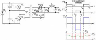
Bipolar pulse converter circuit
To power many electronic devices, a bipolar voltage source is required, providing both positive and negative supply voltages. The diagram shown in Fig. 11 contains much fewer components than similar devices due to the fact that it simultaneously functions as a boost and inverter inductive converter.
Rice. 11. Converter circuit with one inductive element.
The converter circuit (Fig. 11) uses a new combination of main components and includes a four-phase pulse generator, an inductor and two transistor switches.
Control pulses are generated by a D-trigger (DD1.1). During the first phase of the pulses, inductor L1 stores energy through transistor switches VT1 and VT2. During the second phase, switch VT2 opens and energy is transferred to the positive output voltage bus.
During the third phase, both switches are closed, as a result of which the inductor again accumulates energy. When the VT1 key is opened during the final phase of the pulses, this energy is transferred to the negative power bus. , the circuit provides output voltages of ±12 V. The timing diagram (Fig. 11, right) shows the formation of control pulses.
Transistors KT315, KT361 can be used in the circuit.
Voltage converter with stable 30V
The voltage converter (Fig. 12) allows you to obtain a stabilized voltage of 30 V at the output. A voltage of this magnitude is used to power varicaps, as well as vacuum fluorescent indicators.
Rice. 12. Circuit of a voltage converter with a stabilized output voltage of 30 V.
On a DA1 chip of type KR1006VI1, a master oscillator is assembled according to the usual circuit, producing rectangular pulses with a frequency of about 40 kHz.
A transistor switch VT1 is connected to the output of the generator, which switches the inductor L1. The amplitude of the pulses when switching the coil depends on the quality of its manufacture.
In any case, the voltage on it reaches tens of volts. The output voltage is rectified by diode VD1. A U-shaped RC filter and a zener diode VD2 are connected to the output of the rectifier. The voltage at the output of the stabilizer is entirely determined by the type of zener diode used. As a “high-voltage” zener diode, you can use a chain of zener diodes having a lower stabilization voltage.
Voltage converter with inductive energy storage
A voltage converter with an inductive energy storage, which allows maintaining a stable regulated voltage at the output, is shown in Fig. 13.
Rice. 13. Voltage converter circuit with stabilization.
The circuit contains a pulse generator, a two-stage power amplifier, an inductive energy storage device, a rectifier, a filter, and an output voltage stabilization circuit. Resistor R6 sets the required output voltage in the range from 30 to 200 V.
Transistor analogues: VS237V - KT342A, KT3102; VS307V - KT3107I, BF459 - KT940A.
LED Driver
To ensure a stable power supply, you need a special electrical circuit in the form of a power supply unit or driver. It's called led driver.
The electronic circuit ensures stabilization of the voltage and current supplied to the crystal.
This circuit does not automatically support current. It increases with increasing voltage. When its permissible value is exceeded, the crystal will collapse from overheating.
This option is suitable for low-power LED light sources, but it is absolutely not suitable for powerful light emitters. Do not confuse an LED driver with a fluorescent lamp; their operating principles are very different.
Buck and invert voltage converters
Two options - step-down and inverting voltage converters [4.1] are shown in Fig. 14. The first of them provides an output voltage of 8.4 V at a load current of up to 300 mA , the second allows you to obtain a voltage of negative polarity ( -19.4 V ) at the same load current. The output transistor VTZ must be installed on the radiator.
Rice. 14. Circuits of stabilized voltage converters.
Transistor analogues: 2N2222 - KTZ117A 2N4903 - KT814.
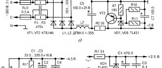
Step-down stabilized voltage converter
A step-down stabilized voltage converter that uses the KR1006VI1 (DA1) microcircuit as a master oscillator and has load flow protection is shown in Fig. 15. The output voltage is 10V when the load current is up to 100mA.
Rice. 15. Step-down voltage converter circuit.
When the load resistance changes by 1%, the output voltage of the converter changes by no more than 0.5%.
Transistor analogues: 2N1613 - KT630G, 2N2905 - KT3107E, KT814.
Output current rise
The chip current is quite high, but sometimes even more is required.
Parallel converters configured for the same output voltage. Under such circumstances, simple smd resistors cannot be used in the circuit that sets the voltage, Feedback. Use resistors with an accuracy of 1% or set the voltage yourself using a variable resistor.
If you are not sure that the voltage spread is small, parallel the converters using a small shunt with a resistance of several tens of mOhms. Then the converter with the highest voltage will take on the entire load, and it is not a fact that it will withstand it.
You can take advantage of high levels of cooling using a large heatsink or a large-area multi-layer PCB. This helps increase the current.
There is another option - placing a powerful key outside the chip body. Therefore, it is possible to use a field-effect resistor with a small voltage drop to increase the efficiency and output current.
Bipolar voltage inverter
To power electronic circuits containing operational amplifiers, bipolar power supplies are often required. This problem can be solved by using a voltage inverter, the circuit of which is shown in Fig. 16.
The device contains a square pulse generator loaded onto inductor L1. The voltage from the inductor is rectified by diode VD2 and supplied to the output of the device (filter capacitors SZ and C4 and load resistance). Zener diode VD1 ensures a constant output voltage - it regulates the duration of the pulse of positive polarity on the inductor.
Rice. 16. Voltage inverter circuit +15/-15 V.
The operating frequency of generation is about 200 kHz under load and up to 500 kHz without load. Maximum load current is up to 50 mA, device efficiency is 80%.
The disadvantage of the design is the relatively high level of electromagnetic interference, which, however, is also typical for other similar circuits.
A DM-0.2-200 throttle was used as L1.
Technical characteristics of the device
The technical characteristics of inverters for the most part coincide with those of classical power supplies. But there are also differences. The pulse converter can operate with a wider input voltage range, has smaller weight and dimensions, and higher efficiency. The devices are characterized by a high level of high-frequency interference, but this can be easily reduced by using filters. Due to the high frequency, the dimensions of the filter are small.
Note! The inverter has a negative input resistance. In practice, this is expressed in the fact that as the supply voltage increases, the current consumption decreases.
You might be interested in Nikola Tesla Electric Generator
Inverters on specialized chips
It is most convenient to assemble highly efficient modern voltage converters using microcircuits specially created for these purposes.
KR1156EU5 microcircuit (MC33063A, MC34063A from Motorola) is designed to operate in stabilized step-up, step-down, and inverting converters with a power of several watts.
In Fig. Figure 17 shows a diagram of a step-up voltage converter based on the KR1156EU5 microcircuit. The converter contains input and output filter capacitors C1, SZ, C4, storage choke L1, rectifier diode VD1, capacitor C2, which sets the operating frequency of the converter, filter choke L2 for smoothing ripples. Resistor R1 serves as a current sensor. The voltage divider R2, R3 determines the output voltage.
Rice. 17. Circuit of a step-up voltage converter on the KR1156EU5 microcircuit.
The operating frequency of the converter is close to 15 kHz at an input voltage of 12 V and rated load. The range of voltage ripples on capacitors SZ and C4 was 70 and 15 mV, respectively.
Inductor L1 with an inductance of 170 μH is wound on three glued rings K12x8x3 M4000NM with PESHO 0.5 wire. The winding consists of 59 turns. Each ring should be broken into two parts before winding.
A common spacer made of PCB with a thickness of 0.5 mm is inserted into one of the gaps and the package is glued together. You can also use ferrite rings with a magnetic permeability of over 1000.
An example of a step-down converter on the KR1156EU5 microcircuit is shown in Fig. 18. A voltage of more than 40 V cannot be supplied to the input of such a converter. The operating frequency of the converter is 30 kHz at UBX = 15 V. The voltage ripple range on capacitors SZ and C4 is 50 mV.
Rice. 18. Scheme of a step-down voltage converter on the KR1156EU5 microcircuit.
Rice. 4.19. Scheme of an inverting voltage converter based on the KR1156EU5 microcircuit.
Choke L1 with an inductance of 220 μH is wound in a similar way (see above) on three rings, but the gluing gap was set to 0.25 mm, the winding contained 55 turns of the same wire.
The following figure (Fig. 4.19) shows a typical circuit of an inverting voltage converter based on the KR1156EU5 microcircuit. The DA1 microcircuit is powered by the sum of the input and output voltages, which should not exceed 40 V.
Converter operating frequency - 30 kHz at UBX=5 S; the range of voltage ripples on capacitors SZ and C4 is 100 and 40 mV.
For inductor L1 of the inverting converter with an inductance of 88 μH, two K12x8x3 M4000NM rings with a gap of 0.25 mm were used. The winding consists of 35 turns of PEV-2 0.7 wire. Inductor L2 in all converters is standard - DM-2.4 with an inductance of 3 μGh. Diode VD1 in all circuits (Fig. 17 - 19) must be a Schottky diode.
To obtain bipolar voltage from unipolar voltage, MAXIM has developed specialized microcircuits. In Fig. Figure 20 shows the possibility of converting a low level voltage (4.5...5 6) into a bipolar output voltage 12 (or 15 6) with a load current of up to 130 (or 100 mA).
Rice. 20. Voltage converter circuit based on the MAX743 chip.
In terms of its internal structure, the microcircuit does not differ from the typical design of similar converters made on discrete elements, however, the integrated design makes it possible to create highly efficient voltage converters with a minimum number of external elements.
Thus, for the MAX743 (Fig. 20), the conversion frequency can reach 200 kHz (which is much higher than the conversion frequency of the vast majority of converters made on discrete elements). With a supply voltage of 5 V, the efficiency is 80...82% with output voltage instability of no more than 3%.
The microcircuit is equipped with protection against emergency situations: when the supply voltage drops 10% below normal, as well as when the case overheats (above 195°C).
To reduce ripple at the output of the converter with a conversion frequency (200 kHz), U-shaped LC filters are installed at the device outputs. Jumper J1 on pins 11 and 13 of the microcircuit is designed to change the value of the output voltages.
To convert low level voltage (2.0...4.5 6) into stabilized 3.3 or 5.0 V, a special microcircuit developed by MAXIM is used - MAX765 . Domestic analogues are KR1446PN1A and KR1446PN1B. A microcircuit for a similar purpose - MAX757 - allows you to obtain a continuously adjustable output voltage within the range of 2.7...5.5 V.
Rice. 21. Circuit of a low-voltage step-up voltage converter to a level of 3.3 or 5.0 V.
The converter circuit shown in Fig. 21, contains a small number of external (hinged) parts.
This device works according to the traditional principle described earlier. The operating frequency of the generator depends on the input voltage and load current and varies over a wide range - from tens of Hz to 100 kHz.
The magnitude of the output voltage is determined by where pin 2 of the DA1 microcircuit is connected: if it is connected to a common bus (see Fig. 21), the output voltage of the KR1446PN1A is 5.0 ± 0.25 V, but if this pin is connected to pin 6, then the output voltage will drop to 3.3±0.15 V. For the KR1446PN1B , the values will be 5.2±0.45 V and 3.44±0.29 V, respectively. The maximum output current of the converter is 100 mA . MAX765 chip provides an output current of 200 mA of 5-6 and 300 mA at a voltage of 3.3 V. Converter efficiency is up to 80%.
The purpose of pin 1 (SHDN) is to temporarily disable the converter by connecting this pin to common. The output voltage in this case will drop to a value slightly less than the input voltage.
The HL1 LED is designed to indicate an emergency reduction in the supply voltage (below 2 V), although the converter itself is capable of operating at lower input voltage values (up to 1.25 6 and below).
The L1 inductor is made on a K10x6x4.5 ring made of M2000NM1 ferrite. It contains 28 turns of 0.5 mm PESHO wire and has an inductance of 22 µH. Before winding, the ferrite ring is broken in half, after being filed with a diamond file. Then the ring is glued with epoxy glue, installing a 0.5 mm thick textolite gasket in one of the resulting gaps.
The inductance of the inductor obtained in this way depends to a greater extent on the thickness of the gap and to a lesser extent on the magnetic permeability of the core and the number of turns of the coil. If you accept the increase in the level of electromagnetic interference, then you can use a DM-2.4 type inductor with an inductance of 20 μGh.
Capacitors C2 and C5 are type K53 (K53-18), C1 and C4 are ceramic (to reduce the level of high-frequency interference), VD1 is a Schottky diode (1 N5818, 1 N5819, SR106, SR160, etc.).
How to make an AC/AC converter
AC/AC and DC/DC converters have identical circuits. Only in AC/AC converters it is necessary to exclude polar elements and use power switches that “... are capable of being either in a closed (conducting) or open (non-conducting) state and allowing current to flow or block the flow in any direction.” If the first condition is intuitive - you cannot use polar elements on alternating current, then the second condition needs to be explained in more detail.
Today, mechanical contacts (for example, relay contacts), semiconductor diodes, bipolar transistors, MOSFETs and IGBTs can be used as power switches from the available element base (Figure 1).
| Picture 1. | Current flow in power elements. |
Diodes, bipolar transistors and IGBTs pass current in only one direction, and the diode is an uncontrolled element. Therefore, these devices cannot be used as independent switches for AC/AC converters. The conductive channel of a MOSFET allows current to flow in both directions, and its resistance is determined by the voltage between the gate and source. In theory, a MOSFET is quite suitable for converting alternating current. However, the presence of a parasitic diode in these devices means that the current cannot be blocked for one of the directions. Thus, the only elements that can be used for the AC/AC converter keys are mechanical contacts. They can either pass current or block its flow in any direction. But mechanical contacts physically cannot switch at high frequencies, have low reliability, high noise levels and many other disadvantages, which is why they are not used in modern converters.
As a result, none of the devices shown in Figure 1 can be used as a full-fledged independent power switch of an AC/AC converter, therefore, in AC voltage converters, the power switches are a combination of several semiconductor devices (Figure 2). Similar circuits are used in matrix converters and are described in detail in.
| Figure 2. | Power switches for AC/AC converters. |
It is immediately clear that these circuits have a serious drawback - current flows through at least two power elements: a diode and a transistor, which negatively affects the efficiency and cost of the converter. But perhaps more effective solutions will appear in the future. For example, RB-IGBT and BD-IGBT are mentioned, but these devices, in terms of their characteristics, availability and cost, have not yet reached a level sufficient for widespread use.
| Figure 3. | Buck (a), boost (b) and inverting (c) AC/AC converters. |
Of the above solutions, the circuit in Figure 2c is of greatest interest, since in it one driver can control two transistors, for which, due to lower control losses, it is better to use MOSFET or IGBT. When using a MOSFET, if the voltage drop across the open channel is less than the forward voltage across the diode, current will flow only through the transistor channels, and the diode will not take part in the conversion process. For IGBT-based switches, you can use devices with a built-in antiparallel diode. This allows you to reduce the number of packages and simplify the board layout, although this reduces the cooling of the crystals
When choosing an IGBT with a built-in diode, you must also pay attention to the thermal resistance of the junction-body of the diode - it should be commensurate with the same resistance of the transistor, because in some devices the diode can have several times greater thermal resistance than the transistor
To build an AC/AC converter, you can take any DC/DC converter circuit, exclude polar elements, and use controlled bidirectional power switches shown in Figure 2 as traditional transistors and diodes. As an example, Figure 3 shows the circuits of classic (basic) AC /AC converters of buck, boost and inverting types. When converting alternating current, they will perform the same functions: lower, raise and invert the input voltage.
Power supply for powering portable and pocket receivers
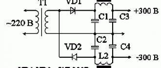
The transformerless power supply (Fig. 23) is designed to power portable and pocket receivers from an AC mains voltage of 220 V. It should be taken into account that this source is not electrically isolated from the supply network. With an output voltage of 9V and a load current of 50 mA, the power supply consumes about 8 mA from the network.
Rice. 23. Scheme of a transformerless power source based on a pulse voltage converter.
The mains voltage, rectified by the diode bridge VD1 - VD4 (Fig. 4.23), charges capacitors C1 and C2. The charging time of capacitor C2 is determined by the circuit constant R1, C2. At the first moment after turning on the device, thyristor VS1 is closed, but at a certain voltage on capacitor C2 it will open and connect circuit L1, NW, to this capacitor.
In this case, capacitor S3 of large capacity will be charged from capacitor C2. The voltage on capacitor C2 will decrease, and on SZ it will increase.
The current through inductor L1, equal to zero at the first moment after opening the thyristor, gradually increases until the voltages on capacitors C2 and SZ are equalized. As soon as this happens, the thyristor VS1 will close, but the energy stored in the inductor L1 will for some time maintain the charge current of the capacitor SZ through the opened diode VD5. Next, the diode VD5 closes, and the relatively slow discharge of the capacitor SZ through the load begins. Zener diode VD6 limits the voltage across the load.
As soon as the thyristor VS1 closes, the voltage on capacitor C2 begins to increase again. At some point, the thyristor opens again, and a new cycle of operation of the device begins. The opening frequency of the thyristor is several times higher than the voltage pulsation frequency on capacitor C1 and depends on the ratings of the circuit elements R1, C2 and the parameters of the thyristor VS1.
Capacitors C1 and C2 are MBM type for a voltage of at least 250 V. Inductor L1 has an inductance of 1...2 mH and a resistance of no more than 0.5 Ohm. It is wound on a cylindrical frame with a diameter of 7 mm.
The winding width is 10 mm, it consists of five layers of PEV-2 0.25 mm wire, wound tightly, turn to turn. An SS2.8x12 tuning core made of M200NN-3 ferrite is inserted into the frame hole. The inductance of the inductor can be varied within wide limits, and sometimes even eliminated completely.
Add a link to a discussion of the article on the forum
RadioKot >Schemes >Power >Converters and UPS >
| Article tags: | Add a tag |
Power inverter for a laptop for a truck 24…28V / 19V 10A.
Author: Provada Yuri Petrovich aka Simurg Published 09.09.2010
2010
The converter brought to your attention will be useful to truck drivers, drivers of trucks with 24 V voltage on board, as well as for those who want to understand the principle of operation and construction of a high-power pulse step-down voltage converter. Trucks usually have two 12V batteries connected in series. Most laptops are designed for 19V. The easiest way to connect a laptop to a linear voltage regulator is as follows:
But that's a long time ago. Now the age of energy saving has come, and spending so much power on heat and then fighting its release is not our method. Our goal is a step-down voltage converter up to 19 V, without generating much heat. For the most powerful laptop at maximum load and charging from scratch, a current of 5:8A is required, and taking into account the reserve, the output current of the converter should be around 10:12A. And this is no longer a small power of 228 W. It is unacceptable to heat the air in the cabin with the power components of the circuit; it is already hot. This article is intended for those who want to understand the operating principle of a switching buck voltage converter. By making this converter, you will gain enough experience to design step-down DC/DC converters yourself. First, I will present a little theory that all of you know. It never hurts to refresh your memory. Basics of energy storage. Equation (1.1), expressing Lenz's rule, contains the definition of inductance. A coil has an inductance of one henry if a change in current of one ampere in one second produces a voltage across the coil of one volt: V=L di/dt. (1.1) The first consequence of equation (1.1) is that the current flowing through an inductor cannot change instantaneously. Indeed, in this case, an infinite voltage would arise on the coil. In reality, such effects as, for example, the electric arc that occurs during the “breakdown” of contacts, limit this voltage to a very high, but not infinite value. The second implication of equation (1.1) is that the voltage across the inductor instantly changes from positive to negative when switching from storing energy in the inductance (the derivative di/dt is positive) to extracting energy from it (di/dt is negative). Let's break down our step-down converter into boxes. In Fig. Figure 1 shows an ideal model of a buck converter, containing an ideal voltage source, an ideal controlled switch, an ideal diode, an ideal inductor, an ideal capacitor and a load resistor.
The converter is a step-down converter because the output voltage is always less than the input voltage, since the voltage at the inductor is opposite to the input voltage (opposite in polarity to the source voltage). This ideal regulator is designed to operate from a 24 V source and provides 19 V into a 2 ohm load. The switch opens and closes every 1 μs, and a pulse-width modulated signal is generated on the passive components. In steady state, the output voltage of the stabilizer is 19 volts = 28 volts * duty cycle. Therefore: duty cycle = 19 volts / 28 volts (0.678 * 100% = 68%) The duty cycle is a value that characterizes the relationship between positive and negative half-cycles in a pulse sequence. This equation determines the output voltage of the converter regardless of the values of inductance, load current and output capacitor, provided that continuous current flows through the inductor. This assumes that the voltage across the inductor has a rectangular shape. In this circuit, a diode is used as a voltage-controlled gate. While the input switch is open, the diode provides a channel for the flow of the inductor discharge current. The voltage across the inductor, when the current flowing through it decreases, has a negative polarity, so the diode opens. When the switch is closed, the inductor stores energy and the diode is reverse biased, so no current flows through it. When designing a buck converter, for simplicity, we will assume that the voltage applied to the inductor during the energy storage process has a perfectly rectangular shape. A good approximation to an ideal rectangular shape is achieved when the voltage fluctuations across the inductor during energy storage are within 0.04 V at an input voltage of 24 V, i.e. 0.16%, and during energy release - 0.04 V at an output voltage of 19 V, i.e. 0.21%. The constant amplitude of the rectangular pulses contributes to the constant di/dt in equation (1.1). In Fig. Figure 1.2 shows the output voltage curve (lower graph) and the inductor current curve (upper graph) in the steady-state mode of the converter, providing a voltage of 19 V and a current of 9.5 A across a 2-ohm load resistor.
Note that the fluctuations in output current are relatively small compared to the DC value in the inductor. In this case, the peak ripple current is 1.4 A. Another important point is that in steady state, the ripple current does not depend on the load current, since the current flowing through the inductor is controlled by the voltage across it. The steepness of the current rise and the duration of the energy accumulation phase are determined solely by the voltage difference Vin-Vout. The average inductor current is equal to the output current. c The buck converter can also operate in a discontinuous mode, in which the inductor current is zero for some part of the switching period. For intermittent operation, equation (1.1) is not valid. The output voltage ripple in a step-down converter is higher because the filter capacitor must supply the load current when the inductor current is zero. Typically, a buck converter operates in intermittent mode only when the load current becomes much less than its rated design value. Operating modes of the inductor (continuous and intermittent current) - when the inductance increases above a certain value (depending on the load), the inductor current stops decreasing to zero during each period. Inductance in this case affects the current increment during the open state of the switch. If W(I) =(L*I^2)/2 is the dependence of the energy accumulated in the inductor on the current, then in continuous mode the energy transmitted in one period will be W = W(I0 + deltaI) - W(I0), where I0 - current in the inductor at the moment the key transistor is turned on. The duty cycle in continuous current mode does not depend on the load. As the load increases, the inductor current increment (deltaI) remains constant, but I0 increases - due to which any output power will be provided at any inductance value. In continuous current mode, with a further increase in inductance, the shape of the switch current approaches rectangular pulses (accordingly, the peak current decreases). The inductor current increment is practically independent of the switch resistance. It is defined as Uin*ton/L. Of course, in reality, the power will be limited by one of the following factors: 1) losses on active resistance (switch, inductor, diode), 2) saturation of the inductor magnetic circuit (as a consequence, point 1), 3) transition of the key transistor to active mode (again , as a consequence, point 1), 4) limited range of duty cycle regulation by the PWM controller And much more. During normal operation of the key, the voltage drop across it in the open state is much less than the supply voltage. Accordingly, the current in the inductor increases almost linearly, in accordance with the law di=U*dt/L. If it comes to the point that the active resistance of the key significantly affects the operation of the converter, you need to install a different key. Too little inductance will require too much peak switch current, but will store energy. An arbitrarily large amount of inductance will not limit the output power, even if the operating frequency is not changed. The converter will operate in continuous inductor current mode with all the consequences. In general, the optimal inductance depends on the frequency, input voltage, and output power (and the optimality criteria may be different). If you use a larger inductance (at the same conversion frequency and output power), nothing bad will happen. A larger inductor will be required, but the peak current of the switch will be reduced. The inverter will start to operate in continuous current mode after the load exceeds a certain threshold. The shape of the key current in this mode is trapezoidal. At the moment the device is turned on, the inductor current is zero; with one turn on of the key, it will increase to Upit*ton/L. In the next period, by the time the key is turned on, the inductor current does not have time to drop to zero, which is the actual difference between the continuous current mode and the intermittent one. With each subsequent period, the initial inductor current (at the moment the switch is turned on) increases. This happens until the converter reaches a steady state (for a certain number of periods). In steady state (continuous current), with a sufficiently large inductance (any finite value), the peak current of the inductor is almost equal to the average (current ripple is much less than the average value), average current = Iout*Uout/Uin (without taking into account losses). The choke works like a kind of transformer. In continuous current mode, the duty cycle does not depend on the load. The switch on time is ton = (1/f)*(Vout-Vin)/Vout (without taking into account losses). The transfer functions of the converter in intermittent and continuous current modes are different. If in the first case the inductor works as an energy storage device, then in the second - as a transformer (approximately).
Synchronous rectification
All of the circuits discussed in this chapter use diodes as voltage-controlled switches. Shifted in the opposite direction, they represent open keys, and in the forward direction, they are closed. MOSFETs can also act as switches. If the gate-source voltage is sufficient to turn on the transistor, current can flow through the transistor in one direction or the other. Field-effect transistors used as switches have an open resistance of 0.01 Ohm and below. The voltage drop across a Schottky diode at a current of 10 A is approximately 0.6 V, and the dissipation power is 6 W. A field-effect transistor with a resistance of 0.01 Ohm at a current of 10 A dissipates power of 0.1 W. Therefore, the use of a field-effect transistor significantly increases the efficiency of the converter. In Fig. Figure 2 shows a buck regulator using a synchronous rectifier and ideal passive components. This circuit uses an IC chip, an ideal buck converter controller, to control the FETs and provide voltage feedback. When Q1 closes, Q2 opens for a short time to reset the maximum current at the initial moment, then the Schottky diode operates at a low residual current. This example shows only a buck converter, but it is possible to replace diodes with MOSFETs in all types of converters in a similar manner.
In our downconverter, the pulse repetition rate is constant, but their width varies, i.e., pulse-width modulation (PWM) is used, and it is easier for us to ensure electromagnetic compatibility than in a circuit with pulse-frequency modulation, and the ripples at the output of the circuit are more predictable and controlled. The basic circuit of a voltage-controlled PWM controller is shown in Fig. 3.
The output voltage of the converter is fed through a voltage divider to the non-inverting input of the error amplifier, at the output of which an error (mismatch) signal scaled, taking into account the reference voltage, is formed. To generate a sawtooth signal of a constant frequency, a multivibrator is used, such as in the KR1006VI1 microcircuit. As a rule, the charging current of the timing capacitor is determined by the resistance of the timing resistor. When the voltage across the capacitor reaches the trigger point, the trigger included in the ramp voltage generator (RVG) is turned on and the capacitor is quickly discharged to the release voltage. As a result of comparing the voltage at the output of the error amplifier and the GPG voltage, a control signal for the output switch of the converter is generated, which is illustrated by the graph:
When the GPG voltage is less than the output voltage of the error amplifier, the switch opens (closes). When the GPG voltage exceeds the output voltage of the error amplifier, the switch opens. If the error voltage is less than the minimum value of the ramp voltage, then the duty cycle is 80%; If the error voltage exceeds the maximum ramp voltage value, the duty cycle is 0%. In flyback and boost converters, it is necessary to ensure a certain minimum value of the interval between pulses, that is, the duty cycle should not reach 100%, so that the energy accumulated in the inductor can be transferred to the output circuit. Some forward converter circuits also require a certain value for the interval between pulses. Modern voltage-controlled PWM controllers are equipped with a mechanism that ensures a duty cycle of less than 100%.
PWM current control has its advantages over voltage control. These include improved transient response and a simpler control loop. In Fig. Figure 4 shows a typical circuit of a PWM controller with current control (type UC3842 - UC3845). This circuit uses a constant frequency pulse generator.
The next pulse from the generator arriving at the setting input (S) of the RS trigger sets its output to a HIGH level, which leads to the opening of the transistor switch. When the voltage across the current-measuring resistor is Lizm. reaches the value of the comparator response voltage set by the error amplifier, the latter “resets” (switches) the trigger, as a result of which the switch opens (current no longer flows through the transistor). An error amplifier is used to adjust the current switch actuation point so that the inductor current is sufficient to maintain the output voltage. As the output voltage reaches the desired value, the error signal "steps down" the operating current to keep the average inductor current constant.
Further, specifically according to our circuits: The first circuit (finished board), not of high power, is suitable for a small laptop or netbook with a maximum current of 4 amperes.
Conversion frequency 78 kHz. During testing, it turned out that when approaching maximum power, the output switch lacks a driver. (To correct this drawback, you can build it on the LM3477, which already has a built-in driver. Datasheet for it https://www.nscrus.ru/content/catalog/pdf/LM3477.pdf
or in general, if laziness overpowers, without a transistor on LM2677 (see datasheet at https://www.nscrus.ru/content/catalog/pdf/LM2677.pdf)). Since cats don’t look for easy ways, we experiment and explore our schemes. The LM3578 circuit works and has been tested many times. There is no current limitation in this circuit, and it is afraid of a short circuit in the load. Be careful. The choke is wound on a yellow ring with one white side. The inductance of the inductor is 88 μH, but up to 100 μH is possible. Approximately 50-65 turns of PEV-2 0.6 mm evenly distributed around the ring. The circuit is assembled on the LM3578 MS. Datasheet for it here: https://www.datasheetcatalog.org/datasheet/nationalsemiconductor/DS008711.PDF Output transistor here: https://www.datasheetcatalog.org/datasheet/cet/CEM9435A.pdf
Type of printed circuit board:
To protect against overvoltage during transistor breakdown, a 20 volt 1.5KE20A suppressor is used paired with a 5 ampere fuse. The chip is not expensive, but more expensive than MC34063. In this circuit there is no synchronous rectification and the diode heats up to 85 degrees, which is not good. In the next circuit we will use synchronous rectification on an n-channel field-effect transistor to increase efficiency by 5 - 10%.
Powerful Buck Converter with Synchronous Rectification
Scheme:
This is a buck converter with synchronous rectification. This type of converter is the best option, since at high power synchronous rectification gives us an increase in efficiency by 5-10%, while not greatly complicating the circuit. The control microcircuit MC34063 is the most affordable. The microcircuit is produced by a large number of manufacturers. MC34063 is not very suitable for small loads when working on an additional key, and not on its built-in one. If the power is installed in excess, it switches on the skipping mode at low load, which will result in increased noise in the output voltage. But this is found in many power controllers. For example, in the same TNY26x. Only in MC34063 this is done simply. If you want to make sure of the similarity, then take, for example, the well-known UC3842, about which it is clearly written that it is a “PWM controller with current feedback.” What happens if the Vfb input falls below 1.3V? Yes, the same as the MC34063 - the UC3842 will transmit pulses. This, by the way, is one of the ways to block it (pulling the signal on Vfb to the PGND potential). To power a powerful laptop, using the MC34063 as a control chip is quite acceptable. The main advantages of MC34063 are low cost, minimum additional wiring, shunt in the positive circuit. But of course you can install both UC3843 and UC3842 here (if UC3842, then the supply voltage must be raised to 16.3V) with the appropriate wiring, but then the shunt will be on the negative wire, which is very bad. Then you cannot connect to the diagnostic connector of the car itself while simultaneously receiving power from the converter. The shunt will be short-circuited in this case. Next according to the diagram is the driver. Driver for power transistors IR2183 (price about 3 USD). One of its inputs is direct, the second is inverse, and an external inverter is not needed for synchronous rectification. The chip has built-in logic that prevents the simultaneous unlocking of both transistors (through currents) and a pause generator (“dead time”) between output pulses. The microcircuit has powerful outputs for controlling output field-effect transistors - 1.7A. The differentiating circuit R6, C4 - for the operation of the lower transistor in the synchronous rectifier, allows the driver to turn it on only at a short moment in time, immediately after the upper transistor closes. At this short moment, the current flowing through the transistor is maximum. Subsequently, when the current is already minimal, a 45-volt Schottky diode operates from a computer power supply with a 5-volt channel. If you do not install the circuit R6, C4, but connect pins 2 and 3 together, the lower level transistor will be open more than necessary, thereby short-circuiting the output capacitor. A field-effect transistor VT2 was used as a diode - for diodes the voltage drop across the junction is 0.8V, for Schottky diodes it is 0.6V, here it is about 0.1V. For optimal operation of the transistor, the R6C4 chain and the R7R8 divider are selected. To protect against load short circuits and limit the output current, a protection unit built into the MC34063 chip operates. Resistor R12 is a current sensor; if the voltage drop across this resistor is more than 300 mV, MC34063 will reduce the duration of the pulses at its output, and the voltage at the output of the converter will decrease accordingly. To power the driver microcircuit and the collector of the output transistor in the MC34063, the supply voltage is 15 V. Filtering electrolytic capacitors are made up of several parallel-connected capacitors of smaller capacity and shunted with ceramic SMDs. These capacitors are a little warm when operating. At a load current of 5:6 A, the heating of the entire converter is less than 40 degrees at an ambient temperature of 28 degrees. The choke was taken as an experiment from a computer power supply of a 3.3 volt channel and was not rewound. During tests it showed good performance and does not get very hot. Its inductance is 51 μH. The choke is wound on a yellow ring with one white side. I left it like that, although it could have been rewound with a few wires to reduce the skin effect. Assembly process: The board is made using LUT technology.
We clean it and cover it with an alcohol-rosin solution (the author keeps it in an oil dish, so it’s easier to use), then dry it with a hot air gun so that it doesn’t stick to your hands during the assembly process. Photos step by step. Clean off the toner with sandpaper:
The board was designed for such a heatsink
Finished board:
The upper side of the negative conductor is connected to the lower side along the very edge of the board with the input-output track and is a screen.
Setup. We connect to the power supply via a 24 V, 1:2 A light bulb. The voltage at the output of the converter is about 19 V, the power light does not light. During operation, the converter should not be excited, and no cracking noise should be heard. Now, instead of a light bulb in the power circuit, we install an ammeter with a measurement limit of more than 20 A, and connect a nichrome spiral with a current of 8 A to the output (i.e., its power is 24:48 W). The current consumed by the circuit from the battery should be approximately 1.3 times less than the coil current, both field-effect transistors should not get too hot and the temperature of both transistors should be the same. If the lower transistor does not heat up at all, but the diode noticeably heats up, then you need to make sure that there is a signal at its gate. Setting up a synchronous rectifier: Instead of R6, connect a tuning resistor and slowly rotating it, look at the current consumed by the circuit. It will begin to decrease - by about 5:10%. This current was previously consumed by the Schottky diode. If you rotate it further, the current consumed by the circuit increases sharply several times. We install the engine in a position where the current consumption has decreased, but is far from a sharp increase. All electrolytes must be collected from several parallel-connected capacitors, but of smaller capacity, and multilayer SMD ceramic capacitors with a capacity of 1 μF or more must be connected in parallel with them. The power traces should be thicker and carefully tinned with a thick, thick layer of chocolate solder. If excitation occurs, most likely there are not enough ceramic shunt capacitors for power supply. The above inverters can easily be converted to an output voltage of 12 volts by only changing the voltage feedback resistor to a different value. Now some oscillograms: The output is 34063. The driver and transistors are not yet connected. 34063 at maximum width.
From the output of the lower key driver
And it's more extended
Regarding transistors: The author used output transistors, carefully broken out from UPSs whose batteries had failed. Photos of transistors for the converter:
For the case, we’ll take a ready-made purchased box-case priced at $1.5
Photo of the assembled converter being tested. Output current 7 amperes 19 volts. Under the radiator, a large hole was cut out with nichrome wire for the board, which falls into it up to the radiator. The inscription opposite the LEDs “Safety is damaged” means that the fuse has burned out, and “Accum. Discharged" - the battery is dead. Battery discharge indicator diagram:
As a result of the research, a step-down converter from 28 to 19 volts was obtained for any laptop with a high efficiency of 84 - 90% depending on the input voltage, and a rated current of 10A. Successful experiments, as well as exciting and educational work. Thank you for your patience in reading the article.
Files:
Printed circuit boards in SL 5.0 format.
As usual, we put the questions here.
| What do you think of this article? | Did this device work for you? | |
| 24 | 1 | 0 |
Schemes of devices for energy conversion
Diagrams of devices for energy conversion are shown in Fig. 4.24 and 4.25. They are step-down energy converters powered by rectifiers with a quenching capacitor. The voltage at the output of the devices is stabilized.
Rice. 24. Scheme of a step-down voltage converter with transformerless mains power supply.
Rice. 25. Option of a step-down voltage converter circuit with transformerless mains power supply.
As VD4 dinistors, you can use domestic low-voltage analogues - KN102A, B. Like the previous device (Fig. 23), power supplies (Fig. 24 and 25) have a galvanic connection with the supply network.
How is the output current regulated?
This is only possible if we are dealing with an adjustable output voltage in the LM2596ADJ variant. In China, just such a board is produced, which has all kinds of indications. This module can be purchased under the name xw026fr4.
xw026fr4
If you do not want to use a ready-made module, make the device yourself. It is not difficult. There is only one problem - the microcircuit does not control the current, but this can be changed.
A current converter is a current device used in light and laser diodes, galvanic cells, and chargers. You can purchase it in popular online stores.
Voltage converter with pulse energy storage
In the S. F. Sikolenko voltage converter with “pulse energy storage” (Fig. 26), switches K1 and K2 are made on KT630 transistors, the control system (CS) is on a K564 series microcircuit.
Rice. 26. Circuit of a voltage converter with pulse accumulation.
Storage capacitor C1 - 47 µF. A 9 V battery is used as a power source. The output voltage at a load resistance of 1 kOhm reaches 50 V. The efficiency is 80% and increases to 95% when using CMOS structures such as RFLIN20L as key elements K1 and K2.
Properties of inverters [edit | edit code ]
- Voltage inverters make it possible to eliminate or at least weaken the dependence of the operation of information systems on the quality of alternating current networks. For example, in personal computers, in the event of a sudden network failure, with the help of a backup battery and an inverter, forming an uninterruptible power supply
(UPS), it is possible to ensure that the computers operate to correctly complete the tasks being solved. In more complex critical systems, inverter devices can operate in a long-term controlled mode in parallel with the network or independently of it. - In addition to “independent” applications, where the inverter acts as a power source for AC consumers, energy conversion technologies have become widely developed, where the inverter is an intermediate link in the chain of converters. The fundamental feature of voltage inverters for such applications is the high conversion frequency (tens to hundreds of kilohertz). Effective energy conversion at high frequencies requires a more advanced element base (semiconductor switches, magnetic materials, specialized controllers).
- Like any other power device, the inverter must have high efficiency, high reliability and acceptable weight and size characteristics. In addition, it must have an acceptable level of higher harmonic components in the output voltage curve (acceptable value of harmonic coefficients) and not create during operation a level of ripple at the terminals of the energy source that is unacceptable for other consumers.
- In pure metering systemsGr > Inverter operation
The operation of a voltage inverter is based on switching a constant voltage source to periodically change the polarity of the voltage at the load terminals. The switching frequency is set by control signals generated by the control circuit (controller). The controller can also solve additional tasks:
- voltage regulation;
- synchronization of key switching frequency;
- protecting them from overloads, etc.
According to the principle of operation, inverters are divided into:
- voltage inverters (VIN), example - inverters of most UPSs;
- current inverters (AIT), example - Soviet airfield converter APChS-63U1;
- resonant inverters (AIR);
dependent (inverters driven by the network), an example is the power converter of electric locomotives VL85, EP1, etc.
Pulse-resonant converter
Pulse-resonant converters designed by the so-called. N. M. Muzychenko, one of which is shown in Fig. 4.27, depending on the shape of the current in the VT1 switch, they are divided into three types, in which the switching elements close at zero current and open at zero voltage. At the switching stage, the converters operate as resonant converters, and the rest, most of the period, as pulse converters.
Rice. 27. Scheme of a pulse-resonance converter N. M. Muzychenko.
A distinctive feature of such converters is that their power part is made in the form of an inductive-capacitive bridge with a switch in one diagonal and with a switch and power supply in the other. Such schemes (Fig. 27) are highly efficient.
Source: Shustov M. A. Practical circuitry. Voltage converters.
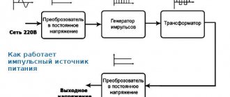
Operating principle of a switching power supply
The operation of the inverter is based on the rectification of the primary voltage and its further conversion into a sequence of high-frequency pulses. This differs from a conventional transformer. The output voltage of the block serves to generate a negative feedback signal, which allows you to adjust the pulse parameters. By controlling the pulse width, it is easy to organize stabilization and adjustment of output parameters, voltage or current. That is, it can be either a voltage stabilizer or a current stabilizer.
The number and polarity of output values can be very different depending on how the switching power supply operates.