Bipolar voltage stabilizers for microcontrollers
If there are positive voltage stabilizers, then logically there should also be negative voltage stabilizers. They are built according to complementary symmetrical schemes, i.e. with a different conductivity structure of transistors and with opposite polarity of inclusion of diodes, zener diodes, electrolytic capacitors.
The classification of negative and positive voltage stabilizers is the same: parametric on zener diodes and compensation on integrated circuits. In the latter case, the similarity of names helps. For example, the equivalent for the "positive" series 78xx is the "negative" series 79xx.
The negative voltage stabilizer itself is of no interest (everything in the world is relative!). The effect of its use is observed only with bipolar nutrition. This need arises, in particular, if the device, in addition to the MK, uses external op-amps, switches, and ADCs.
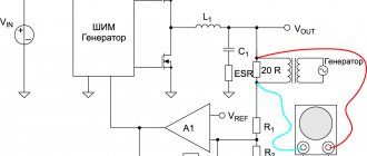
Smoothing electrolytic capacitors are installed at the outputs of positive and negative voltage stabilizers. In small-sized equipment, it is convenient to use “SMD columns” with a capacity of 1...10000 μF, designed for an operating voltage of 6.3... 100 V. In addition, when choosing the type of electrolytic capacitor, dynamic parameters must be taken into account. The most indicative of them are the limiting ripple current RIPPLE (Ripple Current) - the higher it is, the better, as well as the equivalent series resistance ESR (Equivalent Series Resistance, in Russian EPS) - the lower it is, the better. Dynamic parameters for foreign capacitors are standardized at a frequency of 120 Hz or in the range of 100...300 kHz.
A capacitor rated for higher voltage has lower ESR resistance. For example, a capacitor of 1000 μFxb.3 V according to the datasheet has ESR = 53 mOhm, and a capacitor of 1000 μFx16 V according to the datasheet has ESR = 23 mOhm. A further increase in voltage from 16 V to 35 ... 100 V does not lead to a noticeable decrease in ESR. Therefore, when powering the MK from 5 V, it is better to place capacitors with a voltage of 16 V between Uss and GND, and not 6.3 V (at the same time, the reliability of operation increases).
The ESR of one “large” capacitor is usually higher than the ESR of two parallel capacitors of half the capacitance, as can be seen from Table. 6.4, therefore it is beneficial in terms of power supply to solder many “small” capacitors, evenly distributing them on the printed circuit board.
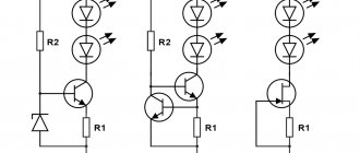
In Fig. 6.7, a...e shows parametric diagrams, and Fig. 6.8, a...d - compensating bipolar voltage stabilizers.
Rice. 6.7. Circuits of parametric bipolar voltage stabilizers {beginning)'.
a) two half-wave rectifiers on elements VDI, C1 and VD2, C2 provide bipolar power. Identical zener diodes VD3, VD4 create approximately equal load on transformer 77 at positive and negative half-waves of the mains voltage. This is necessary to eliminate magnetization of the core of transformer 77. For the same purpose, a two-color (rather than single-color) power indicator HL1 is used, which conducts current alternately in both directions and glows a total yellow color;
b) full-wave bridge rectifier with a midpoint in the secondary winding of transformer 77. Two voltage stabilizers are made according to symmetrical circuits. They contain zener diodes VD2, VD3 and current amplifiers on transistors VTI, VT2. The ripple frequency of the full-wave circuit is 100 Hz, which is useful when calculating the required capacitance of capacitors C1...C4
c) a source of asymmetrical bipolar power supply using GBI, GB2 batteries. The stabilization effect is created by the batteries themselves, since they maintain an almost unchanged voltage at their terminals for a long time; ABOUT
Rice. 6.7. Schemes of parametric bipolar voltage stabilizers (end):
d) receiving bipolar stabilized voltage from a three-phase 380 V network. Capacitors C1...SZ are ballast. Reduction of ripple at the input is carried out by filters L1, C4, L2, C5, and at the output - by capacitors C6, C7. Transistors VTI, VT2 are used with the same conductivity, since there are no three-terminal zener diodes VD7, VD8 reverse, i.e. "negative" polarity. A similar circuit design can be used in a 220 V network, supplying alternating voltage from the diode bridge directly to the inductors L1, L2. The capacitance of all electrolytic capacitors of the filter will have to be increased, since in a three-phase rectifier the pulsation frequency is higher;
e) bipolar power supply from battery GB1 with an artificial midpoint on a low-resistance divider RI, R2. The stabilizer itself is the battery itself, which maintains a slightly varying voltage at its terminals until the moment of complete discharge. Capacitors C1...C5 reduce the impedance of the power supply at low and high frequencies. For the purpose of unification, all electrolytic capacitors can be chosen to be the same at 16 V, despite the fact that the operating voltage of capacitors C2, SZ may be less than that of C1;
e) bipolar power supply is provided by two three-terminal zener diodes VDI, VD2. If bipolar power is not required, then you can use unipolar 5 V by connecting the GND common wire to the -2.5 V circuit, and the positive Vcc pin to the +2.5 V circuit.
Rice. 6.8. Schemes of compensating bipolar voltage stabilizers:
a) organization of an artificial midpoint from a single power source. The compensation stabilizer DA 1 is located in the positive voltage channel, and the parametric stabilizer on diodes VD2 ... VD4 is in the negative voltage channel;
b) the DAJ chip lowers the input voltage to +5 V, and the DA2 converter (Calogic Corporation) inverts the polarity while maintaining the absolute value. The total load current in the +5 and -5 V circuits should not exceed 100 mA (the maximum permissible current for DA1). The voltage in the -5 V channel depends on the load outflow more than in the +5 V channel;
c) bipolar voltage stabilizer based on complementary microcircuits DAI, DA2. Diodes VD2, VD3 protect radioelements in the +5 and -5 V channels from reverse voltage supply. This can happen during an accident or transient processes, when one of the voltages is temporarily absent. If the resistance Rn is very high, then diodes VD2, VD3 are not needed;
d) stabilizers DAI, DA2 of the same type, but in an “inverted” connection.
Source: Ryumik S.M. 1000 and one microcontroller circuit.
Transistor voltage stabilizer
- Stabilizer on one zener diode
- Stabilizer on one transistor
- Transistor stabilizer with short circuit protection
- Stabilizer with adjustable output voltage
Stabilizer on one zener diode
To smooth out voltage ripples and constant current at the output of the power supply, stabilizers are used.
As a rule, the stabilizer is based on a zener diode. Zener diode is a semiconductor device with voltage stabilization properties. Unlike a conventional diode, it operates in reverse polarity (plus is supplied to the cathode), in avalanche breakdown mode. Due to this property of the zener diode, the voltage on it, and therefore on the load, practically does not change. The figure below shows a diagram of a simple stabilizer. This stabilizer is suitable for powering low-power devices.
The principle of operation of the stabilizer on a zener diode
A capacitor is needed to smooth out voltage ripples; it is called a filter. A resistor is needed to smooth out current ripples and is called a damping resistor. The zener diode stabilizes the voltage across the load. For normal operation of this circuit, the supply voltage must be greater than 40...50%. The zener diode should be selected for the voltage and current we need.
Stabilizer on one transistor
To power a higher power load, a transistor is added to the circuit. An example circuit is shown below.
The principle of operation of a stabilizer on a single transistor
The chain of R1 and VT1 is already familiar to us from the previous circuit; this is the simplest stabilizer; it sets a stabilized voltage based on transistor VT2. The transistor, in turn, performs the function of a current amplifier and is a control element in this circuit. For example, as the input voltage increases, the output voltage will tend to increase. This leads to a decrease in the voltage at the emitter junction of transistor VT2, which leads to its closure. In this case, the voltage drop in the emitter-collector section increases so much that the voltage on the zener diode decreases to the original level. When the voltage drops, the stabilizer reacts in the reverse order.
Transistor stabilizer with short circuit protection
In the practice of a radio amateur, mistakes occur and a short circuit occurs. To reduce the consequences of a short circuit, consider a stabilizer circuit for two fixed voltages and with short circuit protection.
As you can see, transistor V4, diodes V6 and V7 have been added to this circuit, and a parametric stabilizer consisting of resistor R1, diodes V2, V3 is equipped with switch S2.
Operating principle of stabilizer protection
This circuit is designed for a short-circuit response current of 250...300 mA; as long as it is not exceeded, the current will pass through a voltage divider consisting of diode V7 and resistor R3. By selecting this resistor, you can adjust the protection threshold. Diode V6 will be closed and will not have any effect on the work. When the protection is triggered, diode V7 will close, and diode V6 will open and bypass the zener diode connections, while transistors V4 and V5 will close. The load current will drop to 20...30 mA. Transistor V5 should be installed on the heat sink.
Stabilizer with adjustable output voltage
When repairing or adjusting electronic devices, it is necessary to have a power supply with an adjustable output voltage. A schematic diagram of voltage-regulated stabilizers is presented below.
The principle of operation of a stabilizer with voltage regulation
A parametric stabilizer consisting of R2 and V2 stabilizes the voltage across the variable resistor R3. The voltage from this resistor is supplied to the control transistor. This transistor is connected according to the emitter follower circuit, the load of which is resistor R4. The voltage from resistor R4 is supplied to the control transistor V4, the load of which is already our powered device. Voltage regulation is carried out by variable resistor R3; if the resistor slider is in the minimum position according to the circuit, then the voltage to open transistors V3 and V4 is not enough and the output will have a minimum voltage. When the engine rotates, the transistors begin to open, which increases the voltage across the load. As the load current increases, the voltage drop across resistor R1 and lamp H1 begins to light up; at a current of 250 mA, a dim glow is observed, and at a current of 500 mA and above, a bright glow is observed. Transistor V4 should be installed on the heat sink. With an increased load of more than 500 mA, you should turn off the power supply as quickly as possible, since under prolonged maximum load the diodes in the rectifier bridge and transistor V4 fail.
These circuits, when assembled correctly, do not require adjustment. They can also be upgraded to higher currents and voltages. By selecting radioelements with the parameters we need.
That's all. If you have comments or suggestions regarding this article, please write to the site administrator.
Good luck!