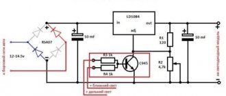
Turning on the ignition when starting the car or releasing a large amount of energy into the electronics when the engine is turned off are sources of dangerous voltage surges in the 12 V car network. Such conditions are divided into low voltage (UV) and high voltage (OV); they can have significant voltage levels and damage circuits not designed to withstand such extreme conditions. Special devices have been developed to protect sensitive electronics from power transients.
The LTC4368 microcircuit is an example of such a specialized device for protecting against under- and overvoltage in a car electrical network. It uses a comparator for control. The supply voltage is controlled by a resistive voltage divider connected to the UV and OV monitoring pins. The output of the comparator controls the gates of two N-channel MOSFETs, which in turn control the current connection between the battery and the load.
The LTC4368 comparator is designed with only 25 mV hysteresis at the monitor pins for improved noise immunity. Hysteresis can prevent MOSFETs from turning on or off falsely due to, for example, ripple or high-frequency oscillations in the power line. The 25 mV hysteresis in the LTC4368 corresponds to 5% of the monitor pin thresholds and is common to both under- and over-voltage protection.
For safety or to reduce the load on the ignition line, some automotive auxiliary circuits must be disconnected from the electrical system when starting or stopping the vehicle. Due to the large amplitude transients, these circuits may require even greater hysteresis than the LTC4368 itself. In such applications, higher hysteresis requirements can be met by setting the LTC4368 to monitor the power supply of a hysteresis-adjustable chip such as the LTC2966. The figure shows an example of protecting an automotive circuit with a wide voltage range. In this circuit, the LTC2966 acts as a comparator and the LTC4368 is responsible for connecting the load to the network.
Protective power control device in a car
Power line control with wide voltage monitoring hysteresis - diagram
The solution shown in the figure above protects electronics that are sensitive to transient conditions - dips, surges and overcurrents that occur in the car's power source.
The LTC2966 monitors both reverse voltage and forward voltage that is too low or too high. Control thresholds and hysteresis levels are adjusted by resistor circuits on the INH and INL pins and voltages on the RS1 and RS2 pins. OUTA is the output of the UV comparator and OUTB is the output of the OV comparator. The polarity of these outputs can be selected to be reverse or normal to the inputs using the PSA and PSB pins. In the figure they are configured as non-inverting. The OUTA and OUTB pins from the LTC2966 are connected to the REF pin of the LTC2966 and are fed directly to the UV and OV pins of the LTC4368.
The LTC4368 provides reverse current and overcurrent protection. The size of the current sensing resistor R11 determines the permissible levels of reverse current and overload. The LTC4368 decides whether to turn on the load based on the status of its overcurrent comparators as well as monitoring information from the LTC2966. Contacts UV, OV and SENSE (overcurrent) are precisely involved in the decision-making process. If these conditions are met for all three pins, the GATE pin will be pulled up above VOUT and the load will be connected to the power supply via the dual N-channel MOSFET in the power line. If any of the three pins is at an incorrect voltage level, the GATE pin drops below VOUT and the load is de-energized.
A car powered directly from the battery is subject to large voltage fluctuations when starting and stopping the engine. In this protection solution, voltage control thresholds are based on rated operating voltages and are expected during vehicle startup or circuit discharge while protecting downstream electronics.
Start-up transients are generated when the ignition is energized to start the vehicle. In this enablement, Channel A of the LTC2966 is configured to detect a transient state at startup. Transients during energy reset occur when the engine is turned off. Large amplitude surges occur at the battery terminal when the current in the vehicle line suddenly stops. In this case, the LTC2966 is configured to detect the power reset transient when the engine stops.
Vout vs Vin chart
The graph shows the input voltages during operation. Engine start (channel A) is detected such that it is activated when the voltage drops below 7 V and is reactivated by voltage above 10 V. The second protection (channel B), designed to detect engine stalling, is configured to activate when the voltage exceeds 18 V, and must turn off when it drops below 15 V. These voltages arise directly from the machine's start-stop curve, determined by the manufacturer's standards.
If necessary, you can select other voltage ranges, which are easily adjusted by changing the resistance values of the voltage divider elements on the INH and INL lines of the LTC2966 chip.
Resistance divider for selecting voltage thresholds
The figure above shows how this device calculates component values for a voltage divider that adjusts the circuit's cut-off voltage thresholds. The REF pin of the LTC2966 provides a reference voltage of 2.404 V.
Selecting the range and polarity of the comparator output
The figure shows the range and output polarity configuration of the circuit. The range selection for each channel is based on the specific channel's voltage range that needs to be monitored. The range is adjusted by pins RS1A/B and RS2A/B. The polarity of the LTC2966 output pins, whether they are set high or low, is determined by the alignment of the PSA and PSB pins. In this configuration, the input pins of the LTC4368 determine the polarity of the output pins of the LTC2966. For the load to be powered, the UV pin must be greater than 0.5 V and the OV pin must be less than 0.5 V.
Current slew rate limitation di/dt
If there is direct voltage on the thyristor at the moment the control pulse is applied, the thyristor opens and current begins to flow through it. This current begins to flow in the immediate vicinity of the control electrode and gradually spreads over the entire transition area. Therefore, if at the initial moment of opening the thyristor the rate of current rise is too high, then its density near the control junction will be too high, which will cause overheating, which can lead to failure of the element. To prevent such situations, the rate of current rise di/dt must be limited. Therefore, small reactors can be connected to the anode circuit of the thyristor. For most thyristors, di/dt lies in the range of 20-500 A/µs.
Overload and Inrush Current Protection
Application of overload and inrush current protection
The LTC4368 protection is responsible for overcurrent and also inrush current. Comparators inside the LTC4368 monitor the voltage drop across current sense resistor R11. The overcurrent comparator will turn off when the SENSE voltage to VOUT exceeds 50 mV. By reversing the potential, VOUT to VIN, the overcurrent comparator will turn off when the SENSE to VOUT voltage exceeds –3 mV. This inclusion uses a 20 mΩ sense resistor that sets the current limits to +2.5 A and –150 mA.
Inrush current limitation allows devices to be started without tripping overcurrent protection in the forward direction. R10 and C1 are elements that limit the starting current. In this case, the inrush current is limited to 1 A, which is well below the forward current limit of 2.5 A. The selection of C1 is based on the desired inrush current limit. R10 prevents C1 from slowing down reverse polarity protection, stabilizes the fast pull-down circuit and prevents oscillation during a short circuit.
C4 is a capacitor that sets the delay to re-enable (reset protection) after an overcurrent. The retry delay is the time the MOSFET remains low after an overcurrent is detected. In this case, the retry delay is 250 ms. 10 ohm resistors - R14 and R15 - are added to the gates of the MOSFETs to prevent parasitic oscillations in the circuit.
Limitation of voltage slew rate du/dt
With a forward voltage drop, a forward voltage is applied to the external junctions J1 and J3 (block diagram here), and a reverse voltage is applied to the internal junction J3. J3 has an equivalent capacitance, which will result in current flow when voltage is applied:
Where: CJ – junction capacitance.
If the rate of change of voltage across the thyristor is too high, the transition current may reach a value that is sufficient to turn on without applying a control pulse. Such a switching effect without a control pulse under the influence of du/dt can lead to very serious malfunctions in the operation of not only the converter, but also the devices controlled by the converter.
The permissible du/dt change rate is usually in the range of 20-500 V/µs. To protect the thyristor from unintentional switching on at high du/dt, parallel RC circuits are used.
Demonstration of the protection operation
Laboratory tests of the prototype were carried out and the results are shown in the graph. Before ignition activation, VIN exceeds the 10V monitoring threshold configured for Channel A. The UV pin of the LTC4368-2 is pulled above the 500mV threshold by the LTC2966's OUTA pin, allowing the power path to be activated and VOUT = VIN.
Full load. Starting the machine
During startup, the 12V rail is stepped down to 6V. The voltage drop control threshold (7V) is exceeded and OUTA immediately turns off the UV pin of the LTC4368-2. The LTC4368-2 responds by pulling the GATE pin low, which causes the switching element to turn off and VOUT to drop to 0 V. The 3 V hysteresis programmed by the voltage monitoring resistive divider allows the LTC2966 to ignore bus ripple when the starter is engaged. As a result, the switching element remains switched off until the end of the startup cycle. When the startup cycle is complete, the battery voltage is restored to its nominal value above the 10 V threshold. The OUTA pin pulls the UV pin of the LTC4368-2 to power and the switching element is reconnected.
Reverse voltage protection
Reverse voltage protection test
The graph shows the value for the 1.96 kΩ resistor that limits the current output of the LTC2966 power pins when the voltage is reversed. The input voltage has been reduced from 0 V to -40 V. The output current from the VINA and VINB pins is limited to 20 mA, and the voltage on the VINA and VINB pins is maintained several hundred millivolts below ground level. The LTC2966 chip survived this event safely.
Starting current limitation
The graph shows the inrush current limit determined by R10 and C1. As expected, inrush current is limited to 1A and VOUT goes up to 12V without tripping the overcurrent limit.
Overcurrent protection activation and delayed retry
The graph below shows how the LTC4368 responds to forward overcurrent. Positive overload current activates the comparator in the circuit when the voltage between the SENSE and VOUT lines exceeds 50 mV. The measuring resistor there has a resistance of 20 mOhm, which means the current is limited to 2.5 A.
In this example, the current continues to increase until the overcurrent protection trips. As expected, the protection operates at 2.5 A. The LTC4368 disconnects the load from the power supply and the current drops to zero. When the timer set by the LTC4368 expires, the circuit reconnects the load. If there is no longer overcurrent, the load remains connected. Otherwise, the situation repeats itself. The delay before reconnection can be controlled using the RETRY pin via a capacitor. If we don't want the circuit to reconnect the load, simply connect the RETRY pin to ground. Here the repeat time is set to 250 ms.
Example of calculation of di/dt and du/dt limiting circuits
A thyristor is used to regulate the power released by the resistor. It is necessary to determine the parameters of the protective circuits. Uc = 400V, di/dt = 50 A/µs, du/dt = 200 V/µs. The diagram is shown below:
So, we know that the voltage across the capacitor does not change instantly, and also that the semiconductor element has a fairly large internal resistance in the low conductivity region. Therefore, when closing Q, the circuit can be replaced with an equivalent one:
The stress equations will look like:
Where:
Where Rsh is the resistance of the resistor in the shunt circuit.
From the previous formula it follows that di/dt will have a maximum value at i = 0:
From here:
Thyristor voltage:
Differentiating this equation with respect to time we get:
Or:
After performing the transformations we get:
Thus:
If the resistance Rsh is too small, this will lead to quite large losses in it. From the diagram above you can see that at the moment the switch Q is closed, absolutely all voltages of the power source will be applied to the capacitor C before the thyristor opens. This will lead to the fact that at the moment the valve switch opens, a sharp surge of current will occur, and its peak value will be the higher, the lower the value of resistance Rsh. Thus, the resistance Rsh may be sufficient (from the point of view of current limitation), but too large for du/dt limitation. The capacity Ssh, in turn, is also chosen to be small in order to prevent the valve from failing when it is opened. Quite common values for Rsh and Ssh are 10 Ohms and 0.1 µF. With a known value of Rsh, the reactor inductance L can be found:
Reverse overcurrent protection
The graph shows the response of the LTC4368 to an overcurrent transient. The reverse maximum current comparator determines the voltage between the VOUT and SENSE pins. The voltage threshold to confirm reverse overcurrent depends on the chip version. For example, the LTC4368-1 will operate at 50 mV, and the LTC4368-2 at 3 mV. This device was developed using LTC4368-2. Measuring resistor R11 has a resistance of 20 mOhm, which sets the reverse overcurrent limit to 150 mA.
Current protection tripped in reverse direction
When 100 mA current is applied to the load, a voltage surge is applied to VOUT, so that VOUT is greater than VIN. As VOUT increases, ILOAD decreases. The voltage step is large enough to force current to flow from the load to the power source. This continues until the reverse current reaches 150 mA and the reverse maximum current comparator is triggered. When it is running, the GATE pin is omitted. This isolates the load from the network and prevents further load flow towards the network. The LTC4368 will keep the switches low until it detects that VOUT is 100mV below VIN.
Let's sum it up
The use of specialized devices can simplify the implementation of safety schemes in cars. With minimal additional circuitry, the LTC2966 and LTC4368-2 have been combined to provide accurate, reliable, and versatile surge protection. And the flexibility of these devices allows them to be configured for use in many types of vehicle on-board networks. In the simplest case, you can use this homemade protection scheme, although of course expensive automotive equipment and an on-board computer require a more professional approach.
Overview of the Pxxx0FNL and Pxxx0ME families of protective thyristors
Pxxx0FNL is a series of SIDACtor protective thyristors with a peak pulse current of 3 kA (pulses 8/20 µs IPP) and a peak current of 300 A in 50/60 Hz networks (Table 2). The operating voltage range (VDRM) for Pxxx0FNL is 58…350 V. All thyristors in this group are produced in the TO-262M package.
Table 2. Characteristics of protective thyristors SIDACtor series Pxxx0FNL
| Name | VDRM (lDRM = 5 µA), min., V | VS (100 V/µs), min., V | Ih min., mA | Is min., mA | It min., A | Vt (at lt = 2.2 A), min., V | Capacitance, pF | di/dt, A/μs | IPP (8/20 µs), min., A | ITSM (50/60 Hz), min., A |
| P0640FNL | 58 | 77 | 50 | 800 | 2,2 | 4 | 250…550 | 330 | 3000 | 300 |
| P0720FNL | 65 | 88 | 50 | 800 | 2,2 | 4 | 250…550 | |||
| P0900FNL | 75 | 98 | 50 | 800 | 2,2 | 4 | 250…550 | |||
| P1100FNL | 90 | 130 | 50 | 800 | 2,2 | 4 | 250…450 | |||
| P1300FNL | 120 | 160 | 50 | 800 | 2,2 | 4 | 250…450 | |||
| P1500FNL | 140 | 180 | 50 | 800 | 2,2 | 4 | 250…450 | |||
| P1900FNL | 155 | 220 | 50 | 800 | 2,2 | 4 | 250…450 | |||
| P2300FNL | 180 | 260 | 50 | 800 | 2,2 | 4 | 250…450 | |||
| P2600FNL | 220 | 300 | 50 | 800 | 2,2 | 4 | 250…450 | |||
| P3100FNL | 275 | 350 | 50 | 800 | 2,2 | 4 | 250…450 | |||
| P3500FNL | 320 | 400 | 50 | 800 | 2,2 | 4 | 250…450 | |||
| P3800FNL | 350 | 430 | 50 | 800 | 2,2 | 4 | 250…450 |
Pxxx0ME is a series of thyristors with a pulse current of 5 kA (pulses 8/20 µs IPP) and a peak current of 400 A in 50/60 Hz networks. Representatives of the family can be used in the operating voltage range (VDRM) of 140…450 V (Table 3). Thyristors Pxxx0FNL are available in TO-218 package design.
Table 3. Characteristics of protective thyristors SIDACtor series Pxxx0ME
| Name | VDRM (lDRM = 5 µA), min, V | VS (100 V/µs), min, V | Ih min., mA | Is min., mA | It min., A | Vt (at lt = 2.2 A), min., V | Capacitance, pF | di/dt, A/μs | IPP (8/20 µs), min., A | ITSM (50/60 Hz), min., A |
| P1500MEL | 140 | 180 | 50 | 800 | 2,2/25 | 4 | 400…650 | 630 | 5000 | 400 |
| P1900MEL | 155 | 220 | 50 | 800 | 2,2/25 | 4 | 400…650 | |||
| P2300MEL | 180 | 260 | 50 | 800 | 2,2/25 | 4 | 350…600 | |||
| P3800MEL | 350 | 430 | 50 | 800 | 2,2/25 | 4 | 350…500 | |||
| P4800MEL | 450 | 600 | 20 | 800 | 2,2/25 | 4 | 350…500 |
If we analyze the characteristics of these families, it turns out that they have several important advantages over other surge protection elements [1]:
- extremely low open voltage compared to gas dischargers;
- minimal difference between operating voltage and turn-on voltage compared to varistors;
- high peak currents compared to TVS diodes;
- minimal dependence of the on-state voltage on the current compared to all other types of protective elements.
Let's look at the features and examples of using SIDACtor thyristors.

