Why is labeling needed?
The modern radio amateur now has access to not only ordinary components with leads, but also such small, dark parts that you can’t understand what’s written on them. They are called “SMD”. In Russian this means “surface mount components”. Their main advantage is that they allow the industry to assemble boards using robots that quickly place SMD components in their places on the printed circuit boards, and then mass bake them to produce assembled printed circuit boards. The human share remains with those operations that the robot cannot perform. Not yet.
Labeling in practice
The use of chip components in amateur radio practice is also possible, even necessary, as it allows you to reduce the weight, size and cost of the finished product. Moreover, you practically won’t have to drill. Another important quality of surface mount components is that, due to their small size, they introduce fewer parasitics.
The fact is that any electronic component, even a simple resistor, has not only active resistance, but also parasitic capacitance and inductance, which can manifest itself in the form of parasitic signals or incorrect operation of the circuit. SMD components are small in size, which helps reduce parasitic capacitance and inductance of the component, therefore improving the performance of the circuit with small signals or at high frequencies.
Various transistor housings.
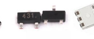
Marking of SMD components
SMD components are increasingly used in industrial and consumer devices. Surface mounting has improved performance over conventional mounting by reducing the size of the components and therefore the size of the traces. All these factors reduced parasitic inductance and capacitance in electrical circuits.
| Code | Resistance |
| 101 | 100 Ohm |
| 471 | 470 Ohm |
| 102 | 1 kOhm |
| 122 | 1.2 kOhm |
| 103 | 10 kOhm |
| 123 | 12 kOhm |
| 104 | 100 kOhm |
| 124 | 120 kOhm |
| 474 | 470 kOhm |
Useful information: how to test a transistor using a multimeter.
Marking of imported SMDs
Marking of imported SMD transistors occurs mainly according to several accepted systems. One of them is the JEDEC semiconductor device marking system. According to it, the first element is the number of n-junctions, the second element is the type rating, the third is the serial number, and if there is a fourth, modifications.
The second common labeling system is European. According to it, the designation of SMD transistors occurs according to the following scheme: the first element is the type of source material, the second is the subclass of the device, the third element is the definition of the application of this element, the fourth and fifth are the main specification of the element.
The third popular marking system is Japanese. This system combined the two previous ones. According to it, the first element is the class of the device, the second is the letter S, placed on all semiconductors, the third is the type of device by design, the fourth is the registration number, the fifth is the modification index, the sixth is the (optional) relation to special standards.
It will be interesting➡ SMD transistors
Whatever you get your hands on, to fully identify this element, you should use marking tables and use them to determine all the characteristics of this element. According to experts, the ratio between the production of ERE in conventional and SMD versions should approach 30:70. Many radio amateurs are already beginning to successfully master the use of SMD in their designs.
What are the labeling standards?
The markings that are applied to the body of SMD elements, as a rule, differ from their brand names. The reason is trivial - lack of space due to the miniature size of the case. The problem is especially relevant for electronic electronic devices, which are placed in packages with six or fewer leads.
These are miniature diodes, transistors, voltage stabilizers, amplifiers, etc. To figure out “what is what”, a real examination is required, because it is very difficult to identify the type of ERE using one marking code without additional information. More than 20 years have passed since the appearance of the first SMD devices.
Despite all attempts at standardization, manufacturing companies are still stubbornly inventing new types of SMD cases and haphazardly assigning marking codes to their elements.
Material on the topic: ringing a transistor with your own hands.
It’s not so bad that the applied symbols do not even closely resemble the name of the ERE; the worst thing is that there are cases of “plagiarism” when the same codes are assigned to functionally different devices from different companies.
| Type | Name of ERE | Foreign name |
| A1 | N-channel field effect transistor | Feld-Effect Transistor (FET), N-Channel |
| A2 | Double-gate N-channel field-effect transistor | Tetrode, Dual-Gate |
| A3 | Set of N-channel field effect transistors | Double MOSFET Transistor Array |
| B1 | Field-effect P-channel transistor | MOS, GaAs FET, P-Channel |
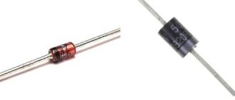
| D1 | One diode for wide application | General Purpose, Switching, PIN-Diode |
| D2 | Two widely used diodes | Dual Diodes |
| D3 | Three widely used diodes | Triple Diodes |
| D4 | Four widely used diodes | Bridge, Quad Diodes |
| E1 | One pulse diode | Rectifier Diode |
| E2 | Two pulse diodes | Dual |
| E3 | Three pulse diodes | Triple |
| E4 | Four pulse diodes | Quad |
| F1 | One Schottky diode | AF-, RF-Schottky Diode, Schottky Detector Diode |
| F2 | Two Schottky diodes | Dual |
| F3 | Three Schottky diodes | Triple |
| F4 | Four Schottky diodes | Quad |
| K1 | “Digital” NPN transistor | Digital Transistor NPN |
| K2 | A set of “digital” NPN transistors | Double Digital NPN Transistor Array |
| L1 | “Digital” PNP transistor | Digital Transistor PNP |
| L2 | A set of “digital” PNP transistors | Double Digital PNP Transistor Array |
| L3 | Set of “digital” transistors | PNP, NPN | Double Digital PNP-NPN Transistor Array |
| N1 | Bipolar LF transistor NPN (f < 400 MHz) | AF-Transistor NPN |
| N2 | Bipolar RF transistor NPN (f > 400 MHz) | RF Transistor NPN |
| N3 | High voltage NPN transistor (U > 150 V) | High-Voltage Transistor NPN |
| N4 | “Superbeta” NPN transistor (r“21e > 1000) | Darlington Transistor NPN |
| N5 | NPN transistor set | Double Transistor Array NPN |
| N6 | Low noise NPN transistor | Low-Noise Transistor NPN |
| 01 | Operational amplifier | Single Operational Amplifier |
| 02 | Comparator | Single Differential Comparator |
| P1 | Bipolar LF transistor PNP (f < 400 MHz) | AF-Transistor PNP |
| P2 | RF bipolar transistor PNP (f > 400 MHz) | RF Transistor PNP |
| P3 | High voltage PNP transistor (U > 150 V) | High-Voltage Transisnor PNP |
| P4 | “Superbeta” PNP transistor (p21e > 1000) | Darlington Transistor PNP |
| P5 | PNP Transistor Set | Double Transistor Array PNP |
| P6 | Set of transistors PNP, NPN | Double Transistor Array PNP-NPN |
| S1 | One suppressor | Transient Voltage Suppressor (TVS) |
| S2 | Two suppressors | Dual |
| T1 | Reference voltage source | “Bandgap”, 3-Terminal Voltage Reference |
| T2 | Voltage regulator | Voltage Regulator |
| T3 | Voltage detector | Voltage Detector |
| U1 | FET amplifier | GaAs Microwave Monolithic Integrated Circuit (MMIC) |
| U2 | Bipolar amplifier NPN | Si-MMIC NPN, Amplifier |
| U3 | Bipolar amplifier PNP | Si-MMIC PNP, Amplifier |
| V1 | One varicap (varactor) | Tuning Diode, Varactor |
| V2 | Two varicaps (varactors) | Dual |
| Z1 | One zener diode | Zener Diode |
It will be interesting➡ The principle of operation of the diode and its scope
A4 SMD MARKING
A guide to the coding of surface mount elements starting with 2 A4 characters. A brief description of the purpose and parameters (various zener diodes, stabilizers, microcontrollers, transistors, converters, varicaps and other chip parts). Standard designation options are indicated, but since new elements are constantly appearing, the compiled short guide is not entirely accurate and will be periodically updated. The entire table of SMD parts is available at the link
| code | Name | function | frame | manufacturer |
| A4 | 74AUP1Z04GS/G* | quartz driver | sot363/xson6 | NXP |
| A4 | BAV70/T/W/M | two RF diodes OK: 75 V/450 mA | sot23/sot416/sot883 | Nexperia |
| A4 | BAV70S | 2x dual RF diodes OK: 75 V/450 mA | sot363 | NXP |
| A4 | BAV70|W | two fast diodes OK: 70V/200 mA/6 ns | sot23|sot323 | Diotec |
| A4 | BC847CQB | npn: 45V/100 mA h21=420…800 automotive | dfn1110-3 | Nexperia |
| A4 | BZX884-B3V3 | Zener diode 250 mW: 3.3V | sod882 | NXP |
| A4 | KDZ36V | Zener diode 200 mW: 36V | usc | KEC |
| A4 | PESD5V0S4UF | 4x suppressor: 5.0 V | sot886 | NXP |
| A4 | PTVS6V5S1UR | suppressor 400W: 6.5 V | sod123w | NXP |
| A4x | HSMS-2804/-280F | two Schottky diodes with a common cathode | sot23/sot323 | Avago |
| A40 | OPA340NA | CMOS op-amp r2r i/o 6 V/µs | sot23-5 | T.I. |
| A40 | OPA363 | Op amp R2R I/O micropower powered from 1.8 V | sot23-6 | T.I. |
| A40A | OPA340EA | CMOS op-amp r2r i/o 6 V/µs | vssop8 | T.I. |
| A41 | 74AHC2G241DC/GD | two-gate tst buffer | vssop8/xson8 | NXP |
| A41 | OPA364 | Op amp R2R I/O micropower powered from 1.8 V | sot23-5 | T.I. |
| A44 | OPA(2)244A | Op-amp (dual) micropower | sot23-5(msop-8) | T.I. |
| A45A | LM8261M5 | Op amp RRIO with powerful output | sot23-6 | T.I. |
| A46 | BAR46A | 2 OA Schottky diodes: 100 V/150 mA | sot23 | STM |
| A46 | LM8262MM | dual op-amp RRIO with powerful output | msop8 | T.I. |
| A47A | LMV711M6 | universal op-amp RRIO with resolution, 5 V/µs | sot23-6 | T.I. |
| A48 | OPA348AI | CMOS op-amp R2R I/O 1 MHz ind | sot23-5 | T.I. |
| A48 | LMV301MG | CMOS op-amp RRO Upit=1.8 V | sc70-5 | T.I. |
| A48A | LMV710M5 | universal op-amp R2R I/O, 5 V/µs | sot23-5 | T.I. |
| A49 | OPA349NA | micro-power CMOS op-amp R2R I/O 70 kHz | sot23-5 | T.I. |
| A4A | AD8541RT | Op amp precision | sot23-5 | ADI |
| A4K | AD8541KS | Op amp precision | sc70-8 | ADI |
| A4p | BAV70/T/W/M | two RF diodes OK: 75V/450 mA | sot23/sot323/sot883 | NXP |
| A4p | BAV70S | 2x dual RF diodes OK: 75V/450 mA | sot363 | NXP |
| A4s | BAV70/T/U/W | 2 fast diodes OK: 70V/215 mA | sot23/sc75/sc74/sot323 | Infineon |
| A4s | BAV70S | 2x dual fast diodes OK: 70V/215 mA | sot363 | Infineon |
| A4t | BAV70/T/W/M | two RF diodes OK: 75 V/450 mA | sot23/sot416/sot883 | NXP |
| A4t | BAV70S | 2x dual RF diodes OK: 75V/450 mA | sot363 | NXP |
| A4W | BAV70/T/W | two RF diodes OK: 75 V/450 mA | sot23/sot416/sot883 | NXP |
| A4W | BAV70S | 2x dual RF diodes OK: 75V/450 mA | sot363 | NXP |
When deciphering the designation, keep in mind that when marking planar components, the symbols “O” and “0” (zero and round letter) are considered the same. And here you can see different types of housing sizes for SMD parts
- SM SMD MARKING
- VI SMD MARKING
- VJ SMD MARKING
- VK SMD MARKING
Foreign SMD marking
The table below summarizes information on the marking codes of semiconductor devices from leading foreign companies. For the sake of compactness, this reference material does not include duplicate devices that have the same markings and the same name, but are produced by different manufacturers. For example, the BFR93A transistor is produced not only by Siemens, but also by Philips Semiconductors and Temic Telefunken.
Table of marking codes for semiconductor devices from leading foreign companies.
Among the 18 presented types of housings, the most common is SOT-23 - Small Outline Transistor. It is quite old and has survived several attempts at standardization.
Above were the design tolerance standards that guide different companies. Despite the recommendations of IEC, JEDEC, EIAJ, it is impossible to find two absolutely identical standard sizes in Table 1.
Interesting read: what are bipolar transistors.
The information provided will be of assistance to specialists repairing imported radio equipment. Knowing the marking code and dimensions of the electrical electronics, you can determine the type of element and manufacturer, and then use catalogs to find electrical parameters and select a possible replacement.
In addition, many companies use their own housing names. It should be noted that domestic types of cases, such as KT-46 - an analogue of SOT-23, KT-47 - an analogue of SOT-89, KT-48 - an analogue of SOT-143, were approved back in 1988.
Several dozen varieties of domestic SMD elements released during this time are marked, as a rule, only on the packaging container; KT3130A9 transistors are also marked with multi-colored marks on the case. The most recent types of packages are SOT-23/5 (or, in other words, SOT-23-5) and SOT-89/5 (SOT-89-5), where the number “5” indicates the number of pins.
It is difficult to call such designations successful, since they can easily be confused with three-pin SOT-23 and SOT-89. Continuing the topic, we note that there have been reports of a subminiature 5-pin package SOT-323-5 (JEDEC specification), in which Texas Instruments plans to produce PicoGate Logic logic elements of the ACH1G and ACHT1G series.
Of all the cases, the relatively large SOT-223 can be called “random”. Usually, if not all, then most of the numbers and letters of the name of the ERE are placed on it, by which its type is clearly determined. Despite the miniature size of SMD elements, their parameters, including power dissipation, are not much different from their case counterparts.
For information, the reference data for transistors in the SOT-23 package indicates the maximum permissible power of 0.25-0.4 W, in the SOT-89 package - 0.5-0.8 W, in the SOT-223 package - 1-2 Tue.
The element marking code can be numeric, alphabetic or alphanumeric. The number of code characters is from 1 to 4, while the full name of the ERE contains 5-14 characters.
Material on the topic: how to test a field-effect transistor.
The longest names are used:
- American company Motorola,
- Japanese Seiko Instruments
- Taiwanese Pan Jit.
| Code | Type | ERE | Firm | Rice. | Code | Type | ERE | Firm | Rice. |
| 7E | MUN5215DW1T1 | K2 | M.O. | 2Q | |||||
| 11 | MUN5311DW1T1 | L3 | M.O. | 2Q | 7F | MUN5216DW1T1 | K2 | M.O. | 2Q |
| 12 | MUN5312DW1T1 | L3 | M.O. | 2Q | 7G | MUN5230DW1T1 | K2 | M.O. | 2Q |
| 12 | INA-12063 | U2 | HP | 2Q | 7H | MUN5231DW1T1 | K2 | M.O. | 2Q |
| 13 | MUN5313DW1T1 | L3 | M.O. | 2Q | 7J | MUN5232DW1T1 | K2 | M.O. | 2Q |
| 14 | MUN5314DW1T1 | L3 | M.O. | 2Q | 7K | MUN5233DW1T1 | K2 | M.O. | 2Q |
| 15 | MUN5315DW1T1 | L3 | M.O. | 2Q | 7L | MUN5234DW1T1 | K2 | M.O. | 2Q |
| 16 | MUN5316DW1T1 | L3 | M.O. | 2Q | 7M | MUN5235DW1T1 | K2 | M.O. | 2Q |
| 1C | BC847S | N5 | S.I. | 2Q | 81 | MGA-81563 | U1 | HP | 2Q |
| 1P | BC847PN | P6 | S.I. | 2Q | 82 | INA-82563 | U1 | HP | 2Q |
| 31 | MUN5331DW1T1 | L3 | M.O. | 2Q | 86 | INA-86563 | U1 | HP | 2Q |
| 32 | MUN5332DW1T1 | L3 | M.O. | 2Q | 87 | INA-87563 | U1 | HP | 2Q |
| 33 | MUN5333DW1T1 | L3 | M.O. | 2Q | 91 | IAM-91563 | U1 | HP | 2Q |
| 34 | MUN5334DW1T1 | L3 | M.O. | 2Q | A2 | MBT3906DW1T1 | P5 | M.O. | 2Q |
| 35 | MUN5335DW1T1 | L3 | M.O. | 2Q | A3 | MBT3906DW9T1 | P5 | M.O. | 2Q |
| 36 | ATF-36163 | A1 | HP | 2Q | A4 | BAV70S | E4 | S.I. | 2Q |
| 3C | BC857S | P5 | S.I. | 2Q | E6 | MDC5001T1 | U3 | M.O. | 2Q |
| 3X | MUN5330DW1T1 | L3 | M.O. | 2Q | H5 | MBD770DWT1 | F2 | M.O. | 2Q |
| 46 | MBT3946DW1T1 | P6 | M.O. | 2Q | II | AT-32063 | N2 | HP | 2Q |
| 51 | INA-51063 | U2 | HP | 2Q | M1 | CMY200 | U1 | S.I. | 2R |
| 52 | INA-52063 | U2 | HP | 2Q | M4 | MBD110DWT1 | F2 | M.O. | Q |
| 54 | INA-54063 | U2 | HP | 2Q | M6 | MBF4416DW1T1 | A3 | M.O. | 2Q |
| 6A | MUN5111DW1T1 | L2 | M.O. | 2Q | M.A. | MBT3904DW1T1 | N5 | M.O. | 2Q |
| 6B | MUN5112DW1T1 | L2 | M.O. | 2Q | M.B. | MBT3904DW9T1 | N5 | M.O. | 2Q |
| 6C | MUN5113DW1T1 | L2 | M.O. | 2Q | M.C. | BFS17S | N5 | S.I. | 2Q |
| 6D | MBF5457DW1T1 | A3 | M.O. | 2Q | RE | BFS480 | N5 | S.I. | 2Q |
| 6D | MUN5114DW1T1 | L2 | M.O. | 2Q | RF | BFS481 | N5 | S.I. | 2Q |
| 6E | MUN5115DW1T1 | L2 | M.O. | 2Q | RG | BFS482 | N5 | S.I. | 2Q |
| 6F | MUN5116DW1T1 | L2 | M.O. | 2Q | RH | BFS483 | N5 | S.I. | 2Q |
| 6G | MUN5130DW1T1 | L2 | M.O. | 2Q | T4 | MBD330DWT1 | F2 | M.O. | 2Q |
| 6H | MUN5131DW1T1 | L2 | M.O. | 2Q | W1 | BCR10PN | L3 | S.I. | 2Q |
| 6J | MUN5132DW1T1 | L2 | M.O. | 2Q | W.C. | BCR133S | K2 | S.I. | 2Q |
| 6K | MUN5133DW1T1 | L2 | M.O. | 2Q | W.F. | BCR08PN | L3 | S.I. | 2Q |
| 6L | MUN5134DW1T1 | L2 | M.O. | 2Q | W.K. | BCR119S | K2 | S.I. | 2Q |
| 6M | MUN5135DW1T1 | L2 | M.O. | 2Q | W.M. | BCR183S | K2 | S.I. | 2Q |
| 7A | MUN5211DW1T1 | K2 | M.O. | 2Q | W.P. | BCR22PN | L3 | S.I. | 2Q |
| 7B | MUN5212DW1T1 | K2 | M.O. | 2Q | Y2 | CLY2 | A1 | S.I. | 2R |
| 7C | MUN5213DW1T1 | K2 | M.O. | 2Q | 6s | CGY60 | U1 | S.I. | 2R |
| 7D | MUN5214DW1T1 | K2 | M.O. | 2Q | Y7s | CGY62 | U1 | S.I. | 2R |
It will be interesting➡ What are field-effect transistors?
Marking of SMD transistors
An article for determining the type of transistor by the designation on the case, as well as its conventional analogue.
| Designation on the body | Transistor type | Conditional analogue |
| 15 | MMBT3960 | 2N3960 |
| 1A | BC846A | BC546A |
| 1B | BC846B | BC546B |
| 1C | MMBTA20 | MPSA20 |
| 1D | BC846 | — |
| 1E | BC847A | BC547A |
| 1F | BC847B | BC547B |
| 1G | BC847C | BC547C |
| 1H | BC847 | — |
| 1J | BC848A | BC548A |
| 1K | BC848B | BC548B |
| 1L | BC848C | BC548C |
| 1M | BC848 | — |
| 1P | FMMT2222A | 2N2222A |
| 1T | MMBT3960A | 2N3960A |
| 1X | MMBT930 | — |
| 1Y | MMBT3903 | 2N3903 |
| 2A | FMMT3906 | 2N3906 |
| 2B | BC849B | BC549B |
| 2C | BC849C | BC549C/BC109C/MMBTA70 |
| 2E | FMMTA93 | — |
| 2F | BC850B | BC550B |
| 2G | BC850C | BC550C |
| 2J | MMBT3640 | 2N3640 |
| 2K | MMBT8598 | — |
| 2M | MMBT404 | — |
| 2N | MMBT404A | — |
| 2T | MMBT4403 | 2N4403 |
| 2W | MMBT8599 | — |
| 2X | MMBT4401 | 2N4401 |
| 3A | BC856A | BC556A |
| 3B | BC856B | BC556B |
| 3D | BC856 | — |
| 3E | BC857A | BC557A |
| 3F | BC857B | BC557B |
| 3G | BC857C | BC557C |
| 3J | BC858A | BC558A |
| 3K | BC858B | BC558B |
| 3L | BC858C | BC558C |
| 3S | MMBT5551 | — |
| 4A | BC859A | BC559A |
| 4B | BC859B | BC559B |
| 4C | BC859C | BC559C |
| 4E | BC860A | BC560A |
| 4F | BC860B | BC560B |
| 4G | BC860C | BC560C |
| 4J | FMMT38A | — |
| 449 | FMMT449 | — |
| 489 | FMMT489 | — |
| 491 | FMMT491 | — |
| 493 | FMMT493 | — |
| 5A | BC807-16 | BC327-16 |
| 5B | BC807-25 | BC327-25 |
| 5C | BC807-40 | BC327-40 |
| 5E | BC808-16 | BC328-16 |
| 5F | BC808-25 | BC328-25 |
| 5G | BC808-40 | BC328-40 |
| 549 | FMMT549 | — |
| 589 | FMMT589 | — |
| 591 | FMMT591 | — |
| 593 | FMMT593 | — |
| 6A | BC817-16 | BC337-16 |
| 6B | BC817-25 | BC337-25 |
| 6C | BC817-40 | BC337-40 |
| 6E | BC818-16 | BC338-16 |
| 6F | BC818-25 | BC338-25 |
| 6G | BC818-40 | BC338-40 |
| 9 | BC849BLT1 | — |
| A.A. | BCW60A | BC636/BCW60A |
| AB | BCW60B | — |
| A.C. | BCW60C | BC548B |
| AD | BCW60D | — |
| A.E. | BCX52 | — |
| A.G. | BCX70G | — |
| A.H. | BCX70H | — |
| A.J. | BCX70J | — |
| A.K. | BCX70K | — |
| AL | MMBTA55 | — |
| A.M. | BSS64 | 2N3638 |
| AS1 | BST50 | BSR50 |
| B2 | BSV52 | 2N2369A |
| B.A. | BCW61A | BC635 |
| BB | BCW61B | — |
| B.C. | BCW61C | — |
| BD | BCW61D | — |
| BE | BCX55 | — |
| B.G. | BCX71G | — |
| B.H. | BCX71H | BC639 |
| B.J. | BCX71J | — |
| B.K. | BCX71K | — |
| BN | MMBT3638A | 2N3638A |
| BR2 | BSR31 | 2N4031 |
| C1 | BCW29 | — |
| C2 | BCW30 | BC178B/BC558B |
| C5 | MMBA811C5 | — |
| C6 | MMBA811C6 | — |
| C7 | BCF29 | — |
| C8 | BCF30 | — |
| C.E. | BSS79B | — |
| CEC | BC869 | BC369 |
| CF | BSS79C | — |
| CH | BSS82B/BSS80B | — |
| C.J. | BSS80C | — |
| C.M. | BSS82C | — |
| D1 | BCW31 | BC108A / BC548A |
| D2 | BCW32 | BC108A / BC548A |
| D3 | BCW33 | BC108C/BC548C |
| D6 | MMBC1622D6 | — |
| D7 | BCF32 | — |
| D8 | BCF33 | BC549C/BCY58/MMBC1622D8 |
| D.A. | BCW67A | — |
| D.B. | BCW67B | — |
| DC | BCW67C | — |
| DE | BFN18 | — |
| DF | BCW68F | — |
| DG | BCW68G | — |
| D.H. | BCW68H | — |
| E1 | BFS17 | BFY90/BFW92 |
| E.A. | BCW65A | — |
| E.B. | BCW65B | — |
| E.C. | BCW65C | — |
| ED | BCW65C | — |
| E.F. | BCW66F | — |
| E.G. | BCW66G | — |
| E.H. | BCW66H | — |
| F1 | MMBC1009F1 | — |
| F3 | MMBC1009F3 | — |
| F.A. | BFQ17 | BFW16A |
| FD | BCV26 | MPSA64 |
| F.E. | BCV46 | MPSA77 |
| FF | BCV27 | MPSA14 |
| FG | BCV47 | MPSA27 |
| GF | BFR92P | — |
| H1 | BCW69 | — |
| H2 | BCW70 | BC557B |
| H3 | BCW89 | — |
| H7 | BCF70 | — |
| K1 | BCW71 | BC547A |
| K2 | BCW72 | BC547B |
| K3 | BCW81 | — |
| K4 | BCW71R | — |
| K7 | BCV71 | — |
| K8 | BCV72 | — |
| K9 | BCF81 | — |
| L1 | BSS65 | — |
| L2 | BSS70 | — |
| L3 | MMBC1323L3 | — |
| L4 | MMBC1623L4 | — |
| L5 | MMBC1623L5 | — |
| L6 | MMBC1623L6 | — |
| L7 | MMBC1623L7 | — |
| M3 | MMBA812M3 | — |
| M4 | MMBA812M4 | — |
| M5 | MMBA812M5 | — |
| M6 | BSR58/MMBA812M6 | 2N4858 |
| M7 | MMBA812M7 | — |
| O2 | BST82 | — |
| P1 | BFR92 | BFR90 |
| P2 | BFR92A | BFR90 |
| P5 | FMMT2369A | 2N2369A |
| Q3 | MMBC1321Q3 | — |
| Q4 | MMBC1321Q4 | — |
| Q5 | MMBC1321Q5 | — |
| R1 | BFR93 | BFR91 |
| R2 | BFR93A | BFR91 |
| S1A | SMBT3904 | — |
| S1D | SMBTA42 | — |
| S2 | MMBA813S2 | — |
| S2A | SMBT3906 | — |
| S2D | SMBTA92 | — |
| S2F | SMBT2907A | — |
| S3 | MMBA813S3 | — |
| S4 | MMBA813S4 | — |
| T1 | BCX17 | BC327 |
| T2 | BCX18 | — |
| T7 | BSR15 | 2N2907A |
| T8 | BSR16 | 2N2907A |
| U1 | BCX19 | BC337 |
| U2 | BCX20 | — |
| U7 | BSR13 | 2N2222A |
| U8 | BSR14 | 2N2222A |
| U9 | BSR17 | — |
| U92 | BSR17A | 2N3904 |
| Z2V | FMMTA64 | — |
| ZD | MMBT4125 | 2N4125 |