The designation system for modern types of transistors is established by the industry standard OST 11336.919-81.
The notation system is based on an alphanumeric code. The first element (number or letter) indicates the source semiconductor material on which the transistor is made, the second element (letter) determines the subclass (or group) of transistors, the third (number) indicates the main functionality of the transistor, the fourth (number) indicates the serial number of the development technological type of transistor, fifth (letter) - conditionally determines the classification according to the parameters of transistors manufactured using a single technology.
Bipolar (ordinary) transistor
Bipolar transistors are the most widely used. We'll probably start with them. In a simplified form, a bipolar transistor is a semiconductor wafer with three (as in a layer cake) alternating regions of different electrical conductivity (Fig. 1), which form two p-n junctions.
The two extreme regions have electrical conductivity of one type, the middle one has electrical conductivity of another type. Each area has its own contact pin. If hole electrical conductivity predominates in the outer regions, and electronic conductivity in the middle (Fig. 1, a), then such a device is called a transistor of the p - n - p structure . A transistor with an n-p-n structure, on the contrary , has regions with electronic conductivity along the edges, and between them there is a region with hole conductivity (Fig. 1, b).
Rice. 1 Schematic structure and graphic designation on the diagrams of transistors of the p - n - p and n - p - n structure.
Device and structure.
If you mentally cover any of the extreme areas of the transistors shown schematically in (Fig. 1). What happened? The remaining two areas are nothing more than a planar diode. If you cover the other extreme area, you will also get a diode. This means that a transistor can be imagined as two planar diodes with one common area, connected towards each other.
The general (middle) region of the transistor is called the base, one extreme region is the emitter, and the second extreme region is the collector.
These are the three electrodes of the transistor. During operation, the emitter introduces (emits) holes (in the p-n-p structure) or electrons (in the n-p-n structure) into the base, the collector collects these electrical charges introduced into the base by the emitter.
The difference in the designations of transistors of different structures in the diagrams lies only in the direction of the emitter arrow: in p - n - p transistors it faces towards the base, and in n - p - n - away from the base.
Electron-hole transitions in a transistor can be obtained in the same way as in planar diodes. For example, to make a transistor with a p-n-p structure, they take a thin plate of germanium with electronic conductivity and fuse pieces of indium onto its surface. Indium atoms diffuse (penetrate) into the body of the plate, forming two p-type regions in it - the emitter and the collector, and between them there remains a very thin (several microns) layer of n-type semiconductor - the base. Transistors manufactured using this technology are called alloy.
Remember the names of the p-n junctions of the transistor: between the collector and the base - collector, between the emitter and base - emitter.
The schematic structure and design of the alloy transistor is shown in (Fig. 2).
Manufacturing of transistors.
The device is assembled on a metal disk with a diameter of less than 10 mm. A crystal holder, which is the internal lead of the base, is welded to the top of this disk, and its outer wire lead is welded to the bottom. The internal terminals of the collector and emitter are welded to wires, which are soldered into glass insulators and serve as the external terminals of these electrodes. The all-metal cap protects the device from mechanical damage and the influence of light. This is how the most common low-power low-frequency transistors of the MP39, MP40, MP41, MP42 series and their varieties are designed. The letter (M) in the designation indicates that the body of the device is cold-welded, the letter (P) is the initial letter of the words “planar”, and the numbers are the serial serial numbers of the devices. At the end of the designation there may be the letters A, B, C (for example, MP39B), indicating the difference in the parameters of this series. There are other manufacturing methods, for example, diffusion alloy (Fig. 3). The collector of a transistor made using this technology is the wafer of the original semiconductor. Two small balls of impurity elements are fused onto the surface of the plate very close to one another. During heating to a strictly defined temperature, impurity elements diffuse into the semiconductor wafer. In this case, one ball (right in Fig. 3) forms a thin base region in the collector, and the second (left in Fig. 3) forms an emitter region.
Rice. 2 - Design and construction of a transistor alloyed on the left and diffusionally alloyed on the right of the p - n - p structure.
As a result, two p-n junctions are obtained in the wafer of the original semiconductor, forming a transistor of the p-n-p structure. Using this technology, in particular, the most widespread low-power high-frequency transistors of the P401-P403, P422, P423, GT308 series are manufactured. Currently, there is a designation system in place, according to which commercially produced devices have designations consisting of four elements, for example: GT109A, KT315V, GT403I.
- The first element of this designation system - the letter G, K or A (or the number 1, 2 and 3) - characterizes the semiconductor material and the temperature conditions of the device. The letter G (or number 1) is assigned to germanium transistors, the letter K (or number 2) to silicon, the letter A (or number 3) to transistors whose semiconductor material is gallium arsenide. A number instead of a letter indicates that this transistor can operate at elevated temperatures (germanium - above 4-60°C, silicon - above +85°C).
- The second element is the letter T, the initial letter of the word “transistor.”
- The third element - a three-digit number from 101 to 999 - indicates the serial number of development and the purpose of the device. This number is assigned to the transistor according to the criteria given in the table.
- The fourth element of the designation is a letter indicating the type of device in this series.
Here are some examples of decoding notations using this system:
GT109A - germanium low-power low-frequency transistor, type A;
GT404G - germanium medium-power low-frequency transistor, variety G;
KTZ15V - silicon low-power high-frequency transistor, type B.
Application of transistors
Along with this system, the previous designation system continues to operate, for example P27, P401, P213, MP39, etc. This is explained by the fact that these or similar transistors were developed before the introduction of modern labeling of semiconductor devices. The appearance of some bipolar transistors most widely used by radio amateurs is shown in (Fig. 4). The low-power low-frequency transistor GT109 (p-n-p structure) has a diameter of only 3.4 mm. Transistors of this series are designed for miniature radio broadcast receivers. They are also used in hearing aids, electronic medical devices, etc.
The diameter of GT309 transistors (p - n - p) is 7.4 mm. Such transistors are used in various small-sized electronic devices to amplify and generate high-frequency oscillations.
Transistors KTZ15 (n - p - n) are produced in plastic cases. These low-power devices are designed to amplify and generate high frequency oscillations. Transistors MP39 - MP42 (p - n - p) are the most popular among low-power low-frequency transistors. Similar ones look exactly the same, but the structures are n - p - n, transistors MP35 - MP38. The case diameter of any of these transistors is 11.5 mm. They are most widely used in audio amplifiers.
This is also what low-power high-frequency p-n-p transistors of the P401 - P403, P416, P423 series look like, used to amplify high-frequency signals in both industrial and amateur radio broadcast receivers. Transistor GT402 (p - n - p) is a representative of low-frequency medium-power transistors. Its “twin” GT404 has the same design, but it has a structure (n - p - n). They are usually used in pairs in cascades for amplifying the power of audio frequency oscillations.
Transistor P213 (germanium p-n-p structure) is one of the powerful low-frequency transistors widely used in the final stages of audio amplifiers. The diameter of this, as well as similar transistors P214 - P216 and some others, is 24 mm. Such transistors are mounted on chassis or panels using flanges. During operation, they heat up, so they are usually placed on special heat sinks that increase the cooling surface.
KT904 is a high-power ultra-high-frequency silicon n-p-n transistor. The case is metal-ceramic with rigid leads and an M5 screw, with which the transistor is mounted on a heat-conducting radiator. The function of a radiator can be performed by a massive metal plate or a metal chassis of a radio device. The height of the transistor together with the leads and mounting screw is slightly more than 20 mm. Transistors of this series are intended for generators and power amplifiers of radio equipment operating at frequencies above 100 MHz, for example, the VHF band.
Rice. 4 Appearance of some transistors.
I advise you to watch the educational film:
Switching circuits and main parameters of bipolar transistors
So, a bipolar transistor, regardless of its structure, is a three-electrode device. Its electrodes are emitter, collector and base. To use a transistor as a voltage, current or power amplifier, the input signal that needs to be amplified can be applied to any two electrodes and the amplified signal can be removed from two electrodes. In this case, one of the electrodes will necessarily be common. It is this that determines the name of the method of switching on the transistor: according to a common emitter (CE) circuit, according to a common collector (OC) circuit, according to a common base (CB) circuit.
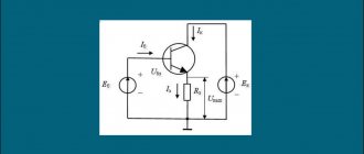
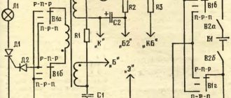
- The inclusion of a pn-p transistor according to the OE circuit is shown in (Fig. 5, a). The power source voltage at the collector V is supplied through a resistor Rк, which is a load, and to the emitter through a common “grounded” conductor, indicated in the diagrams with a special sign. Input signal through coupling capacitor Csv. is supplied to the base and emitter terminals, i.e. to the base-emitter section, and the amplified signal is removed from the emitter and collector terminals. The emitter, therefore, with this connection is common to the input and output circuits. A transistor, according to a circuit with an OE, depending on its amplification properties, can provide a 10-200-fold amplification of the signal in voltage and a 20-100-fold amplification of the signal in current. This method of switching on according to the OE circuit is the most popular among radio amateurs. A significant drawback of the amplifier stage connected according to this circuit is its relatively low input resistance - only 500-1000 Ohms, which complicates the matching of amplifier stages whose transistors are connected according to the same circuit. This is explained by the fact that in this case the emitter p-n junction of the transistor is switched on in direct mode, i.e. throughput direction. And the resistance of the throughput junction, which depends on the voltage applied to it, is always small. As for the output resistance of such a stage, it is quite large (2-20 kOhm) and depends on the load resistance Rk and amplifying properties.
- Switching on the device in the OK diagram is shown in (Fig. 5, b). The input signal is supplied to the base and emitter through the emitter resistor Re, which is part of the collector circuit. The output signal is also removed from the same resistor, which acts as a transistor load. Thus, this section of the collector circuit is common to the input and output circuits, which is why the name of the method of turning on the transistor is OK. A cascade with a semiconductor connected according to this circuit gives a voltage gain of less than unity. The current gain is approximately the same as if the transistor were connected according to the OE circuit. But the input resistance of such a cascade can be 10 - 500 kOhm, which is in good agreement with the high output resistance of the cascade on a transistor connected according to the OE circuit. Essentially, the cascade does not provide voltage gain, but only, as it were, repeats the signal supplied to it. Therefore, transistors connected according to this circuit are also called emitter followers . Why emitter? Because the output voltage at the emitter almost completely matches the input voltage. Why doesn't the cascade increase the voltage? Let's mentally connect the base circuit with a resistor to the lower (according to the diagram) terminal of the emitter resistor Re, as shown in (Fig. 5, b) with dashed lines. This resistor is the equivalent of the internal resistance of the input signal source Rin, such as a microphone or pickup. Thus, the emitter circuit is connected through the resistor Rin. with base. When a signal voltage is applied to the input of the amplifier, an amplified signal voltage is released across the resistor Re, which is the load of the transistor, which is released through the resistor Rin. turns out to be applied to the base in antiphase. In this case, a very strong negative feedback arises between the emitter and base circuits, negating the gain of the cascade. This is by voltage. And in terms of amplification current, the result is the same as when the transistor is turned on according to a circuit with an OE.
- Now about turning on the transistor according to the circuit with OB (Fig. 5, c). In this case, the base is grounded through the AC capacitor Sb, i.e., connected to a common power conductor. Input signal through capacitor Csv. is supplied to the emitter and base, and the amplified signal is removed from the collector and from the grounded base. The base is thus the common electrode of the input and output circuits of the cascade. Such a cascade gives a current gain of less than unity, and a voltage gain that is the same as a transistor connected according to a circuit with an OE (10 - 200). Due to the very low input resistance, BC exceeding several tens (30-100) Ohms, turning on the transistor according to the OB circuit is used mainly in generators of electrical oscillations, in supergenerative cascades, used, for example, in radio control equipment for models.
Most often, as I already said, circuits are used that include a transistor with an OE, less often with an OK one. But these are only ways of inclusion. And the operating mode of a transistor as an amplifier is determined by the voltages on its electrodes, currents in its circuits and, of course, the parameters of the transistor itself. The quality and amplifying properties of bipolar transistors are assessed by several electrical parameters, which are measured using special instruments. From a practical point of view, you should be primarily interested in three main parameters: the reverse collector current Ikbo , the static current transfer coefficient h213 (read as: ash two one e) and the cutoff frequency of the current transfer coefficient Fgr.
- The reverse collector current Ikbo is an uncontrolled current through the collector p-n junction created by the minority current carriers of the transistor. It characterizes the quality of the transistor: the smaller the numerical value of the Ikbo parameter, the higher the quality. For low-power low-frequency transistors, for example, the MP39 - MP42 series, Ikbo should not exceed 30 μA, and for low-power high-frequency transistors 5 μA. Transistors with large values of Ikbo are unstable in operation.
- The static current transfer coefficient h21e characterizes the amplification properties of the transistor. It is called static because this parameter is measured at constant voltages on its electrodes and constant currents in its circuits. The letter “E” in this expression indicates that during the measurement the semiconductor is switched on according to the OE circuit. The coefficient h21e is characterized by the ratio of the direct collector current to the constant base current at a given constant reverse collector-emitter voltage and emitter current. The greater the numerical value of the coefficient h21e, the greater the signal amplification this device can provide.
- The cutoff frequency of the current transfer coefficient Fgr, expressed in kilohertz or megahertz, allows us to judge the possibility of using a transistor to amplify oscillations of certain frequencies. The cutoff frequency Fgr of transistor MP39 is, for example, 500 kHz, and transistors P401 - P403 is more than 30 MHz. In practice, transistors are used to amplify frequencies much lower than the limiting ones, since with increasing frequency the coefficient h21e decreases.
When designing radio engineering devices, it is necessary to take into account such parameters as the maximum permissible collector-emitter voltage Uke max, the maximum permissible collector current Ik.max, as well as the maximum permissible dissipated power of the collector Pk.max - power converted into heat.
PRO-ELECTRON (system developed in Europe)
The marking of devices from European manufacturers is somewhat different. The code with which the foreign transistor is marked is a combination of the symbol:
- The symbol number one indicates the material from which the device is made: A – germanium, B – silicon, C – gallium arsenide, R – cadmium sulfide;
- The second symbol indicates the type of transistor: C – low-power device with low frequency; D – powerful element with low frequency; F – low power device with a high frequency level; G – two or more elements are present in one case at the same time; L – device with high power and frequency; S – low-power device with switching function; U – high power switch transistor;
- The third character indicates the product series number: general use products are marked with numbers from 100 to 999; in the case when a letter is written before the digital value, this indicates that this part is manufactured for use in industry or specialized use.
Moreover, the general encoding is sometimes supplemented with a modification symbol. Only the manufacturer himself can determine it.
Field-effect transistor
In this semiconductor device, the operating current is controlled not by the current in the input (base) circuit, as in a bipolar transistor, but by the influence of an electric field . Hence the name “field” . The schematic structure and design of a field-effect transistor with a p-n junction is shown in (Fig. 6). The basis of such a transistor is a silicon wafer with electrical conductivity of type n, in which there is a thin region with electrical conductivity of type p. The device plate is called a gate, and the region of type p in it is called a channel. On one side the channel ends with a source, on the other with a drain - also a region of type p, but with an increased concentration of holes. A p-n junction is created between the gate and the channel. Contact pins are made from gate, source and drain. If you connect the positive pole to the source and the negative pole to the drain (battery GB in Fig. 6), then a current will appear in the channel, created by the movement of holes from source to drain. This current, called the drain current Ic, depends not only on the voltage of this battery, but also on the voltage acting between the source and the gate (element G in Fig. 6).
And that's why. When a positive turn-off voltage is applied to the gate relative to the source, the depletion region of the p-n junction expands (shown by dashed lines in Fig. 6). As a result, the channel narrows, its resistance increases, which causes the drain current to decrease. As the positive gate voltage decreases, the depletion region of the p-n junction, on the contrary, narrows, the channel expands, and the current increases again. If a low-frequency or high-frequency signal is applied to the gate along with a positive bias voltage, a pulsating current will appear in the drain circuit, and an amplified signal voltage will appear at the load connected to this circuit. Thus, in a simplified form, field-effect transistors with a p-type channel are designed and operate, for example, KP102, KP103 (the letters K and P mean “silicon field-effect”). In principle, a field-effect transistor with a channel of type n is designed and operates in the same way. The gate of a transistor of such a structure has hole electrical conductivity, so a negative bias voltage must be applied to it relative to the source, and a positive voltage from the power source must be applied to the drain (also relative to the source). In a conventional graphical representation of a field-effect transistor with a channel of type n, the arrow on the gate line is directed towards the source, and not away from the source, as in the designation of a transistor with a channel of type p. A field-effect transistor is also a three-electrode device. Therefore, like a bipolar transistor, it can be included in an amplifier stage in three ways: using a common drain (OC) (CS) circuit (G) circuit . In amateur radio practice, mainly only the first two connection methods are used, which make it possible to use field-effect transistors with the greatest efficiency.
The amplifier stage on a field-effect transistor has a very large input resistance, measured in megaohms.
This allows high-frequency and low-frequency signals from sources with high internal resistance, such as a piezoceramic pickup, to be fed to its input without fear of distortion or deterioration in the gain of the input signal.
This is the main advantage of field-effect transistors compared to bipolar ones. The amplifying properties of a field-effect transistor are characterized by the slope of the characteristic S - the ratio of the change in drain current to the change in gate voltage during an AC short circuit at the output of the transistor connected according to the OI circuit. The numerical value of the parameter S is expressed in milliamperes per volt; for different transistors it can range from 0.1 - 0.2 to 10 - 15 mA/V and more. The greater the transconductance, the greater the signal amplification the transistor can provide.
Rice. 6 Design and graphical representation of a field-effect transistor with a type (p) channel.
Another parameter of the field-effect transistor is the cutoff voltage Uzi.ots . - This is the reverse voltage at the p-n junction of the gate-channel, at which the current through this junction decreases to zero. For various transistors, the cutoff voltage can range from 0.5 to 10 V. Much more can be said about field-effect transistors and their unique properties; I tried to talk about the most significant ones.
Marking of the year and month of manufacture of electronic components
According to GOST 25486-82 , in order to indicate the month and year of manufacture of the transistor and other electronic components, letters and numbers are used: the first value is the year, the second value is the month. As for devices manufactured abroad, a four-digit encoding is used to indicate the date of manufacture, where the first two are the year, the next are the model number.
Each year has its own letter:
Year Code
| 1986 | U |
| 1987 | V |
| 1988 | W |
| 1989 | X |
| 1990 | A |
| 1991 | B |
| 1992 | C |
| 1993 | D |
| 1994 | E |
| 1995 | F |
| 1996 | H |
| 1997 | I |
| 1998 | K |
| 1999 | L |
| 2000 | M |
| 2001 | N |
| 2002 | P |
| 2003 | R |
| 2004 | S |
| 2005 | T |
| 2006 | U |
| 2007 | V |
| 2008 | W |
| 2009 | X |
| 2010 | A |
| 2011 | B |
| 2012 | C |
| 2013 | D |
| 2014 | E |
| 2015 | F |
Month marking
Month Code
| January | 1 |
| February | 2 |
| March | 3 |
| April | 4 |
| May | 5 |
| June | 6 |
| July | 7 |
| August | 8 |
| September | 9 |
| October | O |
| November | N |
| December | D |
To indicate the month of issue, not only numbers, but also some letters are used: the months from January to September fully correspond to the numbers, the following ones correspond to the first letters of the name of the month.
Middle management
The main part is the simplest part of marking semiconductor elements. The first device of this type to be registered may be numbered “0001”, the next one “0002”, etc.
In practice, this doesn't quite work that way, and some transistor manufacturers start labeling their products with "100" rather than "001". But that doesn't matter.
A significant disadvantage of this marking method is the presence of more semiconductor devices than available numbers (3 or 4 digits).
For example, a device labeled "555" could be a popular timer integrated circuit (IC), a transistor with a European number type, and perhaps something else, such as another type of integrated circuit or optical device.
Thus, basic numeric markings are important but are not sufficient on their own to accurately identify an item.
To select the appropriate element, you must pay attention to other parts of the marking.
Checking the varistor for serviceability with a multimeter and without a tester
Causes of malfunction
How to check a fuse with a multimeter
Varistors are installed parallel to the protected circuit, and a fuse is placed in series with it. This is necessary so that when the varistor burns out, if the overvoltage pulse is too strong, the fuse will burn out, and not the tracks of the printed circuit board.
The only reason for the failure of a varistor is a sudden and strong voltage surge in the network. If the energy of this jump is greater than the varistor can dissipate, it will fail. The maximum energy dissipation depends on the dimensions of the component. They differ in diameter and thickness, that is, the larger they are, the more energy the varistor can dissipate.
Voltage surges can occur during accidents on power lines, during a thunderstorm, or when switching powerful devices, especially inductive loads.
Verification methods
Any repair of electronics and electrical equipment begins with an external inspection, and then proceeds to measurements. This approach allows you to localize most faults. To find a varistor on the board, look at the figure below - this is what varistors look like. Sometimes they can be confused with capacitors, but can be distinguished by their markings.
If the element is burnt out and the markings cannot be read, look at this information on the device diagram. On the board and in the diagram it can be designated by the letters RU. The conventional graphic symbol looks like this.
There are three ways to test a varistor quickly and easily:
- Visual inspection.
- Call. This can be done with a multimeter or any other device that has a continuity test function.
- Resistance measurement. This can be done with a high-range ohmmeter, multimeter or megger.
A varistor fails when a large or prolonged current passes through it. Then the energy is dissipated in the form of heat, and if its amount is greater than that determined by the design, the element burns out. The housing of these components is made of a hard dielectric material, such as ceramic or epoxy coating. Therefore, when it fails, the integrity of the outer coating is most often damaged.
You can visually check the varistor for functionality - there should be no cracks on it, as in the photo:
The next method is to check the varistor with a tester in continuity mode. This cannot be done in the circuit, because the dialing can work through parallel-connected elements. Therefore, you need to unsolder at least one of its legs from the board.
Important: you should not check the elements for serviceability without desoldering them from the board - this may give false readings from the measuring instruments. Since in the normal state (without voltage applied to the terminals) the resistance of the varistor is high, it should not ring through
The test is performed in both directions, that is, by swapping the multimeter probes twice
Since in the normal state (without voltage applied to the terminals) the resistance of the varistor is high, it should not ring through. The test is performed in both directions, that is, by swapping the multimeter probes twice.
On most multimeters, the continuity mode is combined with the diode testing mode. It can be found by the diode icon on the mode selector scale. If there is a sound indication sign next to it, it probably also has a dial tone.
Another way to test a varistor for breakdown with a multimeter is to measure the resistance. You need to set the device to the maximum measurement limit, in most devices this is 2 MOhms (megaohms, designated as 2M or 2000K). The resistance must be equal to infinity. In practice, it can be lower, within 1-2 MOhm.
Interesting! The same can be done with a megaohmmeter, but not everyone has one. It is worth noting that the voltage at the megohmmeter terminals should not exceed the classification voltage of the component being tested.
This ends the available methods for checking a varistor. This time, the multimeter will help the radio amateur find the faulty element, as in a large number of other cases. Although in practice a multimeter is not always needed in this matter, because the matter rarely goes beyond a visual inspection. Replace the burnt element with a new one, designed for voltage and with a diameter no less than the burnt one, otherwise it will burn out even faster than the previous one.
Japanese JIS system
Labeling standards developed in Japan are represented by letters and numbers in the amount of 5 pieces:
- The number 1 is the type of semiconductor transistor: 0 is the designation of a photodiode or phototransistor; 1 – diode designation; 2 – designation of the transistor;
- The letter symbol S is affixed to each item issued;
- The third marking element indicates the type of part: A – PNP with high frequency; B – PNP with low frequency; C—NPN with a high frequency level; D - NPN with low frequency level; N – single-junction; J - field-effect transistor with N-channel; K - field-effect transistor with P-channel;
- The number 4 is the series number in the range from 10 to 9999;
- The fifth symbol of the marking indicates a modification. Sometimes this symbol is missing.
There are situations when the encoding contains a 6th character - this is an additional letter N, M or S, which is responsible for the device’s compliance with certain standards. Labeling developed in Japan does not include color coding.
Sources
- https://habr.com/ru/post/133136/
- https://remont220.ru/osnovy-elektrotehniki/1098-tranzistor/
- https://remont220.ru/stati/595-shemy-vklyucheniya-tranzistorov/
- https://go-radio.ru/transistor.html
- https://tyt-sxemi.ru/tranzistor/
- https://tokar.guru/hochu-vse-znat/tranzistor-vidy-primenenie-i-principy-raboty.html
- https://raschet.info/cvetovaja-i-simvolno-cvetovaja-markirovka-tranzistorov/
- https://www.radiodetector.ru/markirovka-tranzistorov/
Tsokolevka
How to check how many amperes a generator produces with a multimeter
Medium and high power bipolar transistors have basically the same pinout, from left to right - emitter, collector, base. For low power transistors it is better to check
This is important because when determining performance, we will need this information
Appearance of a medium power bipolar transistor and its pinout
That is, if you need to determine whether a bipolar transistor is working or not, you need to look for its pinout. If you want to make sure or don’t know where the “face” is, then look for information in a reference book or type the “name” of your semiconductor device on your computer and add the word “datasheet”. This is a transliteration from English Datasheet, which translates as “technical data”. For this request, you will receive a list of characteristics of the device and its pinout.
Manufacturer
Most electronic components are marked according to the standard methods listed. But there are also exceptions. (Fig. 1).
Here the TIP prefix of this power transistor indicates that it is a plastic packaged power transistor from Texas Instruments. However, the manufacturer put the MOSPEC logo on the front, so the prefix became the second element of the marking.
This often occurs in the marking of integrated circuits, where the manufacturer adds its own coding to the standard type marking.
Fig.2. This integrated circuit has the designation "LM" as a prefix, indicating that it is a National Semiconductor product.
As a few examples: the prefixes "CA" and "MC" are used by KCA and Motorola, respectively. Due to the fact that the same element can be produced by different manufacturers and labeled differently, difficulties arise with identifying the elements.
Of course, the presence of several manufacturers on the market gives rise to competition, which, as a consequence, reduces prices for radioelements. This is good for us. On the other hand, each manufacturer adds something different to the labeling of elements, thereby making it difficult for us to identify them.
When browsing through an integrated circuit catalog, it's probably best to ignore the prefix and focus on the other two markings. Moreover, component suppliers often do not guarantee the supply of devices from specific manufacturers. If you order (say) MC1458CP. but they sent you CA1458E. or vice versa, there is no reason to worry. Both ICs are 1458 dual op amps and there is no practical difference between them. The MC1458CP is made by Motorola or Texas Instruments, and the CA1458E is made by RCA.