Imported amplifiers very often use a powerful complementary pair 2SA and 2SC. We will consider them later in a detailed study of the circuit of an amplifier stage with a common emitter. Capacitor Cp is a separating capacitor. If it is chosen correctly, the output voltage will be significantly higher than the input.
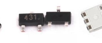
The current-voltage characteristic of the zener diode is shown in Fig. Bipolar transistors
Based on the operating frequency, transistors are divided into low-frequency - operating frequency not exceeding 3 MHz, mid-frequency - 3...30 MHz, high-frequency - over 30 MHz.
Figure 3.
The author of the article proposed regulating the rotation frequency of the commutator motor by changing the duration of the pulses in the control winding of the op-amp.
But the parameters of germanium transistors were unstable; their biggest drawback should be considered low operating temperature - no more
Although the transition layers are based on the same principle, the transistor is an asymmetrical device.
TRANSISTOR CONNECTION DIAGRAMS. EMITTER REPEATER [Radio Amateur TV 42]
What is a transistor?
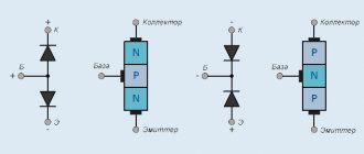
In its modern meaning, a transistor is a semiconductor radio element designed to change the parameters of an electric current and control it. A conventional semiconductor triode has three terminals: a base, which receives control signals, an emitter, and a collector. There are also high power composite transistors.
The size scale of semiconductor devices is striking - from several nanometers (unpackaged elements used in microcircuits) to centimeters in diameter for high-power transistors intended for power plants and industrial equipment. Reverse voltages of industrial triodes can reach up to 1000 V.
Basic operating principle
At rest, no current flows between the collector and emitter of a bipolar triode. Electric current is prevented by the resistance of the emitter junction, which arises as a result of the interaction of the layers. To turn on the transistor, you need to apply a small voltage to its base.
The figure shows a diagram explaining the working principle of a triode.
Principle of operation
By controlling the base currents, you can turn the device on and off. If an analog signal is applied to the base, it will change the amplitude of the output currents. In this case, the output signal will exactly repeat the oscillation frequency at the base electrode. In other words, the electrical signal received at the input will be amplified.
Thus, semiconductor triodes can operate in electronic switch mode or in input signal amplification mode.
The operation of the device in electronic key mode can be understood from Figure 3.
Triode in switch mode
Designation on diagrams
The generally accepted designation is “VT” or “Q”, followed by a positional index. For example, VT 3. On earlier diagrams you can find outdated designations: “T”, “PP” or “PT”. The transistor is depicted as symbolic lines indicating the corresponding electrodes, circled or not. The direction of current in the emitter is indicated by an arrow.
Figure 4 shows a ULF circuit in which transistors are designated in a new way, and Figure 5 shows schematic images of different types of field-effect transistors.
LED control circuit with operating current 50 mA
An LED with an operating current of 50 mA cannot be controlled directly from the microcontroller, since the permissible output current from the pin is usually limited to 10 mA - 20 mA.
For example, we need to turn on/off the BL-L513IRBC infrared LED with which we plan to control the air conditioner.
Figure 1. LED control via emitter follower
Resistor R1 sets the base current of the transistor when turned on and off. The BC847C transistor is quite low-power and at a current of 50 mA at the collector in saturation mode it will drop about 200 mV. The drop across the LED will be 2.0 V. Resistor R2 must be selected such that the current through the LED is 50 mA. With a supply of 12 V, and a total voltage drop across the transistor and LED of 2.2 V, the resistor will have a voltage of 9.8 V. To obtain a current of 50 mA, the resistance of resistor R2 must be 196 Ohms.
If you take a more powerful transistor, for example, BC817-25, then its collector saturation voltage will be lower, about 40 mV at a collector current of 50 mA, but more powerful transistors, as a rule, have a lower gain.
When powering the collector circuit from 12 V, we can connect several LEDs in series and control them simultaneously (for example, to increase the operating range of our control panel) by recalculating the current-limiting resistor R2 accordingly.
How to choose a resistor in the base of a transistor? The BC847C transistor has a current transfer coefficient hFE = 400 – 800. In linear mode, this will mean that the base current (control current) is so many times less than the collector current (controlled current). Since our circuit operates in switching mode, the base current needs to be set more. The higher the base current, the faster the transistor will turn on. The factor by how many times the base current exceeds the minimum is called the saturation factor. The minimum base current (with a saturation coefficient of one) that will completely open the transistor will be 50 mA / 400 = 0.125 mA. Since the characteristics of the transistor change over time, with temperature changes, with changes in the collector current, from batch to batch, from different manufacturers, the correct solution would be to set a saturation coefficient greater than one, otherwise a situation may arise in which the transistor will not open completely and the circuit will not work this is not true. The upper value of the base current is limited either by the maximum base current according to the documentation for the transistor, or by the maximum permissible current that the microcontroller output can produce. Let us have a maximum base current of 10 mA.
Let's calculate the base resistor for the circuit in Figure 1. The voltage at the base at saturation is considered to be 0.7 V. When powering the microcontroller 3.3 V, the base resistor will have a voltage of 2.6 V. The minimum base current of 0.125 mA will be provided by a resistance of 20800 Ohms. A maximum base current of 10 mA will be provided by a resistance of 260 ohms. In this case, we have a fairly wide range of resistance choices; we can take 1 kOhm.
Device design
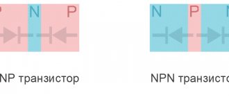
The design circuit of a PNP-type transistor consists of two regions of p-type semiconductor material on either side of a region of n-type material, as shown in the figure below.
The arrow identifies the emitter and the generally accepted direction of its current (“inward” for a PNP transistor).
The PNP transistor has very similar characteristics to its NPN bipolar counterpart, except that the directions of currents and voltage polarities in it are reversed for any of the possible three connection schemes: common base, common emitter and common collector.
PNP transistor designation
PNP transistor symbol Where, E = emitter, B = base, C = collector
The middle level (N-type) is called the B-Base terminal. The left side P-type layer acts as the E-Emitter pin and the right side P-type layer known as the C-Collector pin. PNP transistor
When forming an NPN transistor, one P-type semiconductor material is placed between two N-type semiconductors, as described in the article (Link NPN Transistor). While in a PNP transistor, one N-type semiconductor is placed between two P-type semiconductor materials.
The PNP transistor uses two types of diodes. These are PN and NP diodes, respectively. These PN junction diodes are called collector-base junction or CB junction and base-emitter junction or BE junction.
In a P-type semiconductor material, the charge carriers are primarily holes. Thus, in this transistor, current generation occurs only due to the movement of the holes.
The emitter and collector (P-type) regions are comparatively more doped than the N-type base. The Emitter and Collector regions are wider compared to the base.
Typically, an N-type semiconductor has more free electrons available. But the width of the middle layer in this case is narrower and slightly alloyed. Connecting a transistor, image credit – S. Blank, PNP transistor, CC BY-SA 4.0
Why do you need a transistor?
I often have a question: why do we need a transistor? Why not connect the LED and resistor directly to the battery?
The advantage of a transistor is that you can use a small current or voltage to control a much larger current and voltage.
This is very useful if you want to control things like motors, high power LEDs, speakers, relays and more using a microcontroller/Raspberry Pi/Arduino. The output of the microcontroller can only provide a few milliamps at 5V. So if you want to control, for example, a 230V street light, you cannot do it directly with the microcontroller
You can use a relay instead. But even a relay usually requires more current than the microcontroller output can provide. Therefore you will need a transistor to drive the relay:
It will be interesting➡ Magnetic starters. How does a magnetic starter work?
Transistor light bulb regulator
Well, now it's a matter of practice. Let's assemble the circuit in real life:
I twist the variable resistor and make sure that the light bulb burns at full intensity:
I turn it a little more and the light bulb shines to the floor:
I unscrew the variable resistor all the way and the light goes out:
Instead of a light bulb, you can take any other load, for example, a fan from a computer. In this case, by changing the value of the variable resistor, I can control the fan speed, thereby decreasing or increasing the air flow.
Here the fan does not spin, since I set a high resistance on the variable resistor:
Well, here, by turning the variable resistor, I can already adjust the fan speed:
We can say that the result is a ready-made scheme for blowing yourself on a hot summer day ;-). It became cold - I reduced the speed, it became too hot - I increased it 
Experienced electronics geeks may say: “Why did everything have to be so complicated? Wouldn't it be easier to just take a variable resistor and connect it in series with the load?
Yes, you can.
But some conditions must be met. Let's assume we have a high-power incandescent lamp, which means the current in the circuit will also be decent. In this case, the variable resistor must be of high power, since when twisted all the way towards the small resistance, a large current will flow through it. Let's remember the formula for the power allocated to the load: P=I2R. The variable resistor will burn out (tested more than once from my own experience).
In a circuit with a transistor, the transistor takes on all the responsibility, that is, all the power dissipation. In a circuit with a transistor, it will no longer be possible to burn out a variable resistor, since the current in the base circuit is tens or even hundreds of times less (depending on the beta of the transistor) than the current through the load, in our case through the light bulb.
The transistor will heat up to its maximum only when we regulate the load power by half. In this case, half of the cut-off power in the load will be dissipated by the transistor. Therefore, if you are regulating a powerful load, then first take an interest in such a parameter as the power dissipation of the transistor and, if necessary, do not forget to place transistors on radiators.
The main differences between the two types of bipolar transistors
The main difference between them is that holes are the main current carriers for PNP transistors, NPN transistors have electrons in this capacity. Therefore, the polarities of the voltages supplying the transistor are reversed, and its input current flows from the base. In contrast, with an NPN transistor, the base current flows into it, as shown below in the circuit diagram for connecting both types of devices with a common base and a common emitter.
The operating principle of a PNP-type transistor is based on the use of a small (like the NPN-type) base current and a negative (unlike the NPN-type) base bias voltage to control a much larger emitter-collector current. In other words, for a PNP transistor, the emitter is more positive with respect to the base and also with respect to the collector.
The principle of operation of a bipolar transistor
Now we will try to figure out how a transistor works. I will not go into details of the internal structure of transistors as this information will only confuse. Better take a look at this drawing.
This image best explains the working principle of a transistor. In this image, a person controls the collector current using a rheostat. He looks at the base current; if the base current increases, then the person also increases the collector current, taking into account the gain of the transistor h21E. If the base current drops, then the collector current will also decrease - the person will correct it using a rheostat.
This analogy has nothing to do with the actual operation of a transistor, but it makes it easier to understand the principles of its operation.
For transistors, rules can be noted to help make things easier to understand. (These rules are taken from the book “The Art of Circuit Design” by P. Horowitz W. Hill).
- The collector has a more positive potential than the emitter
- As I already said, the base-collector and base-emitter circuits work like diodes
- Each transistor is characterized by limiting values such as collector current, base current and collector-emitter voltage.
- If rules 1-3 are followed, then the collector current Ik is directly proportional to the base current Ib. This relationship can be written as a formula.
From this formula we can express the main property of a transistor - a small base current controls a large collector current.
- current gain.
It is also denoted as
Based on the above, the transistor can operate in four modes:
- Transistor cutoff mode - in this mode, the base-emitter junction is closed, this can happen when the base-emitter voltage is insufficient. As a result, there is no base current and therefore there will be no collector current either.
- The active mode of a transistor is the normal mode of operation of the transistor. In this mode, the base-emitter voltage is sufficient to cause the base-emitter junction to open. The base current is sufficient and the collector current is also available. The collector current is equal to the base current multiplied by the gain.
- Transistor saturation mode - the transistor enters this mode when the base current becomes so large that the power of the power source is simply not enough to further increase the collector current. In this mode, the collector current cannot increase following an increase in the base current.
- Inverse transistor mode - this mode is used extremely rarely. In this mode, the collector and emitter of the transistor are swapped. As a result of such manipulations, the gain of the transistor suffers greatly. The transistor was not originally designed to operate in such a special mode.
To understand how a transistor works, you need to look at specific circuit examples, so let's look at some of them.
Let's consider a circuit with a different load
Figure 2. Controlling a powerful load
We need to turn on the motor with an operating current of 0.7 A. To turn it on, we need a more powerful transistor. Let's take the SS8050 transistor with a maximum allowable collector current of 1.5 A. This transistor has a minimum current transfer ratio of 120. With a collector current of 0.7 A, we need to provide a minimum base current of 5.8 mA. Taking into account the fact that it is necessary to implement a saturation coefficient greater than one, we are left with a working option for a base current of 10 mA. At a given collector current of 0.7 A, the base saturation voltage of this transistor will be about 1.2 V (according to the documentation for the transistor). The voltage across the base resistor is 2.1 V. The minimum resistance of the base resistor is 2.1 V / 0.010 A = 210 Ohms. The maximum resistance of the base resistor is 2.1 V / 0.0058 A = 360 Ohms. If we supply a base resistor greater than 360 Ohms, the transistor will obviously not open completely and will not provide an output current of 0.7 A.
With a collector current of 0.7 A, the collector saturation voltage will be about 0.2 V. The power dissipated at the transistor collector will be about 0.14 W, and the transistor will be noticeably warm.
Additionally, I note that the DC electric motor is an inductive load and it is necessary to install a protective diode in parallel with it, which will protect the transistor from self-induction EMF when the transistor is turned off. The rated current of this diode must be equal to or greater than the operating current of the inductive load. The operating voltage of the diode must be greater than the load supply voltage.
An important point needs to be made. The greater the base current, the faster the transistor turns on, the greater the saturation coefficient. The higher the saturation coefficient, the slower the transistor will turn off. The shutdown delay can reach several hundred nanoseconds. At first glance, this value seems too small to pay attention to. In fact, if you control the current through the load using PWM, or try to increase the data transfer rate through the infrared channel, you will find that the turn-off delay of the transistor will greatly distort the signal.
For example, let's take a PWM frequency of 20 kHz with a resolution of 8 bits. The PWM period will be 50 microseconds, the resolution of one step will be about 200 nanoseconds. Delaying the turn-off of the transistor by 400 nanoseconds will absorb the resolution of the two least significant bits and leave only 6 bits of dynamic range from the 8-bit resolution.
To increase the turn-off speed of the transistor, there are methods that we will consider later.
NPN transistor operation:
Now that the n side of the diode has the most electrons and the p side has the most holes, all voltage connections are arranged as forward and reverse bias respectively. The emitter base junction is configured as reverse bias and the collector base junction is configured as forward bias. The depletion region of this emitter-base region is narrower compared to the depletion region at the collector-base intersection.
Since the junction is reverse biased (emitter), the holes flow from the power supply to the N junction. The electron then moves towards p. Here some electron is neutralized. The remaining electrons move towards n. The voltage drop relative to the emitter and base is VBE as the input side.
In N-type emitters, the charge carriers are mainly electrons. Consequently, electrons are transferred through the N-type emitters to the P-type base. The current will flow through the emitter-base or EB junction. This current is known as emitter current (Ie). Here, the emitter current (IE) flows from the output side and flows in two directions; one is IB and the other is IC. So we can write:
It will be interesting➡ How to connect an LED strip? Simple ways to connect LED strip
IE=IB+IC
However, the base region is relatively thin and lightly doped. Consequently, most of the electrons pass through the base region and only a few of them recombine with the available holes. The base current is minimal compared to the emitter current. Typically this is up to 5% of the total emitter current.
The current flowing from the rest of the electrons is called collector current (IC). YC is relatively high compared to baseline (IB).
Advantages of the Darlington circuit
Darlington transistors are used in the same way as single bipolar ones. They can be considered as one transistor with changed parameters. The most important feature of this change is the multiplication of the current gains.
Let's return to the example given at the beginning: combining a power transistor with β = 40 with a smaller value of β, we get a gain of 1600. To turn on a load that consumes 5 A, only 3 mA is required - this is the current that most microcontrollers successfully provide.
Read also: What is a smartphone?
However, it must be remembered that the transistors in this connection are not evenly loaded: most of the current passes through T2. This means that they do not have to be the same type. For example, T1 could be a low power transistor with a large β, making the resulting gain even higher!
Transistor operating mode
It has three operating modes according to the offset, namely:
- Active mode
- Shutdown mode
- Saturation mode
Shutdown mode
- The transistor operates as an open circuit.
- At cutoff, the two junctions are reverse biased.
- No current will be allowed to flow.
Saturated mode
- The transistor is made in a closed circuit.
- Both transitions are configured for forward bias only.
- Since the base-emitter voltage is relatively high, current flows from the collector to the emitter.
Active mode
- At this time, the transistor operates as a current amplifier circuit.
- In the active mode of the transistor, the BE junction is forward biased and the C -B junction is reverse biased.
- Current flows between the emitter and collector, and the magnitude of the current is proportional to the applied base available.
Darlington circuit in practice
It's time to test the properties of the Darlington circuit in practice. Of course, according to the previous diagram, such a configuration can be built “manually” using two transistors. However, this circuit is so popular that manufacturers also sell ready-made Darlington transistors that have this dual connection and look like a regular single transistor.
In our experiment, we will use the MPSA29 (β>10000) transistor , which is an off-the-shelf Darlington transistor. Let's compare its performance with the previously reviewed BC546 (β = 200–450). This time, we'll build two versions of a "graphite paper potentiometer" in which one of the paths through which current flows will be drawn in pencil on a piece of paper!
Read also: What is soldering?
To complete this exercise you will need:
- Resistor 1 × 10 kOhm,
- Resistor 1 × 1 kOhm,
- 1 × LED (choose your favorite color),
- 1 × BC546 transistor,
- 1 × MPSA29 transistor,
- 1 × pencil,
- 1 × sheet of paper,
- 4 × AA batteries, 1 × slot for 4 AA batteries,
- 1 × development board,
- set of connecting wires.
| When doing the exercises, note that the BC546 and MPSA29 transistors have different pin positions (see below for details)! |
First make the potentiometer by yourself. On a piece of paper, draw a thick line with a pencil, several centimeters long. Draw the pencil along the line several times to make sure it is clear (one stroke is not enough because the carbon footprint on the sheet will not be continuous). As you probably know, graphite conducts electricity, but has a fairly high resistance. By drawing a line, you have made a resistor with a resistance of hundreds of kilo-ohms per centimeter. You can check this with help. multimeter.
Using a multimeter, you can measure the resistance of a line drawn with a pencil
Now we need to place a chip on the breadboard that will use our graphite resistor . For now we will use the well known BC546 transistor. However, you should immediately pay attention to the different pinout arrangement of the MPSA29!
Comparison of BC546 and MPSA29 transistor pinouts
We will use the graphite line as a "potentiometer" to regulate the current flowing through the base. Simply press the wires onto a piece of paper. The greater the distance between the conductors, the greater the resistance between them. A 10 kOhm resistor is used to protect the transistor from fire if these wires are accidentally short-circuited.
Circuit diagram for BC546 gain testing
In practice, the whole scheme might look like this:
| Assembling the circuit on a breadboard | Scheme with BC546 in practice |
It's time to check how the circuit behaves at different resistances . When performing this exercise, do not touch the “potentiometer” wires with your fingers - the skin resistance is relatively low, which will disrupt the progress of this experiment.
| Resistance is low - LED is on | Resistance is high - LED does not light up |
The longer the path between the ends of the wires, the higher the resistance and less current flows into the base. At what length of the track does the LED stop lighting? Record your result, turn off the power and replace the transistor with an MPSA29. However, remember that this transistor has a different emitter and collector!
Circuit diagram for MPSA29 amplification testing
In practice, the whole scheme might look like this:
| Circuit on breadboard | Example with MPSA29 |
After assembling the circuit, turn on the power, and again press the ends of the wires to the track on the sheet. Now the distance between the wires on which the LED lights up should be much greater. This is all thanks to the properties of the new transistor, which has a much higher beta gain.
| Resistance is low - LED is on | Resistance is high - LED is still on |
Checking a bipolar transistor with a multimeter
This is the most common component, for example the KT315, KT361 series, etc.
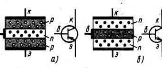
There will be no problems with testing this type; it is enough to imagine the pn junction as a diode. Then the pnp and npn structures will look like two counter- or reverse-connected diodes with a midpoint (see Fig. 3).
“Diode analogues” of pnp and npn junctions
We connect the probes to the multimeter, the black one to “COM” (this will be a minus), and the red one to the “VΩmA” socket (plus). We turn on the testing device, switch it to the dialing or resistance measurement mode (it is enough to set the limit to 2 kOhm), and begin testing. Let's start with pnp conductivity:
- We attach the black probe to terminal “B”, and the red one (from the “VΩmA” socket) to leg “E”. We look at the multimeter readings; it should display the value of the junction resistance. The normal range is 0.6 kOhm to 1.3 kOhm.
- In the same way we take measurements between terminals “B” and “K”. The readings should be in the same range.
If during the first and/or second measurement the multimeter displays minimum resistance, then there is a breakdown in the transition(s) and the part requires replacement.
- We reverse the polarity (red and black probe) and repeat the measurements. If the electronic component is working properly, the resistance will be displayed, tending to the minimum value. If the reading is “1” (the measured value exceeds the capabilities of the device), an internal break in the circuit can be stated, therefore, the radio element will need to be replaced.
Testing a reverse conduction device follows the same principle, with a slight modification:
- We connect the red probe to leg “B” and check the resistance with the black probe (touching terminals “K” and “E” in turn), it should be minimal.
- We change the polarity and repeat the measurements, the multimeter will show a resistance in the range of 0.6-1.3 kOhm.
Deviations from these values indicate a component failure.
Step-by-step instructions for checking with a multimeter
Before starting the test, first of all, the structure of the triode device is determined, which is indicated by the emitter junction arrow. When the direction of the arrow points towards the base, then this is the PNP variant, the direction opposite to the base indicates NPN conductivity.
Testing a PNP transistor with a multimeter consists of the following sequential operations:
- We check the reverse resistance; to do this, we connect the “positive” probe of the device to its base.
- The emitter junction is tested; for this we connect the “negative” probe to the emitter.
- To check the collector, move the negative probe onto it.
The results of these measurements should show a resistance within the value of “1”.
To check direct resistance, swap the probes:
- We attach the “negative” probe of the device to the base.
- We alternately move the “positive” probe from the emitter to the collector.
- On the multimeter screen, the resistance readings should be from 500 to 1200 Ohms.
These readings indicate that the transitions are not broken, the transistor is technically sound.
Many amateurs have difficulty identifying the base, and, accordingly, the collector or emitter. Some advise starting to determine the base, regardless of the type of structure, in this way: alternately connecting the black probe of the multimeter to the first electrode, and the red probe alternately to the second and third.
The base will be detected when the voltage across the device begins to drop. This means that one of the transistor pairs has been found - “base-emitter” or “base-collector”. Next, you need to determine the location of the second pair in the same way. The common electrode of these pairs will be the base.
It will be interesting➡ Total resistance
Verification methods
Any repair of electronics and electrical equipment begins with an external inspection, and then proceeds to measurements. This approach allows you to localize most faults. To find a varistor on the board, look at the figure below - this is what varistors look like. Sometimes they can be confused with capacitors, but can be distinguished by their markings.
If the element is burnt out and the markings cannot be read, look at this information on the device diagram. On the board and in the diagram it can be designated by the letters RU. The conventional graphic symbol looks like this.
There are three ways to test a varistor quickly and easily:
- Visual inspection.
- Call. This can be done with a multimeter or any other device that has a continuity test function.
- Resistance measurement. This can be done with a high-range ohmmeter, multimeter or megger.
A varistor fails when a large or prolonged current passes through it. Then the energy is dissipated in the form of heat, and if its amount is greater than that determined by the design, the element burns out. The housing of these components is made of a hard dielectric material, such as ceramic or epoxy coating. Therefore, when it fails, the integrity of the outer coating is most often damaged.
You can visually check the varistor for functionality - there should be no cracks on it, as in the photo:
The next method is to check the varistor with a tester in continuity mode. This cannot be done in the circuit, because the dialing can work through parallel-connected elements. Therefore, you need to unsolder at least one of its legs from the board.
Important: you should not check the elements for serviceability without desoldering them from the board - this may give false readings from the measuring instruments. Since in the normal state (without voltage applied to the terminals) the resistance of the varistor is high, it should not ring through. The test is performed in both directions, that is, by swapping the multimeter probes twice
The test is performed in both directions, that is, by swapping the multimeter probes twice
Since in the normal state (without voltage applied to the terminals) the resistance of the varistor is high, it should not ring through. The test is performed in both directions, that is, by swapping the multimeter probes twice.
On most multimeters, the continuity mode is combined with the diode testing mode. It can be found by the diode icon on the mode selector scale. If there is a sound indication sign next to it, it probably also has a dial tone.
Another way to test a varistor for breakdown with a multimeter is to measure the resistance. You need to set the device to the maximum measurement limit, in most devices this is 2 MOhms (megaohms, designated as 2M or 2000K). The resistance must be equal to infinity. In practice, it can be lower, within 1-2 MOhm.
Interesting! The same can be done with a megaohmmeter, but not everyone has one. It is worth noting that the voltage at the megohmmeter terminals should not exceed the classification voltage of the component being tested.
This ends the available methods for checking a varistor. This time, the multimeter will help the radio amateur find the faulty element, as in a large number of other cases. Although in practice a multimeter is not always needed in this matter, because the matter rarely goes beyond a visual inspection. Replace the burnt element with a new one, designed for voltage and with a diameter no less than the burnt one, otherwise it will burn out even faster than the previous one.
Adviсe
- There are many ways to determine a malfunction, but first you need to understand the structure of the element itself and clearly understand the design features.
- The choice of device for testing is an important point regarding the quality of the result. Therefore, if you lack experience, you should not limit yourself to improvised means.
- When carrying out the test, you should clearly understand the reasons for the failure of the tested part, so as not to return over time to the same state of failure of household electrical appliances.
Applications of PNP transistors:
- PNP transistors are used as switches i.e. analog switches, emergency buttons, etc. They are used when emergency shutdown is required.
- These types of transistors are used in current source circuits, i.e., by taking advantage of the characteristics of the current flowing from the collector.
- Used in amplification circuits.
- They are used in paired Darlington circuits.
- PNP transistors are used in heavy-duty motors for current control and in various robot and microcontroller development applications.
Next
MiscellaneousWhat is active power?
Advantages and disadvantages of composite transistors
The power and complexity of a Darlington transistor can be adjusted by increasing the number of bipolar transistors included in it. There is also an IGBT transistor, which includes a bipolar transistor and a field effect transistor, used in the field of high voltage electronics.
The main advantage of composite transistors is their ability to provide high current gain. The fact is that if the gain of each of the two transistors is 60, then when they work together in a composite transistor, the total gain will be equal to the product of the coefficients of the transistors included in its composition (in this case, 3600). As a result, a fairly small base current is required to open the Darlington transistor.
The disadvantage of composite transistors is their low operating speed, which makes them suitable for use only in circuits operating at low frequencies. Often, composite transistors appear as a component of the output stages of powerful low-frequency amplifiers.
Next
MiscellaneousWhat is active power?