Definition
Torsion device model
Slopeness is often denoted as conductivity, g
m, with subscript m for
mutual
.
This is defined as follows: g m = Δ I out Δ V in { displaystyle g_{m} = { frac { Delta I_{ text {out))} { Delta V_{ text {in))))}
For a weak signal alternating current, simpler definition:
g m = i out v in { displaystyle g_{m} = { frac {i_{ text{out))} {v_{ text{in))))}
To the block, Siemens
, with symbol,
S
;
1 Siemens = 1 ampere per volt replaced the old unit of conductivity, which had the same definition, Mxo
(ohm spelled backwards), symbol,
℧
.
Bipolar transistors
| Item: | Physics |
| Kind of work: | Course work |
| Language: | Russian |
| Date added: | 11.02.2019 |
- This type of work is not a scientific work, it is not a finished final qualifying work!
- This type of work is a finished result of processing, structuring and formatting collected information intended for use as a source of material for independent preparation of educational work.
If you have a hard time understanding this topic, write to me on WhatsApp, we’ll look into your topic, agree on a deadline, and I’ll help you!
At this link you can find many ready-made coursework in physics:
| A lot of ready-made coursework in physics |
Check out these similar threads, they might be useful to you:
| Asynchronous motor |
| Non-contact temperature control methods |
| Boris Semenovich Jacobi - physicist and inventor |
| The greatest discoveries of physics |
Introduction:
For most of the 20th century, physics was a mainstream science. Electrification, cars, space flights, the atomic bomb - humanity owes all these achievements to physics.
Electronics, which is based on physical processes, that is, real physics, has already changed the world to a significant extent. The current stage of development of human society is characterized by the increasing penetration of electronics into all spheres of human life and activity. Advances in this area greatly contribute to solving complex scientific and technical problems, increasing the efficiency of scientific research, creating new types of machines and equipment, developing effective technologies and control systems, obtaining materials with unique properties, improving the collection and processing of information, and more.
The last information direction is currently the most relevant and well-known. It is absolutely impossible to imagine our world without personal computers, laptops, smartphones, tablets - everything without which information technology is unthinkable. However, all this has become our reality only and exclusively thanks to the development of microelectronics.
The first machines that can be described using the term "computer" appeared in the 1940s. The computer was based on vacuum tubes with a diameter of about 12 mm and a height of 40 mm. They were replaced by transistors, which later gave way to integrated silicon circuits.
Soon after the birth of microelectronics, it became clear that its development would be rapid. As the number of transistors increases, the power of the corresponding computing devices increases.
For a long time this rule, called Moore's law, was followed, but recently the growth rate of the number of transistors has begun to fall. The reason for this was the approach to the physical limit - the size of transistors was reduced to tens of nanometers.
Bipolar Transistor Gain Property
General information about transistors
Transistors are semiconductor devices that have at least three wires and, under certain circumstances, can amplify power, convert a signal, or generate oscillations. There are many different types of transistors - these are field-effect (unipolar) and bipolar transistors, insulated gate bipolar transistors and unijunction (double base) transistors, phototransistors and others.
Amplifier stages made with transistors require a low supply voltage, only a few volts, and the efficiency can reach several tens of percent. Compared with vacuum tubes, transistors have higher efficiency, low power consumption, long MTBF, light weight and size, and high mechanical strength. The disadvantages of transistors include low radiation resistance, the inability to operate at temperatures of the semiconductor silicon crystal significantly exceeding 125 ° C, etc.
Transistors are classified according to semiconductor materials, dividing them into germanium, silicon, gallium arsenide and others.
Bipolar transistors in which two of the three regions have hole-type conductivity are called forward conduction transistors or pnp structures. And bipolar transistors, in which two of the three regions have an electronic type of conductivity, are called reverse conduction transistors or npn structures.
The devices in question, which are not capable of amplifying a signal with a frequency of more than 3 MHz, are called low-frequency transistors. Devices that can amplify signals with frequencies greater than 3 MHz but less than 30 MHz are called mid-range transistors. And transistors that allow signal amplification with a frequency exceeding 30 MHz are called high-frequency, and transistors that allow operation at an even higher frequency (above 300 MHz) are called ultra-high-frequency.
If the components cannot provide power dissipation greater than 0.3 W, then such transistors are called low power transistors. Devices with power dissipation greater than 0.3 W but less than 3 W are called mid-power transistors. And transistors whose power dissipation exceeds 3 W are called high-power transistors.
Bipolar transistors
Bipolar transistor, developed in 1949-1950. American physicist W. Shockley is the most common type of amplifying semiconductor device and is a universal element of electronic technology.
Here are the most important characteristics of a typical low-power silicon transistor: the forward transfer characteristic and the family of output characteristics—at a given emitter current and at a given base emitter voltage. Let's note the main thing.
For those values of collector current Ik that are acceptable for a particular device, the voltage between the base and emitter of the transistor should almost always be in the range of 0.6-0.7 V.
The transconductance of the forward transmission of a bipolar transistor is very high (tens and hundreds of mA/V).
The output resistance of the transistor at a given emitter current is very high - at least 1 MOhm.
The amplifying properties of the transistor are maintained when the voltage between the collector and base Ikb drops to zero.
The collector and emitter currents are almost equal to each other. More precisely, they differ from each other in the small amount of base current.
Moreover, the ratio of the transistor is a parameter - the current transfer coefficient, denoted by h21E (a variant can also be found).
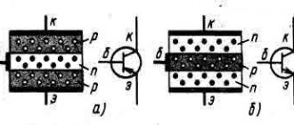
Bipolar transistors are semiconductor devices with two interacting electrical pn junctions that are capable of amplifying a power signal from an external power source. The simplest transistor is a semiconductor Troid with two pn junctions.
In a bipolar transistor, two types of charges, electrons and holes, simultaneously participate in the transmission of current. Transistor junctions are formed by three regions with alternating types of conductivity. Depending on the order of alternation of these areas, transistors of the npn and pnp types are distinguished. NPN type transistors are preferred because the mobility of electrons in them is higher than the mobility of holes.
The connection operating in the forward direction is called the emitter, and the corresponding outer layer is called the emitter. The middle layer is called the base layer. The base has the opposite type of conductivity and always has a high resistance, i.e. the concentration of holes in it is many times lower than the concentration of electrons in the emitter.
The second junction, usually biased in the opposite direction, is called the manifold, and the outermost layer is called the manifold. This name reflects the function of collecting injected carriers that have passed through the base layer. The electron concentration in it is also high, it is only slightly lower than in the emitter.
A transistor is, generally speaking, a reversible device, meaning the emitter and collector can be changed to keep the device operating. However, due to the asymmetry of the actual structure, as well as the difference in emitter and collector materials, the normal and reverse connections of the transistor are not the same.
Depending on the transistor manufacturing technology, the concentration of impurities in the base can be distributed evenly or unevenly. With a uniform distribution, there is no internal field, and minority carriers at the base move through it due to the diffusion process. Such transistors are called diffusion or drift.
When the impurity concentration is unevenly distributed in the base, an internal electric field arises, and minority charge carriers move in it as a result of drift and diffusion, with drift playing a dominant role.
Operating principle of bipolar transistors
If a voltage is applied to the transistor at the emitter junction in the forward direction and at the collector junction in the opposite direction, and Ek >> Ee (Ek = 110 V, Ee = 0.11 V), then the emitter junction opens, its potential barrier decreases, the junction narrows , its resistance decreases, and the process of injection of charge carriers from the emitter into the base (in our case, electrons) begins, since the concentration of electrons in the emitter is much higher than the concentration of holes in the base. Consequently, the base is filled with minority charge carriers, and since the base thickness w in real transistors is made smaller than the electron mean free path L, only a small fraction of the electrons injected into the base recombine with the base holes. The charge of the recombined electrons remains in the base and additional positive charge must come from the external circuit to restore the electrical neutrality of the base, so the base current is the recombination current.
Most of the electrons injected into the base do not have time to recombine with holes and fall near the collector field in an electric field that is accelerated for them because the collector junction is turned on in the opposite direction and the electrons in the bases are minority shareholders. Therefore, all the electrons from the base enter the collector, forming a collector current in the external circuit. In addition to the current caused by minority charge carriers injected into the base, a normal reverse runaway current ko flows through the pn junction collector, biased in the opposite direction. Thus, the total current in the circuit will be e = k + b + k.
Since the base has high resistance, it can be assumed that holes do not pass into the emitter because they recombine with electrons in the base. Recombination produces a base current that is small because the hole concentration at the base is low.
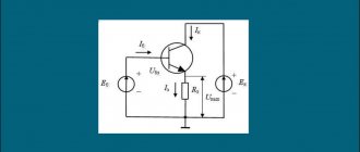
In this circuit, the transistor is connected with a common base in which the emitter current is the input current e = in and the collector current is the output to = out. For a transistor, it is important to know the relationship between input and output current, therefore, to calculate equivalent electrical circuits, the following parameter is introduced - the current transfer coefficient.
Electron injection coefficient, showing what part of the total emitter current is its electronic component, since the hole component, which is much smaller than the first, is also included in the total emitter current; k is the coefficient of electron transfer through the base, which shows the fraction of injected electrons reaching the collector and depends on the thickness of the base, which, in turn, depends on the voltage at the pn junction.
Let us now assume that an alternating signal Uin is received at the input of this circuit. In this case, the emitter input current in = e = Uin / Re will begin to flow through the open contact of the emitter. The collector current is approximately equal to the emitter current, then at the output of the transistor, at the collector connection, an alternating signal will appear equal to Uout = Uk = k * Rk. Transistor voltage gain:
Since the closed collector junction resistance is much greater than the open emitter junction, the transistor voltage gain for this circuit will be very large. Thus, the common base transistor switching circuit does not amplify the current signal, but does a very good job of amplifying the voltage signal. Amplification occurs due to an external power source.
Bipolar transistor switching circuits
The signal source is connected between the base and emitter of the transistor connected in a common emitter circuit, and the load is connected to the collector. Poles of the same power supply signs are connected to the emitter of the transistor. The input current of the stage is the base current of the transistor, and the output current is the collector current.
In practice, they are driven by one power supply rather than two. Turning on an NPN transistor is exactly the same as turning on a PNP transistor, but in this case you have to change the polarity of both the power supplies.
The gain of the cascade is equal to the ratio of the collector current to the base current and can usually range from tens to several hundreds. A transistor connected in accordance with the common emitter circuit can theoretically give the maximum signal gain compared to other transistor connection options. The input impedance of the stage in question, equal to the ratio of the base emitter voltage to the base current, lies in the range from hundreds to thousands of ohms. This is less than a cascade with a transistor connected to a common collector circuit. The common emitter output stage has a phase shift of 180° from the input. Temperature fluctuations have a significant impact on the operating mode of the transistor connected to the common emitter circuit, and therefore special temperature stabilization circuits should be used. Due to the fact that the collector junction resistance of the transistor in the cascade under consideration is higher than in the common-base cascade, it takes more time for charge carriers to recombine, and, therefore, the common-emitter cascade has a worse frequency property.
The load is connected to the emitter of the transistor, connected in a circuit with a common collector, the input signal is supplied to the base. The input current of the stage is the base current of the transistor, and the output current is the emitter current.
The output signal is taken from a load resistor connected in series with the emitter terminal. The input of the stage has high resistance, usually from tenths of a megohm to several megohms, due to the fact that the transistor's collector connection is blocked. The output impedance of the stage, on the contrary, is low, which makes it possible to use such stages to match the previous stage with the load. A stage with a transistor connected according to a common collector circuit does not amplify the voltage, but amplify the current (usually 10 ... 100 times). The phase of the input voltage of the signal supplied to the cascade coincides with the phase of the output voltage, that is, there is no inversion. It is because of the preservation of the phase of the input and output signals that the common collector stage has another name - emitter follower. The temperature and frequency properties of the emitter follower are worse than those of a stage in which the transistor is connected in accordance with a common base circuit.
In a cascade assembled according to a common basic circuit, the voltage at the input signal is applied between the emitter and the base of the transistor, and the output voltage is removed from the terminals at the collector base.
In this case, the emitter connection of the component is open and its electrical conductivity is high. The input resistance of the stage is small and usually ranges from a few to hundreds of ohms, which is explained by the disadvantage of the described inclusion of the transistor. In addition, to operate a stage with a transistor connected in a common-base circuit, two separate power supplies are required, and the stage current gain is less than unity. The stage voltage amplification often ranges from tens to several hundred times.
Advantages include the ability to operate the cascade at a significantly higher frequency compared to the other two transistor switching options and the weak influence of temperature fluctuations on the operation of the cascade. This is why stages with transistors connected in a common basic circuit are often used to amplify high-frequency signals.
Types of bipolar transistors
The point-point transistor is the first semiconductor device in which the amplification effect was discovered. This is a phenomenon in which the probe current follows the change in current of the main contact with a significant reverse voltage. When forming contacts under the needles, layers are formed: p-type under the emitter, double pn-layer under the collector. The main difference is that in these structures there is an increase in the current in the circuit with OF, i.e. B> 1. The permissible power dissipation of such devices is small and amounts to several 100 mW, Iko? 1h2 mA, rc = 7h15 kOhm, re? rb = up to 500 Ohm, that is, their parameters are much worse than those of planar ones. And today they have been successfully replaced by drift and avalanche transistors.
An avalanche transistor is a device that uses impact ionization in the collector junction, which allows one to obtain an S-shaped (ambiguous in voltage) output characteristic in a circuit with an OE. Simplified formula for resistance: rk = UM (-db / dIe) / .
Thus, the characteristics of an avalanche transistor resemble those of a thyristor or thyratron. It is interesting to note that in the case of Ib > 0 a “negative cross-section” is also possible in principle, but this requires a very critical combination of parameters.
The main disadvantage of such a device is the high voltage on the collector.
A unijunction transistor (UJT) is a device with “negative” resistance, in which the load current can increase even as Uin decreases. If OPT is enabled, it can only be disabled by opening the circuit or removing Uin. OPT implements various starting voltage sources. You can apply Ucm
· Statistical induction transistor (SIT) is a pn junction field effect transistor that can operate in either reverse bias (FET mode) or forward bias (BT gate). Unlike BT, the reverse voltage applied to the gate of the transistor can reach 30 V, which greatly accelerates the resorption process of minority carriers that appear in the forward biased gate channel. SIT, like IGBT, has a large gate capacitance, the recharging of which requires significant control currents. The advantage of SIT over BT is its increased productivity. The turn-on time is practically independent of the operating mode, the turn-off time depends on the ratio of the drain and gate currents. A feature of the SIT that makes it difficult to use as a switch is its normally open state in the absence of control current. The advantages of SIT also include low channel resistance in the open state, which is 0.1 - 0.025 Ohm.
Insulated Gate Bipolar Transistors (IGBTs)
We will look at them in more detail.
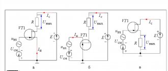
IGBTs are made as a combination of an input unipolar (field-effect) isolated gate transistor (IGBT) and an output bipolar npn BT. There are many different ways to create such devices, but the most common are IGBT (insulated gate bipolar transistor) devices, which successfully combine the properties of FETs with a vertical channel and an additional bipolar transistor. Thus, the IGBT has three external leads: emitter, collector, gate. The emitter and drain (D) and base and source (S) connections are internal. The combination of two devices in one structure allowed us to combine the advantages of field-effect and bipolar transistors: high input impedance with high current load and low resistance.
IGBT structure
In the diagram, VT represents the insulated gate FET, VT1 represents the bipolar transistor, R1 represents the series resistance of the FET channel, R2 represents the resistance that bypasses the base-emitter junction of the bipolar transistor VT1. Due to resistance R2, the bipolar transistor is blocked and does not significantly affect the operation of the field-effect transistor VT. The structure of the IGBT transistor is complemented by another pn junction, thanks to which another pnp transistor VT2 appears in the equivalent circuit. The resulting structure of the two transistors VT1 and VT2 has deep internal positive feedback, since the collector current of transistor VT2 affects the base current of transistor VT1, and the collector current of VT1 determines the base current of transistor VT2.
Assuming that the emitter current transfer coefficients of transistors VT1 and VT2 have values b1 and b2, respectively, we find Ik2 = b2Ie2, Ik1 = b1Ie1 and Ie = Ik1 + Ik2 + Ic. From the last equation we can determine the drain current of the field-effect transistor Ic = Ie (1 - b1 - b2).
Since the drain current Ic PTIZ can be found through the slope S and the gate voltage Uz Ic = SUz, we determine the current of the IGBT transistor: Iк = Iз = SkUz, where Sk = S / [1-] is the equivalent transconductance of the BT with an insulated gate.
Schematic diagram of IGBT. It emphasizes its hybridity in the sense that the insulated gate is depicted as in PTIZ, and the collector and emitter electrodes are depicted as in BT.
Another advantage of IGBT is that the series resistance is greatly reduced and hence the voltage drop across the closed switch is reduced. The latter is explained by the fact that the series resistance of the R2 channel is shunted by two saturated transistors VT1 and VT2 connected in series.
The safe operation zone of the IGBT is similar to that of the IGBT, i.e., it does not have a secondary breakdown area characteristic of bipolar transistors. Since it is based on channel-induced IGBT transistors, the voltage applied to the gate must be greater than the threshold voltage, which is 5-6 V.
The speed of IGBT is slightly lower than the speed of PT, but significantly higher than the speed of BT. Research has shown that for most IGBT transistors, the turn-on and turn-off times do not exceed 0.55 x 1.0 μs.
Microsemi NPT Power IGBT 650V for industrial applications
Microsemi Corporation today announced the availability of a new family of 650V NPT IGBTs in 45A, 70A and 95A operating currents.
The new bipolar transistors can operate under harsh conditions and are designed for use in applications such as solar inverters, welders and switching power supplies. Microsemi NPT IGBT transistors can improve the efficiency of final solutions due to lower losses compared to the closest analogues (by approximately 8%).
New models provide switching frequencies of up to 150 kHz, but this level can be increased by using transistors in combination with the key element of microsemiodes made using silicon carbide technology. All members of the new generation Microsemi 650-V NPT IGBT are manufactured using advanced Power MOS 8 technology. This process reduces overall switching losses and allows the elements to operate at significantly higher switching frequencies than competing solutions.
Isolated flat gate bipolar transistors (IGBTs) can be connected in parallel (they have a positive temperature coefficient Vcesat) to improve the reliability of power devices. The short circuit stability time is also standardized, ensuring reliable operation of the devices in harsh industrial environments.
The influence of frequency on the amplifying properties of bipolar transistors
It is known that the higher the frequency of the signal arriving at the input of the transistor stage, the lower the current gain. The main contribution to the decrease in amplifying properties should be attributed to the barrier capacitance and the delay of alternating collector currents from the emitter for the time required for the diffusion of charge carriers in the base region. In addition, the capacitances between the case and the terminals of the transistor negatively affect the amplifying properties of the device.
The collector connection of the transistor has high resistance. An increase in frequency leads to a decrease in the reactive capacitance of the collector collector, which leads to its significant shunting and deterioration of the amplifying properties of the cascade.
Charge carriers cross the main region and recombine in a short finite time interval, tens of nanoseconds. The higher the frequency, the greater the delay of charge carriers. At constant current, the phase shift between the collector and emitter currents of the transistor is zero, and the total base current is minimal. At high frequency there will be a phase shift between the alternating currents of the collector and emitter of the transistor, which was not at direct current. In this case, the total base current of the transistor at high frequency is much higher than the total base current at low frequency and, moreover, at constant current. Increasing the base current to obtain a given fixed collector current means decreasing the transistor current gain.
To increase the cutoff frequency of the transistor gain, it is necessary to make the base region as thin as possible, increase the speed of minority charge carriers passing through it, reduce the capacitance of the housing and transistor terminals, etc.
The influence of temperature on the operating modes of bipolar transistors
To prevent failure of a germanium transistor, its crystal temperature must be below about 70 ° C, a silicon transistor must be less than 125 ... 150 ° C, and a gallium arsenide transistor must be less than 150 ... 200 ° C. The introduction of alloying additives slightly adjusts the maximum permissible crystal temperature, and some specially designed transistors can withstand higher temperatures. Heating of bipolar transistors causes an increase in the conductivity of the base region and the return collector current. When the transistor case temperature increases from 20°C to 60°C, the reverse collector current can typically increase up to six times. Therefore, temperature fluctuations have a very significant effect on the functioning of the transistor stage, causing significant changes in its operating mode. To prevent temperature fluctuations from leading, for example, to self-generation of a cascade intended for amplification or other harmful consequences, it is necessary to use thermal stabilization circuits for the operating modes of transistors.
Conclusion:
Finally, a word about the future: Researchers expect the miniaturization process to end in 2022. Transistors will reach such sizes that they will no longer obey the laws of classical physics on which the operation of all modern computers is based. Currently, research is being conducted all over the world in the field of creating a new element base for electronics. The most promising is the creation of a transistor based on organic compounds and carbon tubes. And if certain encouraging results have already been obtained in the creation of individual transistors, then the prospects for creating microcircuits based on the new element base look more vague. Therefore, the operating principles of traditional semiconductor devices will be in demand for quite some time.
Trans resistance
Trans resistance
(for
transmission impedance
), also rarely called
mutual impedance
, is double transconductance.
It refers to the relationship between the change in voltage at two output points and the corresponding change in current at two input points and is denoted by r m: r m = Δ V out Δ i in { displaystyle r_{m} = { frac { Delta V_{ text { out }}} { Delta I _ { text {in}}}}}
The SI unit of resistance is simply , as in resistance.
Transimpedance
(or,
translation resistance
) is the AC equivalent of resistance and is double transmittance.
Where are field effect transistors used?
The current level of technology makes it possible to make the open channel resistance of a powerful field-effect transistor (FET) quite small - a few hundredths or thousandths of an Ohm!
And this is a great advantage, since when a current of even tens of amperes flows, the power dissipated by the PT will not exceed tenths or hundredths of a watt.
Thus, you can eliminate bulky radiators or greatly reduce their size.
PTs are widely used in computer power supplies and low-voltage switching regulators on the computer motherboard.
Of the variety of types of FETs, FETs with an induced channel are used for these purposes.
Devices
Vacuum tubes
For vacuum tubes, transconductance is defined as the change in plate (anode) current divided by the corresponding change in grid/cathode voltage, with a constant voltage between the plate (anode) and cathode. Typical gm values for a small signal vacuum tube are from 1 to 10 millisiemens. This is one of the three characteristic constants of a vacuum tube, the other two being its gain μ (mu) and the plate resistance rп or rа. The van der Bijl equation defines their relationship as follows:
g m = μ r p { displaystyle g_{m} = { frac { mu} {r_{p)))} [1]
Field effect transistors
Likewise in FETs, and MOSFETs in particular, transconductance is the change in drain current divided by the small change in gate/source voltage, with the drain/source voltage being constant. Typical g m
for a weak-signal field-effect transistor from 1 to 30 millisiemens.
Using the Szychman–Hodges model, the curvature for a MOSFET can be expressed as (see MOSFET article):
g m = 2 I DV OV { displaystyle g_{m} = { frac {2I_{D)) {V_{ text {OV))))}
where am I
is the constant drain current at the bias point, and
V OV
is the overload voltage, which is the difference between the gate-source bias point voltage and the threshold voltage (i.e.
V OV
≡
V GS
-
V th
).[2]:p .
395, Eq. (5.45) The overload voltage (sometimes known as the effective voltage) is typically selected at approximately 70–200 mV for a 65 nm process node ( μD
≈ 1.13 mA/μm width) for
μm
gm .[ 3]:p. 300, table 9.2[4]:p. 15, §0127
In addition, the transconductance of the transition field-effect transistor is determined by the expression g m = 2 i DSS | V p | ( 1 − V g SV p ) { displaystyle g_{m} = { frac {2I_{DSS)) { left | {V_ {P}} right |}} left ({1 - { frac {V_ {GS}} {V_ { P}}}} right)} , where Vп is the cut-off voltage and IDSS is the maximum drain current.
Traditionally, the transconductance for FETs and MOSFETs given in the above equations is derived from each device's transmission equation using calculus. However, Cartwright[5] showed that this can be done without calculus.
Bipolar transistors
Um of bipolar small signal transistors vary widely, being proportional to the collector current. Its typical range is from 1 to 400 millisiemens. The change in input voltage is applied between base/emitter and the output is the change in collector current flowing between collector/emitter with constant collector/emitter voltage.
The transconductance of a bipolar transistor can be expressed as
g m = i CV T { displaystyle g_{m} = { frac {I_{C)){V_{T)))}
where iC
= DC collector current at the Q-point, and
VT
= thermal voltage, usually about 26 mV at room temperature.
For a typical current of 10 mA, gm
≈ 385 mS. Input impedance is the current gain. (β) is divided by the slope.
The output (collector) conductance is determined by the Early voltage and is proportional to the collector current. For most transistors operating in linear mode, it is well below 100 µS.
How does a field effect transistor work?
An induced-channel FET contains three electrodes—source, drain, and gate.
The principle of operation of the PT is half clear from the graphic designation and the name of the electrodes.
The PT channel is a “water pipe” into which “water” (a stream of charged particles that forms an electric current) flows through a “source” (source).
"Water" flows out of the other end of the "pipe" through the "drain" (drain). A valve is a “tap” that opens or shuts off a flow. In order for “water” to flow through the “pipe”, it is necessary to create “pressure” in it, i.e. apply voltage between drain and source.
If no voltage is applied (“no pressure in the system”), there will be no current in the channel.
If voltage is applied, then you can “open the tap” by applying voltage to the gate relative to the source.
The higher the voltage is applied, the more the “faucet” is open, the greater the current in the drain-source channel and the lower the channel resistance.
In power supplies, PT is used in switching mode, i.e. the channel is either completely open or completely closed.
To be honest, the operating principles of the PT are much more complex; it can operate not only in key mode. His work is described by many abstruse formulas, but we will not describe all of this here, but will limit ourselves to these simple analogies.
Let's just say that PTs can be with an n-channel (in this case, the current in the channel is created by negatively charged particles) and a p-channel (the current is created by positively charged particles). In the graphical representation, the arrow for a PT with an n-channel is directed inward, while for a PT with a p-channel the arrow is directed outward.
Actually, the “pipe” is a piece of semiconductor (most often silicon) with impurities of various types of chemical elements, which determines the presence of positive or negative charges in the channel.
Now let's move on to practice and talk about
Amplifiers
Coolness boosters
And the steepness amplifier
(
gm
amplifier) produces a current proportional to its input voltage.
In network analysis
, a transconductor amplifier is defined as
a voltage controlled current source
(
VCCS
). Typically these amplifiers are installed in a cascode configuration that improves frequency response.
Resistance Amplifiers
Main article: transimpedance amplifier
A resistance amplifier
outputs a voltage proportional to the input current.
An impedance amplifier is often referred to as a transimpedance amplifier
, especially by semiconductor manufacturers.
Term for resistance amplifier in network analysis: current controlled voltage source
(
CCVS
).
A basic inverting resistance amplifier can be built from an op-amp and a single resistor. Simply connect a resistor between the output and the inverting input of the op-amp and connect the non-inverting input to ground. Then the output voltage will be proportional to the input current at the inverting input, decreasing as the input current increases and vice versa.
To amplify the signal current from photodiodes at the receiving end of ultra-high-speed fiber optic lines, special transresistor (transimpedance) amplifier microcircuits are widely used.
Transconductance operational amplifiers
An operational transconductance amplifier (OTA) is an integrated circuit that can work as a transconductance amplifier. They usually have an input that allows you to control the slope.[6]
Why is a field effect transistor?
The word “transistor” is derived from two English words translate and resistor, that is, in other words, it is a resistance converter.
Among the variety of transistors, there are also field-effect ones, i.e. those that are controlled by an electric field.
An electric field is created by voltage. Thus, a field-effect transistor is a voltage-controlled semiconductor device.
In English literature the term MOSFET (MOS Field Effect Transistor) is used. There are other types of semiconductor transistors, in particular bipolar transistors, which are controlled by current. In this case, some power is also spent on control, since some voltage must be applied to the input electrodes.
The FET channel can be turned on by voltage alone, with no current flowing through the input electrodes (except for a very small leakage current). Those. no power is spent on control. In practice, however, field-effect transistors are mostly used not in static mode, but are switched at a certain frequency.
The design of the field-effect transistor determines the presence of an internal transition capacitance, through which, when switching, a certain current flows, depending on the frequency (the higher the frequency, the greater the current). So, strictly speaking, some power is still spent on control.
References
- Blencowe, Merlin (2009). "Development of tube amplifiers for guitar and bass."
- Sedra, A.S.; Smith, K. (1998), Microelectronic Circuits
(Fourth ed.), New York: Oxford University Press, ISBN 0-19-511663-1 - Baker, R. Jacob (2010), CMOS Circuit Design, Layout, and Simulation, Third Edition
, New York: Wiley-IEEE, ISBN 978-0-470-88132-3 - Sansen, W. M. C. (2006), Fundamentals of Analog Design
, Dordrecht: Springer, ISBN 0-387-25746-2 - Cartwright, Kenneth V (Fall 2009), "Deriving the exact transconductance of a field-effect transistor without calculus" (PDF), Technology Interface Magazine
,
10
(1): 7 pages - "3.2 Gbps SFP Transimpedance Amplifiers with RSSI" (PDF). datasheets.maximintegrated.com
. Maksim. Retrieved November 15, 2022.
- Horowitz, Paul & Hill, Winfield (1989), The Art of Electronics
, Cambridge University Press, ISBN 0-521-37095-7 CS1 maint: multiple names: authors list (site link)
Design and main characteristics of MOS transistors
MOS transistor (MOSFET, “metal-oxide-semiconductor”) is a field-effect transistor with an insulated gate (the channel is separated from the gate by a thin dielectric layer). Another name for a MOS transistor is unipolar. The main areas of application of such devices are performing the functions of an electronic switch and an amplifier of electronic signals in old and modern systems engineering.
Almost all types of MOSFETs have three terminals:
Source – source of charge carriers. It is an analogue of the emitter in a bipolar device.
Stock. Serves to receive charge carriers from the source. Analogue of the collector of a bipolar transistor.
Gate. Performs the functions of a control electrode. The analogue in a bipolar device is the base.
A special category is multi-gate transistors. They are used in digital technology to organize logic elements or as EEPROM memory cells.
The main characteristics of unipolar transistors taken into account when choosing the right device:
control voltage;
in the open state - internal resistance and the highest value of permissible direct current;
in the closed state - the maximum permissible voltage of the direct type.
Transistor connection circuits.
For a field-effect transistor, as for a bipolar transistor, there are three switching circuits. For a field-effect transistor, these are circuits with a common gate (GC), a common source (CS) and a common drain (OC). The most commonly used circuits are common source.
To understand the operating features of a certain electronic device, it is very useful to be able to attribute a specific solution to a particular connection circuit (if the circuit is such that this is in principle possible).
Abrahamyan Evgeniy Pavlovich
Associate Professor, Department of Electrical Engineering, St. Petersburg State Polytechnic University
Ask a Question
When replacing a transistor with a mathematical model, modeling programs do not take into account the way the transistor is turned on. It is important to understand that even if at the stage of development of a mathematical model there is an orientation towards a specific switching circuit, then at the stage of use this model must correctly model the transistor in all the most diverse situations.
When explaining the influence of voltage uis on the width of the pn junction, a common-source circuit was actually used (see Fig. 1.87) (Article 1 Design and basic physical processes). Let's consider the characteristics corresponding to this scheme (which is generally accepted).
Since in the operating mode iz = 0, iu ~ ic, the input characteristics are usually not used. For example, for the KP10ZL transistor, discussed in detail below, for the gate leakage current iz ut at t < 85°C, the condition iz ut < 2 μA is satisfied.
Let us depict a circuit with a common source (Fig. 1.89).