First part of the article.
Since the drain-to-source resistance RDS(on) of the open channel of low-voltage MOSFETs consists of the individual resistances of individual cells with a spread of 5–30%, in previously produced transistors more than 90% of the cells had an exceeded reverse voltage due to the resistance of the epitaxial n—-region. The dependence of the MOSFET open channel resistance on the breakdown voltage V(BR)DSS was described by the expression:
RDS(on) = k × V(BR)DSS2.4…2.6,
where k is a material constant (for example, k = 8.3 × 10⁻⁹ per 1 cm2 of crystal area), that is, forward voltage VDS(on) = ID × RDS(on) (ID is drain current) for transistors with reverse voltage above 400 V was much higher than an IGBT of the same current range.
The “compensation” principle used in Superjunction MOSFETs developed in 1999 made it possible to destroy the relationship between the reverse voltage and the degree of doping of the n-region and significantly reduce the channel resistance of high-voltage field-effect transistors. As shown in [11], the RDS(on) relationship now looks like this:
RDS(on) = k × V(BR)DSS1,3.
For practical purposes, a purely ohmic MOSFET output characteristic is much preferable to a “bipolar” characteristic that has a threshold voltage level. An important advantage of a unipolar field structure over a bipolar one is the absence of the effect of charge accumulation, since the majority carriers in them are responsible exclusively for charge transfer, which allows for extremely short switching times.
In practice, the properties of power MOSFET modules are very dependent on parasitic elements inevitably present in the crystals and connecting circuits. To analyze these factors, it is necessary to consider the equivalent MOSFET circuit shown in Fig. 10.
Rice. 10 . MOSFET cell structure: a) parasitic elements; b) equivalent circuit
The description and physical meaning of the parasitic elements of the MOSFET structure are given in Table 1.
Table 1. Parasitic elements of the MOSFET structure
| Designation | Name | Physical meaning |
| C.G.S. | Gate-source capacitance | Formed by overlapping metallization of the gate and source regions; depends on the gate-source voltage; does not depend on the drain-source voltage. |
| CDS | Drain-source capacitance | Capacitance of the transition between the n—-drift zone and the p-pocket; depends on the cell surface area, breakdown voltage and drain-source voltage. |
| CGD | Gate-drain capacity | Miller capacity; formed by overlapping gate regions and the n—-drift zone. |
| RG | Internal gate resistance | Polycrystalline silicon resistance; As a rule, it is necessary to install individual resistors for each parallel crystal to equalize the currents. |
| R.D. | Drain resistance | n-zone resistance; The bulk of the MOSFET's open-channel resistance. |
| RW | Lateral resistance of p-pocket | Base-emitter resistance of a parasitic NPN bipolar transistor. |
If internal capacitances and resistances are not taken into account, the equivalent circuit can be represented as an “ideal MOSFET” with an npn transistor in the gate region: n+ source region (emitter)/p+ pocket (base)/n drift zone (collector) with a side p+ pocket resistor under the emitter as a base-emitter resistance RW. This resistor and the base-collector junction of the parasitic bipolar transistor form an antiparallel (body) diode that provides reverse conduction to the MOSFET.
Static characteristics
In Fig. Figure 11 shows the output characteristics of a MOSFET having an internal inverse diode and the transient response of the diode.
Rice. 11. a) Output characteristics of n-channel MOSFET; b) step response ID = f(VGS)
Stationary switching modes include direct off state and avalanche breakdown. If a positive drain-to-source voltage VDS is applied to the transistor and the gate-to-source signal VGS is below the threshold level VGS(th), then the transistor conducts only a very small leakage current IDSS. As VDS increases, the IDSS current increases slightly at first. When the drain-to-source voltage exceeds the maximum permissible VDSS level, an avalanche breakdown occurs in the PIN junction: p+ pocket/n—drift zone/n+ epitaxial layer. According to the physics of the process, the value of V(BR)DSS approximately corresponds to the breakdown voltage VCER of a parasitic bipolar npn transistor formed by the following layers of the MOSFET structure: n+-source region (emitter)/p+-pocket (base)/n—-drift zone/n+- epitaxial layer in the drain area (collector).
The current generated during an avalanche breakdown in the “collector-base” diode can lead to the opening of the bipolar transistor and the destruction of the MOSFET structure. The base and emitter regions are almost short-circuited by the metallization of the emitter, there is nothing between them except the lateral resistance of the p+ pocket. Using various technological measures, which include reducing the cell size, uniform field distribution in the cells, reducing the resistance of p+ pockets, as well as optimizing the external structure, it is possible to achieve a very low breakdown current in the cells, which makes it possible (under certain conditions) to eliminate latching parasitic bipolar structure. For such MOSFET crystals, which have increased breakdown resistance, the documentation defines the permissible level of avalanche energy EA, normalized for a single pulse or periodic load (in this case it is limited by the maximum temperature of the crystal).
It is impossible to guarantee an absolutely symmetrical distribution of currents in parallel chips that are part of a power switch, therefore the EA standard determined for one crystal applies to the entire module.
On state (1 quadrant)
The state of forward conduction when applying a positive voltage VDS and a positive direction of drain current ID defines two regions of the characteristic curve: active and ohmic.
Active area characteristics
When the gate-source voltage exceeds the threshold level VGE(th) significantly, a relatively high proportion of this signal will be applied to the channel due to current saturation (horizontal section of the output characteristic). The drain current ID is controlled by the voltage VGS. The parameter of the transition curve (Fig. 11b) is the forward conductivity gfs, defined as
gfs = DID/DVGS = ID/(VGS–VGS(th)).
Forward conductivity increases proportionally to ID and VDS and decreases with increasing crystal temperature. In the switching mode of modules containing several parallel chips, operation in the active region is observed only when switching on and off. Stationary operation in this zone is unacceptable, since the threshold voltage VGS(th) decreases with increasing temperature, i.e., even a small difference in the characteristics of the crystals can lead to “thermal runaway”.
Ohmic zone characteristics
This region (sloping sections of the output characteristic) corresponds to the on state, in which the magnitude of the current ID is determined only by external load circuits. The behavior of the switch is characterized by the open channel resistance RDS(on), determined by the ratio of voltage increments VDS and drain current ID. The value of RDS(on) depends on the control signal VGS and the temperature of the crystal. Over the MOSFET operating temperature range, the on-channel resistance almost doubles when heated from +25 to +125 °C.
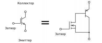
Graphic designations of transistors on diagrams
The line between the drain and source connections represents the semiconductor channel. If the diagram showing MOSFET transistors is represented by a thick solid line, then the element operates in depletion mode. Since the drain current can flow at zero gate potential. If the channel line is shown as a dotted or broken line, then the transistor operates in saturation mode, since current flows at zero gate potential. The direction of the arrow indicates the conductive channel, p-type or n-type semiconductor device. Moreover, domestic transistors are designated in exactly the same way as their foreign counterparts.
Inverse mode (3rd quadrant)
In inverse mode, the MOSFET acquires a diode characteristic at the cutoff voltage VGS(th) (Fig. 11). This behavior is due to the presence of a parasitic diode in the structure; a forward voltage drop is formed at the “collector–(source)–base–(drain)–pn junction” transition. The bipolar current passing through the diode determines the behavior of the MOSFET in inverse operating mode when the channel is closed (Fig. 12a).
Rice. 12. Inverse mode MOSFET [12]: a) closed channel (bipolar current); b) open channel and low negative voltage VDS (unipolar current); c) open channel and high negative voltage VDS (combined current)
Dynamic characteristics
The dynamic properties (switching speed, losses) of MOSFET modules depend on the features of their structure, the magnitude of parasitic junction capacitances and terminal resistance. Unlike the “ideal” switch, controlled by an insulated gate without power loss, controlling a real MOSFET consumes the energy necessary to recharge the input capacitors. Obviously, the control power depends on the size of these capacitors and the switching frequency.
In addition, the switching process is influenced by parasitic inductances of the power connections inside the transistor and external switching circuits. Their presence leads to the formation of voltage surges when turned off, as well as oscillations in parasitic circuits.
The behavior of MOSFET switches in pulsed operating mode can be analyzed using an equivalent circuit:
- When the transistor is turned off, the capacitance CGD is small and approximately equal to CDS.
- When the transistor is turned on, the capacitance CGD increases rapidly from the moment the control signal VGS exceeds the drain-source voltage, the reason for this is the inversion of the layer under the gate region.
- The technical characteristics, as a rule, indicate the values of the capacitances Ciss, Cres, Coss of the switched-off transistor (Table 2).
Table 2. Small Signal MOSFET Capacitances
| Input capacitance | Ciss = CGS+CGD |
| Reverse capacitance (Miller) | Cres = CGD |
| Output Capacitance | Coss = CGD+CDS |
Small-signal MOSFET capacitance values are not of much practical significance since they are very dependent on the operating voltage (this was described in detail earlier). The behavior of the MOSFET in the “hard” switching mode of an active-inductive load with a continuous current (when the load time constant L/R is much greater than the operating frequency period) is described below. The main diagrams of currents and voltages, by analogy with the processes discussed earlier for IGBT, are shown in Fig. 13.
In addition to the “non-ideal” parameters of transistors and diodes, switching losses and the position of the operating point are significantly influenced by passive distributed elements of the switching circuit.
Inclusion
As shown in Fig. 13, the drain-to-source voltage of the power MOSFET drops to saturation level in about 10 ns, its value is determined by the formula VDC(on) = ID × RDS(on).
During the time interval 0–t1, the transistor remains blocked. Gate current IG begins to flow when the control signal appears, it charges the capacitance CGS until the charge on it reaches the level QG1. The voltage VGS increases linearly with a time constant determined by the CGS and the gate resistor RG. Since the control signal level is still below the VGS(th) threshold, the MOSFET channel remains closed.
In the time interval t1–t2, the drain current ID begins to increase when the gate voltage reaches the level VGS(th) (time t1). The ID value is related to the control signal through the transconductance gfs (ID = gfs × VGS), and the gate voltage is increased to the value VGS1 = ID/gfs (t2). Since the opposed diode can block the flow of current only at time t2, the voltage VDS before this decreases insignificantly. At t = t2, the gate charge reaches the value QG2.
During this time interval, the largest part of the turn-on losses Eon is generated in the transistor. As long as ID < IL and some of the current IL still continues to flow through the box diode, the level of VDS cannot become much lower than the supply voltage VDD. The difference between VDD and VDS, marked in Fig. 13, is mainly caused by transient dynamic signal drop on the parasitic inductances of the switching circuit.
The time interval t2–t3 corresponds to a fully turned on transistor. When the box diode is turned off, the drain-source voltage drops to the saturation level VDS(on) = ID×RDS(on). Between times t2 and t3, the drain current and gate voltage are still coupled through the transconductance parameter, and VGS remains virtually unchanged. After the MOSFET turns on, the gate current IG discharges the Miller capacitance to the level (QG3–QG2). At t = t3, an amount of charge equal to QG3 remains on the gate. When all the load current IL begins to flow through the open channel of the MOSFET, the box diode begins to turn off. The reverse recovery process of the diode causes the drain current ID to exceed IL by an amount IRR (reverse recovery current) during time trr, and the transistor dissipates additional energy due to the charge Qrr.
The time interval t3–t4 corresponds to the ohmic region of the characteristic. At moment t3, the transistor is turned on, its operating point has passed the active zone and reached the boundary of the ohmic working region. The control signal VGS is no longer coupled to the current ID through the transconductance gfs. The accumulation of gate charge (QGtot–QG3) leads to a further increase in VGS, reaching the level of the output voltage of the driver VGG.
Shutdown
When the field effect transistor is turned off, all processes occur as described above, but in reverse order. The charge QGtot must be absorbed by the reverse gate current, and, unlike IGBTs, power MOSFETs do not need to be turned off with a negative voltage (VGSoff = 0). During the shutdown process, it is necessary to discharge only the MOSFET's own capacitances to a level where the influence of charge carriers on the channel region ceases.
The drain overvoltage noted in Fig. 13 at the moment of switching off, is caused by the presence of parasitic inductances in the switching circuit, its level is proportional to the rate of current decay dID/dt.
Rice. 13 . Diagrams of currents and voltages in the “hard” switching mode of MOSFET and IGBT with an opposed diode to an active-inductive load
The more a MOSFET's switching behavior deviates from "ideal hard switching", the more distorted the gate step response becomes.
Development support
The company's website provides a library of temperature models (R‑C thermal Model Parameters) for most manufactured field-effect transistors. To facilitate the design of printed circuit boards, the developer is provided with a library of ready-made footprints for all types of field-effect transistor packages, which allows one to avoid errors that arise when creating a footprint independently. There is a library of Spice models for a wide range of transistors. To simulate the behavior of high-power MOSFETs, Vishay Siliconix has developed a new version of the ThermaSim 3.0 software simulator, with a time resolution of up to 1 ns, which significantly improves the reliability of the design process.
Literature
- SiZ916DT Dual N‑Channel 30 V (D‑S) MOSFETs. Datasheet Vishay Siliconix. 2012.
- Power MOSFETs. Medical Approved Process Flow and Devices for Implantable Applications. Vishay Siliconix. 2012.
- Automotive level qualification requirements for discrete products. (Per AEC-Q101). 2010.
- Power MOSFETs. PolarPAK. Vishay Siliconix. 2012.
- Hi-Rel Components. Long-Time Supplier for High-Reliability Applications. Vishay Siliconix. 2012.
- SkyFET. Integrated MOSFET and Schottky Diode Solution. 2012.
- 1.2 V Rated MOSFETs. Industry's First Load Swit-ches Designed for On-Resistance Ratings at 1.2 V. 2012.
- Battery Disconnect Switch. Vishay Siliconix. 2011.
The latest generations of MOSFETs and the main directions for their improvement
Power electronics generally uses switches with a vertical structure, in which the gate and source terminals are located on the surface of the chip, and the drain terminal is located on the bottom side. In this case, the load current passes vertically through the chip. The so-called Vertical Double Diffused MOSFET, or VDMOSFET, appeared on the market in the early 80s. They are still widely used, and their improvement is proceeding along the path of reducing the cell size.
Depending on the application area and operating voltage, the development of MOSFET technology follows two main directions, the first of which is the Trench-Gate MOSFET (Fig. 14) [13]. The groove gate transistor structure was first introduced in 1997, and its improvement is still ongoing.
Rice. 14 . on the left is the structure of a standard VDMOSFET; on the right is a MOSFET with a “trench” gate (Trench MOSFET)
Like the Trench IGBT, the insulated gate and channel regions are arranged vertically, which significantly reduces the distance that electrons must travel in the n-region. As a result, it is possible to significantly reduce the RDS(on) value, especially in the low-voltage operating voltage range.
The most notable progress in improving the conduction characteristics of field-effect transistors was achieved by Infineon in 1999, when the first Superjunction MOSFETs under the CoolMOS brand appeared on the market. In these switches, the compensation principle was used to reduce channel resistance at operating voltages in the range of 500–1000 V. The structure and operating principle of CoolMOS are shown in Fig. 15 [11].
Rice. 15. Superjunction MOSFET (CoolMOS) Structure
Using multistage epitaxy or lateral trench diffusion, it is possible to inject highly doped conducting “pillars” into a lightly doped n—-drift zone. Structurally, they are connected to p-pockets. The doping level of the pillars is chosen to compensate for n impurities in the drift region, resulting in a very low effective doping level.
In the off state, the field distribution is almost rectangular, and the blocking ability is determined by the thickness of the n-zone. The doping of the drift region can only be increased to a level that is compensated by a similar amount of impurities in the p-“column”. This makes it possible to redefine the degree of mutual dependence of the magnitude of the blocking voltage and the doping density [3].
As a result, the thickness of the n—-drift region is noticeably reduced compared to a conventional MOSFET, and its conductivity, accordingly, increases due to heavy doping. This means that the on-channel resistance RDS(on) no longer has a power-law dependence on the operating voltage, as was previously the case. Using the compensation principle makes it possible to make the relationship between RDS(on) and V(BR)DSS almost linear, while the conduction losses of high-voltage MOSFETs are reduced by approximately 3–5 times. Die area, switching loss, and gate capacitance/charge are reduced accordingly; in Fig. 16 [14] shows the difference in the designs and characteristics of the standard and Superjunction MOSFET.
Rice. 16. Comparison of standard and Superjunction MOSFET
To extend the superjunction principle to low-voltage MOSFETs, it is necessary to develop a much simpler and cheaper technology than that used to produce high-voltage transistors. This problem was solved by Infineon, which developed an OptiMOS structure suitable for the production of switches with operating voltages up to 300 V [15]. Instead of “pillars,” OptiMOS transistors use isolated “field plates” that are embedded during the epitaxy process. They are located in grooves etched in the n—-drift zone and isolated by a layer of silicon oxide. The plates are alternately connected to the source and gate regions made of polycrystalline silicon (Fig. 17) [15].
Rice. 17. OptiMOS structure
In Fig. Figure 18 [15] shows the compensation effect of the field plates and the y-axis field strength response compared to a conventional blocked pn junction. The p-type charge of the "field plates" compensates for the doping of the n-band, as a result of which it can be increased, as described above.
Rice. 18. Field distribution in a conventional pn junction and a pn junction with “field plates”
In the off state, the triangular field shape in a simple MOSFET structure becomes almost rectangular, allowing the thickness of the n-layer to be reduced. Increasing the doping level and reducing the size of the drift region provides the same benefits as using the “superjunction” concept described above.
The most promising direction for improving power switches is the use of silicon carbide (SiC) technology, which is being commercially introduced into production by leading manufacturers of element base. The widespread use of SiC switches today is hampered by limited load capacity and high price. The main way to expand the current range is to increase the chip size, but this is not the best method for SiC structures, since it leads to an increase in the percentage of defective crystals and a further increase in the cost of finished products.
Full implementation of the capabilities of SiC technology allows you to increase the rated current by eliminating anti-parallel diodes (Schottky Barrier Diode, SBD) and using reverse conductivity MOSFET, as well as parallel connection of crystals without disturbing the current balance.
The bias voltage of SiC PN diodes is relatively high because silicon carbide is a wide-gap material, and this creates high conduction losses. However, the relatively high forward voltage of the internal diode can be reduced by using the reverse conduction effect of the MOS channel.
The “bipolar degradation” of SiC structures remains a serious issue. The problem with SiC PN diodes is the expansion of the defective region after operation in direct conduction mode, which leads to an increase in the open channel resistance and an increase in leakage current. ROHM was able to suppress this effect and confirm the absence of any changes in the characteristics of the solid diode over 1000 hours, which was noted in the PCIM 2012 materials.
The internal diodes of SiC MOSFETs have approximately the same reverse recovery time as SBDs, and their dynamic loss energy is lower than that of Si-MOSFETs and silicon fast diodes (Si-FRDs). The recovery current of solid diodes increases slightly at a temperature of +125 ° C, while for SBD it remains approximately the same as under normal conditions, but their reverse recovery energy is much lower than that of Si-FRD. All of the above makes it possible to create silicon carbide power modules without the use of separate antiparallel/opposite diodes.
When NTC FETs are connected in parallel, the highest current will flow through the switch with the lowest Ron value, which in the worst case will lead to thermal runaway. However, in the case of SiC MOSFETs, the risk is much lower, since silicon carbide structures have a positive temperature coefficient (at a turn-on voltage of Vgs = 18 V). Thanks to this, current equalization of parallel SiC switches in static mode occurs automatically.
However, there is a problem of unbalanced gate currents at turn-on. For silicon IGBTs, which have low internal gate resistance, the difference in parasitic inductances of the control circuits has a noticeable effect on the current distribution. In the worst case, this can lead to the destruction of silicon structures due to startup overloads and the parasitic oscillations caused by them.
Unlike Si IGBTs, silicon carbide transistors have a relatively high internal gate resistance (several ohms). Thanks to this, an acceptable distribution of control currents of parallel chips is ensured without the use of additional resistors Rg. These properties of SiC MOSFET chips make them very easy to interconnect without losing the balance of drain and gate currents, which eliminates the risk of thermal runaway or parasitic resonant oscillations.
Replacing Schottky diodes with internal MOSFET diodes allows you to increase the rated current of the module by approximately 50%. ROHM produces a 100% SiC MOSFET with a rated current of 180 A, the saturation voltage of which is 2.3 V (Ron = 12.8 mOhm). Due to the absence of tail current and the fast recovery characteristics of SiC structures, the overall switching losses are reduced by 75% compared to similar IGBTs. The use of the conduction effect of body diodes does not reduce the reliability of the module; SiC MOSFET tests have confirmed the absence of “bipolar degradation”.
What are MOSFET transistors?
A MOSFET is a voltage-controlled field-effect transistor that differs from a field-effect transistor in that it has a "metal-oxide" gate electrode that is electrically isolated from the host semiconductor by a p-channel or p-type channel with a very thin layer of insulating material. As a rule, this is silicon dioxide (or, more simply, glass).
This ultra-thin insulated metal gate electrode can be thought of as a single plate capacitor. The isolation of the control input makes the MOSFET's resistance extremely high, almost infinite.
Like field effect transistors, MOSFETs have a very high input impedance. Can easily accumulate large amounts of static charge, which can cause damage if circuits are not carefully protected.