The IGBT power transistor is controlled by voltage applied to a controlled gate electrode, which is isolated from the power circuit. Full name of the device: bipolar transistor with insulated gate.
A characteristic feature of this transistor is the very low value of control power used for switching operations of significant current values of power circuits.
Rice. No. 1. Efficiency of using technologies based on high-power IGBT transistors
Its use in power circuits for frequency converters, for alternating current motors, the power of which can reach up to 1 MW, has acquired predominant importance. In terms of its current-voltage characteristics, it is considered an analogue of a bipolar transistor, however, the quality energy indicators and the purity of switching actions are much higher than the quality of operation of other semiconductor elements.
Constantly improving technologies make it possible to improve the quality characteristics of transistors. Elements have been created that are designed for high voltages, above 3 kV, and high current values up to several hundred amperes.
Insulated Gate Bipolar Transistor
The title of this section translates to “insulated gate bipolar transistor.” This is a modern device that appeared around the end of the last century and made a revolution in power electronics. Electricity has been used by mankind for a long time; with the development of technology, one part of the emerging problems was successfully solved, such as the abandonment of expensive magnetic alloys in favor of cheap steel and copper field windings in DC motors and magnets (Werner Siemens). The other part of the problems remained stubbornly resistant to solution for a long time. This includes, for example, the use of alternating current in electric vehicles.
Electrical devices always contain switching elements and these are their most painful areas. When many electrical circuits break, an arc occurs that burns out the contacts over time. The contact resistance should ideally be no more than the smallest section of the rest of the circuit, but in practice, it is thanks to the oxides from the arc that increased resistance occurs at the contact point. According to the Joule-Lenz law, thermal power appears and dissipates at this resistance, proportional to the resistance and the square of the current. Heating of the contact point by current leads to its accelerated aging, the further, the faster, and as a result the circuit fails.
Semiconductor switches
The task of any switch in electrical engineering is to provide a short circuit. The ideal key is one that has:
- infinitely high open resistance;
- zero turn-on (closing) time;
- zero resistance in closed state;
- zero shutdown time.
Engineers have long tried to use vacuum, and various gases, and mercury, and oil, and gold with platinum, and much more, in order to make high-speed switches that are not afraid of arcs and successfully combat it. The solution was found only in semiconductor materials, which appeared by the beginning of the second half of the last century and not immediately. First, semiconductor diodes operating at industrial frequencies, then bipolar transistors, the transition from germanium to silicon, a slight increase in operating frequencies, the invention of the thyristor, jfet transistors, approximately in this way electronics went to the concept and term power transistor switch (PTS).
In their search for the perfect key to solid state physics, engineers came up with the MOSFET: “Metal-Oxide-Semiconductor Field Effect Transistor.” This is an amazing device that made the first revolution in power pulse technology. It is capable of switching significant currents simply by the presence (or absence, depending on the type) of an electric field at the gate. The current in the control circuit turned out to be unnecessary; however, when operating frequencies increased, the parasitic gate capacitance had to be fed with current, and this caused its own problems.
The disadvantages of bipolar transistors common at that time included:
- high current in the control circuit;
- low current transfer coefficient;
- strong variation of parameters from instance to instance;
- dependence of parameters on temperature;
- low permissible current density in pulsed modes;
- alternating voltage at the base for locking;
- tendency to accumulate current;
- long time of resorption of minor carriers.
As for field-effect transistors, they are free from these disadvantages due to the very principle of their design. They do not have a pn junction with all its problems. The disadvantages of the MOSFET include the rather unimportant qualities of direct conduction, especially as the operating voltage of the devices increases. Bipolar, in this regard, can have a fairly low collector-emitter voltage when on. MOSFETs have found good use in high-frequency pulse technology.
Functionality check
Inspection and testing of IGBT semiconductors is carried out in the presence of faults in electrical devices. This test is carried out using a multitester, ringing the collectors and electrodes with the emitter in two directions. This will allow you to establish the functionality of the transistor and eliminate the lack of a short circuit. When checking, it is necessary to negatively charge the gate input using COM type multimeter probes.
To check the correct operation of the transistor at the input and output of the gate, charge the capacitance with the positive pole. This charging is performed by briefly touching the gate with a probe, after which the potential difference between the collector and emitter is checked. These potentials should not have a discrepancy of more than 1.5 Volts. If a powerful IGBT is being tested, and the tester is not enough for a positive charge, a supply voltage of up to 15 Volts is applied to the gate.
IGBT transistors
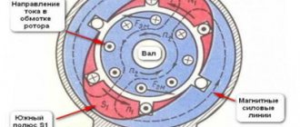
By combining the positive qualities of bipolar and field-effect transistors with an insulated gate, you can obtain a very worthy switching element for low-frequency (meaning industrial frequency 50-60 Hz) technology - IGBT.
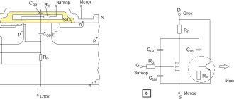
Its designation and simplified equivalent circuit are shown in the figure above. The circuit is assembled similarly to Darlington for bipolar. A field-effect transistor with an n-channel actually serves as a current amplifier with high gain, and well opens the bipolar transistor associated with it, which serves as a power transistor in this pair. Its emitter in this structure is called a collector and vice versa (according to the “duck principle” - in relation to the terminals, the device partly behaves like a bipolar transistor with a giant gain). At the same time, IGBT cannot be considered a simple circuit that is “soldered together” from n-channel field-effect and pnp bipolar transistors - this is precisely a semiconductor structure, not a circuit. The formal base-collector junction of the bipolar part and the field channel form a single structure on the crystal.
The scope of application of IGBT transistors in terms of electrical parameters lies from 300 V and above, in terms of frequency - up to 10 kHz. This is just well suited for industrial frequency (in the use of frequency generators). IGBTs are used in electric drives ranging from small power tools to electric locomotives. The fact that they operate in the region of not very high frequencies, unlike mosfet, eliminates many problems associated with parasitic inductances and capacitances - the control transistor in such a structure feels quite comfortable, its switching frequency is relatively low. This means it is easier to reload the bolt capacitance.
In this case, high conductivity is not required from it. The output PNP bipolar transistor is designed in such a way that it can withstand high reverse voltage and can operate in inverse mode. The ease of control of IGBTs and the range of safe operation turned out to be much higher than that of bipolar transistors. IGBTs, as such, do not have a built-in flyback diode, but such a fast recovery diode can be added to the circuit either externally or integrated on-chip if needed for the application for which the device is intended.
IGBTs appeared in 1983 (the first sample was patented in IR). The first samples did not switch well and were unreliable, so they did not enter the market properly. The difficulties were technological, related to obtaining plates with a thickness of about 100 microns. Overcoming them, as well as the emergence of Trench technology for the manufacture of MOSFETs, made it possible to sharply reduce the channel resistance in the open state, and this made it possible to bring the properties of IGBT closer to the properties of a traditional mechanical switch, but without the inherent arcing and with several orders of magnitude high performance.
IGBT transistors are used in frequency converters and soft starters; they are rapidly replacing thyristors in all areas, despite their significant price. It is used in power supplies, inverters, electric drives, welding power devices, and in transport.
History of appearance
The first field-effect transistors were developed in 1973, and 6 years later, controlled bipolar models appeared that used an insulated gate. As technology has improved, the efficiency and quality of operation of such elements have significantly improved, and with the development of power electronics and automatic control systems, they have become widespread, found today in almost every electrical appliance.
Today, second-generation electronic components are used that are capable of switching electric current in the range of up to several hundred Amperes. The operating voltage of IGBT transistors ranges from hundreds to thousands of volts. Improving electrical manufacturing technologies make it possible to produce high-quality transistors that ensure stable operation of electrical appliances and power supplies.
IGBT modules
Since IGBTs, as a rule, are extremely rarely used in a single version, designers began to think about modular options for their layout. The module is much simpler and more compact to use in products. But not only that.
A very important function of IGBT modules is the ability to increase the power of frequency converters and inverters without large material costs!
A low-power frequency converter with advanced control functions costs much less than a powerful one. A powerful IGBT module is not cheap in itself, but a powerful IGBT module and an inexpensive but “smart” frequency converter can be several times cheaper in price. Consumers (and producers) have a lot to think about.
However, the intervention of sufficiently qualified engineers will be required, since we are talking about reworking the frequency circuit, since not all models allow such an expansion: there are no outputs for such connections, and not a word in the instructions, except, perhaps, a ban on interfering with converter diagram on the consumer side and disclaimer for such cases. In addition to the technical side of the matter, there is also a possible legal one: possible violation of patents, licenses, etc. This should also be kept in mind.
Scope of use
Today, IGBT transistors are used in networks with voltage ratings up to 6.5 kW, while ensuring safe and reliable operation of electrical equipment. It is possible to use an inverter, variable frequency drives, welding machines and pulse current regulators.
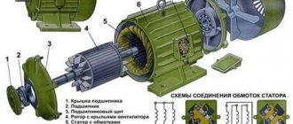
Heavy-duty IGBT varieties are used in powerful control drives for trolleybuses and electric locomotives. Their use makes it possible to increase efficiency, ensuring the smoothest possible operation of equipment, promptly controlling the output of electric motors to their full power. Power transistors are used in high voltage circuits. They are used in circuits for household air conditioners, dishwashers, power supplies in telecommunications equipment, and in automobile ignitions.
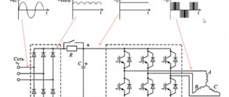
IGBT module for frequency converter
IGBT modules are connected to the control circuit using drivers, since the modules do not have built-in drivers. These are special integrated circuits that allow you to effectively drive IGBT gates and extract maximum efficiency from them. The main thing for which drivers are needed is to reduce the switching times of IGBTs to the limit, and thereby bring them closer to the ideal switch from electrical engineering textbooks. Then, coordinate them electrically with the control circuit, including providing galvanic isolation if necessary.
If external IGBT modules are used to amplify the frequency converter, then all that remains is to connect the driver outputs to them. The module diagram for the frequency converter is shown below:
The module is screwed onto a cooling aluminum radiator through heat-conducting lead paste or special ceramic gaskets. These surfaces must lie strictly in the same plane and be completely clean during assembly! Otherwise, sufficient heat dissipation will not be ensured. By the way, about temperature. The module has a built-in thermistor temperature sensor (terminals 22 and 23). The operating temperature in the module should not exceed 100°C. To remove sufficient current, additional loops are made on the power contacts (the module is made for soldering).
Contacts 1,2,3; 4,5,6; 7,8,9 are connected to a three-phase supply network.
Contacts 38,39,40 are the positive bus of the network rectifier, and contacts 41,42,43 are negative.
Contacts 33,34,35 are the positive bus of the output inverter bridge, and contacts 30,31,32 are negative. The last four listed groups, as well as pin 29, group 36,37 form the outputs for the DC link.
Contacts 10, 28 are used to connect to the driver that controls the operation of the output phase of the frequency converter. A similar role is played by groups 14, 26 and 18, 24 for the two remaining phases. Contacts 11, 12, 13 are the output of one phase of the inverter, and groups 15,16,17 and 19,20,21 are the outputs of the other two phases.
Correct PWM timing diagrams and sufficient efficiency of the drivers, which must cope with the charging and discharging of the transistor's gate capacitance, are the key to the fact that the motor will rotate at all and nothing will burn out. Therefore, the inverter bridge must first be powered from a low-power DC source with current limitation and make sure, using an oscilloscope, that there are no through currents, that the “sine” generated by the bridge is correct, that the phase shift is correct, at all frequencies that the converter produces. The control power in the frequency converter is also supplied in a laboratory manner.
The module temperature feedback signal must also be correct. When heating the module in any way within 20...80°C, it is necessary to control its actual temperature with an accurate thermometer. Then find the item with the corresponding parameter in the converter menu and check it.
If we make sure that the drivers reliably control the module, and the temperature feedback signal does not contain errors, then we can do the installation, assemble the DC link and then check again on a low-power motor, through fuses designed for the appropriate current, included in every phase.
Reasons for heating modules and the need to cool them
Since our switches are not ideal, that is, they do not provide a perfect short circuit, their resistance in the open state is not zero. This means that Joule heat is dissipated at this resistance. This is one source, and not the most significant.
In addition to the open state, there are also transient processes associated with turning on and off. During this period, the collector-emitter resistance decreases from several gOhms to units or tens of milliOhms. At the moment the key resistance is equal to the resistance of the rest of the circuit, the dissipated power reaches its maximum. Then the power drops to the open state level. The result is a power impulse. If we integrate it over the period of time during which the switching process occurs, we will find the thermal energy of this pulse.
When turned off, something similar happens, but in the opposite direction. Losses in the control circuit, against the background of losses in the power circuit, look like toys; they can be neglected (these are not problems for consumers, but for developers). Public key losses are an academic concept, but in practice they are absolutely zero. The IGBT switch-on and switch-off pattern is clearly shown below.
V(GE) is the gate-emitter voltage, I(C) is the collector current.
When the IGBT is turned on, a current pulse occurs, and when turned off, a voltage pulse occurs due to the inductive nature of the load. The dynamic range can be quite significant, but the transient speed is quite small. To suppress reverse voltage surges, you need pulsed high-speed diodes, which, in turn, also require fast recovery. IGBTs switch with the frequency of the PWM modulator, which is a few or more than ten kHz.
The higher the modulation frequency is chosen, the more accurately the sinusoid can be reproduced, but the greater the switching losses, the more the module heatsink heats up and the more radio interference occurs. The lower the modulation frequency, the easier it is for the IGBT module to operate, but the greater the current harmonics in the power circuit and its reactive power. Therefore, the consumer is given the opportunity to choose the PWM modulation frequency within the range of 2...16 kHz (different models of frequency generators have different ranges) with a discrete step of several steps.
The heatsinks of IGBT modules can dissipate power from a few W to several kW, depending on the power of the modules. In general, we can assume that modern IGBT modules dissipate about 0.3...0.5% of switched power into heat. This is quite good compared to the technology of previous years.
Key Features and Benefits of IPM
Peculiarities
- 600V three-phase IGBT bridge inverter including switch control IC and freewheeling diodes
- IGBT short circuit protection
- Fully insulated housing made using DBC technology with increased heat dissipation
- Smart shutdown function
- Comparator for protection against current exceeding the maximum permissible value during a short circuit
- Operational amplifier to increase the sensitivity of the current sensor
- Built-in limiting diodes
- Small form factor
Advantages
- Convenient microcontroller control
- High efficiency and reliability
- Very low thermal resistance Rth
- Reduced number of components
- Optimized PCB topology
- Reduced PCB size (compact design)
- Low failure rate
- Ease of implementation of the field-driven control (FOC) algorithm without the use of additional sensors
Table 4 presents the main characteristics of ST's IPM.
Table 4. Main characteristics of ST intelligent power modules (IPMs)
| Peculiarities | Basic version | Full featured version | |||
| STGIPS10K60A | STGIPS14K60 | STGIPL14K60 | STGIPS20K60 | STGIPL20K60 | |
| Operating voltage, V | 600 | 600 | 600 | 600 | 600 |
| Operating current at TC=25 °C, A | 10 | 14 | 15 | 18 | 20 |
| RthJC max. For one IGBT, °C/W | 3,8 | 3 | 2,8 | 2,4 | 2,2 |
| Type of shell | SDIP-25L | SDIP-25L | SDIP-38L | SDIP-25L | SDIP-38L |
| Case size, mm (X, Y, Z) | 44,4×22,0×5,4 | 44,4×22,0×5,4 | 49,6×24,5×5,4 | 44,4×22,0×5,4 | 49,6×24,5×5,4 |
| DBC technology | Yes | Yes | Yes | Yes | Yes |
| NTC | Yes | Yes | Yes | Yes | Yes |
| Built-in limiting diodes | Yes | Yes | Yes | Yes | Yes |
| SD function | No | Yes | Yes | Yes | Yes |
| Comparator for short circuit protection | No | Yes (1 output) | Yes (3 pins) | Yes (1 output) | Yes (3 pins) |
| Smart shutdown function | No | Yes | Yes | Yes | Yes |
| Operational amplifier to increase the sensitivity of the current sensor | No | No | Yes | No | Yes |
| Mutual shutdown function | Yes | Yes | Yes | Yes | Yes |
| Overvoltage lockout | Yes | Yes | Yes | Yes | Yes |
| Open emitter configuration | Yes (3 pins) | Yes (3 pins) | Yes (3 pins) | Yes (3 pins) | Yes (3 pins) |
| Compatible with 3.3/5V logic input levels | Yes | Yes | Yes | Yes | Yes |
| Input signal for high-side IGBTs | High active level | High active level | High active level | High active level | High active level |
| Input signal for low-side IGBTs | High active level | Low active level | Low active level | Low active level | Low active level |