Silicon crystal lattice
In the normal state, silicon atoms form a crystal lattice
.
There are four electrons in the outer electron shell of an atom. With their help, a covalent bond
with four neighboring atoms. Each electron in such a bond belongs to two atoms at the same time. Thus, each atom has eight electrons in its outer electron shell. As a result, since the last level of the electron shell is complete, it is very difficult to remove its electrons from the atom and the material behaves like a dielectric (does not conduct electric current).
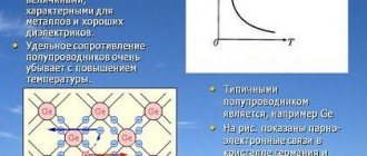
Dependence of semiconductor conductivity on temperature and illumination
Semiconductors are substances whose resistance decreases with increasing temperature, changes in illumination, and the presence of impurities.
When a semiconductor thermistor is heated, the current in the circuit increases, which indicates a decrease in its resistance.
When a semiconductor photoresistor is illuminated, the current in the circuit increases, which indicates a decrease in its resistance.
Typical semiconductors are germanium (Ge) and silicon (Si) crystals.
Types of semiconductor conductivity
Electronic conductivity
Let's add a pentavalent arsenic atom (As) to a silicon semiconductor. Through four valence electrons, arsenic will establish covalent bonds with four neighboring silicon atoms. There will be no pair left for the fifth valence electron and it will become weakly bound to the atom.
Under the influence of an electromagnetic field, such an electron is easily torn off and is drawn into the ordered movement of charged particles (electric current). An atom that has lost an electron turns into a positively charged ion with a free vacancy - a hole.
Despite the presence of holes in a silicon semiconductor with an admixture of arsenic, the main carriers of free charge are electrons. Such conductivity is called electronic, and a semiconductor with electronic conductivity is called an N-type semiconductor.
Hole conductivity
Let us introduce a trivalent indium atom (In) into the silicon crystal. Indium will establish covalent bonds with only three neighboring silicon atoms. For the fourth “neighbor”, indium is missing one electron. This missing electron can be captured by an indium atom from the covalent bond of neighboring silicon atoms.
The indium atom turns into a negatively charged ion, and a vacancy (hole) is formed in the covalent bond of neighboring atoms. In turn, an electron from a neighboring covalent bond can jump to this place. The result is a chaotic wandering of holes throughout the crystal.
If you place a semiconductor in an electromagnetic field, the movement of holes will become ordered, i.e. an electric current will occur. Thus, hole conductivity is ensured. A hole-conducting semiconductor is called a P-type semiconductor.
What is a semiconductor and what is it eaten with?
Semiconductor is a material without which the modern world of technology and electronics is unthinkable. Semiconductors exhibit properties of metals and non-metals under certain conditions. In terms of electrical resistivity, semiconductors occupy an intermediate position between good conductors and dielectrics. A semiconductor differs from conductors in the strong dependence of specific conductivity on the presence of impurity elements (impurity elements) in the crystal lattice and the concentration of these elements, as well as on temperature and exposure to various types of radiation. Basic property of a semiconductor
- increase in electrical conductivity with increasing temperature. Semiconductors are substances whose band gap is on the order of several electron volts (eV). For example, diamond can be classified as a wide-gap semiconductor, and indium arsenide can be classified as a narrow-gap semiconductor. The band gap is the width of the energy gap between the bottom of the conduction band and the top of the valence band, in which there are no allowed states for the electron. The magnitude of the band gap is important when generating light in LEDs and semiconductor lasers and determines the energy of the emitted photons.
Semiconductors include many chemical elements: Si silicon, Ge germanium, As arsenic, Se selenium, Te tellurium and others, as well as all kinds of alloys and chemical compounds, for example: silicon iodide, gallium arsenide, mercury tellurite, etc.). In general, almost all inorganic substances in the world around us are semiconductors. The most common semiconductor in nature is silicon, which, according to rough estimates, makes up almost 30% of the earth's crust.
Depending on whether an atom of an impurity element gives up an electron or captures it, impurity atoms are called donor or acceptor atoms. The donor and acceptor properties of an atom of an impurity element also depend on which atom of the crystal lattice it replaces and in which crystallographic plane it is embedded. As mentioned above, the conductive properties of semiconductors strongly depend on temperature, and when the temperature reaches absolute zero (-273 ° C), semiconductors have the properties of dielectrics.
Semiconductor devices and their applications
Semiconductor diode
A device that uses a pn junction is called a semiconductor diode.
Electric current through a pn-type semiconductor contact:
Significant current is flowing.
There is practically no current.
Current-voltage characteristic of pn junction.
The right part of the graph corresponds to the forward direction of the current, and the left part corresponds to the reverse direction.
The semiconductor diode is used as an AC rectifier.
Transistor
The transistor has two pn junctions and is used as a power amplifier in radio electronic devices. A transistor consists of two p-type semiconductors and one n-type or two n-type semiconductors and one p-type. These junctions divide the semiconductor into three regions called emitter, base, and collector.
Integrated circuits
Based on semiconductor crystals, integrated circuits are created in which hundreds of thousands of elements are connected into a single electrical circuit.
Semiconductors are used to create:
photoresistors , which are used in automatic light switches, indicators on satellites;
thermistors used to measure temperature, in fire alarms, time relays;
photocells used in solar panels;
photodiodes , used to measure light intensity;
phototransistors used in various sensors;
LEDs used as a source of infrared radiation, sign indicators, semiconductor lasers.
Summarize
Semiconductors in electrical conductivity occupy an intermediate position between dielectrics and conductors. Semiconductors include a large group of substances (Si, Ge, etc.). Unlike metals, the resistivity of semiconductors decreases with increasing temperature .
The conductivity of semiconductors is due to the presence of free electrons and holes . In a pure crystal, electrons and holes are present in equal numbers. Such a semiconductor has its own conductivity .
When impurities are present in semiconductors, impurity conductivity . When a donor impurity with a valence one unit greater than that of the semiconductor is added, one electron remains free. n-type semiconductor .
If we add an acceptor impurity with a valence one unit less than that of the semiconductor, then in such a semiconductor the concentration of holes exceeds the concentration of electrons. p-type semiconductor .
The area of contact between two types of semiconductors is called a p- n junction . An important property of a pn junction is its one-way conductivity . This property is used in the operation of a semiconductor diode.
Semiconductors are used to create transistors, thermistors, LEDs, photocells, and integrated circuits.
Currently, semiconductor devices are widely used in radio engineering, automation, computer technology, and telemechanics.
Structure of semiconductor atoms.
Germanium and silicon are the main materials of many semiconductor devices and have four valence electrons
.
germanium atom
consists of 32 electrons, and the
silicon
of 14. But only
28
electrons of the germanium atom and
10
electrons of the silicon atom, located in the inner layers of their shells, are firmly held by the nuclei and never come off from them.
Only four
valence electrons of the atoms of these conductors can become free, and even then not always.
And if a semiconductor atom loses at least one electron, then it becomes a positive ion
.
In a semiconductor, the atoms are arranged in a strict order: each atom is surrounded by four
the same atoms. Moreover, they are located so close to each other that their valence electrons form single orbits passing around neighboring atoms, thereby linking the atoms into a single whole substance.
Let us imagine the relationship of atoms in a semiconductor crystal in the form of a flat diagram. In the diagram, red balls with a plus symbol, conventionally, indicate atomic nuclei
(positive ions), and the blue balls are
valence electrons
.
Here you can see that around each atom there are four
exactly the same atoms, and each of these four has a connection with four other atoms, etc.
Each atom is bound to each neighboring atom by two
valence electrons, with one electron being its own and the other borrowed from the neighboring atom.
Such a bond is called two-electron or covalent
.
In turn, the outer layer of the electron shell of each atom contains eight
electrons:
four
of their own, and
one each
borrowed from four
neighboring
atoms.
Here you can no longer distinguish which of the valence electrons in the atom is “yours” and which is “foreign”, since they have become common. With such a connection of atoms in the entire mass of a germanium or silicon crystal, we can consider that the semiconductor crystal is one large molecule
. In the figure, pink and yellow circles show the connection between the outer layers of the shells of two neighboring atoms.
Electrical conductivity of a semiconductor.
Consider a simplified drawing of a semiconductor crystal, where atoms are represented by a red ball with a plus, and interatomic bonds are shown by two lines symbolizing valence electrons.
At temperatures close to absolute zero, a semiconductor does not conduct
current, since there are no
free electrons
.
But with increasing temperature, the connection of valence electrons with atomic nuclei weakens
and some of the electrons, due to thermal movement, can leave their atoms.
An electron released from an interatomic bond becomes “ free
”, and where it was before, an empty space is formed, which is conventionally called
a hole
.
The higher
temperature of the semiconductor, the
more
free electrons and holes it becomes.
As a result, it turns out that the formation of a “hole” is associated with the departure of a valence electron from the shell of an atom, and the hole itself becomes a positive
electric charge equal to
the negative
charge of the electron.
Now let's look at the figure, which schematically shows the phenomenon of current generation in a semiconductor
.
If you apply some voltage to the semiconductor, the “+” and “-” contacts, then a current will arise in it. Due to thermal phenomena
, in a semiconductor crystal, a certain number of electrons will begin
to be released
(blue balls with arrows).
Electrons, attracted by the positive
pole of the voltage source, will
move
towards it, leaving behind
holes
that will be filled with other
released electrons
.
That is, under the influence of an external electric field, charge carriers acquire a certain speed of directional movement and thereby create an electric current
.
For example: the released electron closest to the positive pole of the voltage source is attracted
this pole.
By breaking an interatomic bond and leaving it, an electron leaves
behind
a hole
.
Another released electron, which is located at some distance
from the positive pole, is also
attracted
by the pole and
moves
towards it, but
when it encounters
a hole on its way, it is attracted into it
by the nucleus
of the atom, restoring the interatomic bond.
The resulting new
the hole after the second electron
is filled by
the third released electron located next to this hole (Figure No. 1).
In turn, the holes
located closest to
the negative
pole are filled with other
released electrons
(Figure No. 2). Thus, an electric current arises in the semiconductor.
While there is an electric field
, this process
is continuous
: interatomic bonds are broken - free electrons appear - holes are formed. The holes are filled with released electrons - interatomic bonds are restored, while other interatomic bonds are broken, from which electrons leave and fill the next holes (Figure No. 2-4).
From this we conclude: electrons move from the negative pole of the voltage source to the positive, and holes move from the positive pole to the negative
.