History of the development of the first transistors
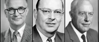
Tendencies are inherited, as seen in the example of William Bradford Shockley. The son of a mining engineer and one of the first female surveyors in the United States. A specific combination. At the age of 22 he received a bachelor's degree, did not stop there, and in 1936 he became a doctor of philosophy. The title, awarded by the Massachusetts Institute of Technology, does not mean that Shockley studied Nietzsche and Aristotle. The degree indicates the presence of a dissertation in a field from a large list of sciences. The outlandish name is a tribute to the tradition when philosophy in the Middle Ages dealt with a wide range of issues, rightfully considered the progenitor of other directions in the course of scientific thought.
Bell Labs
The purpose of the work was to study the electronic levels of sodium chloride. The band theory, which explained the processes occurring in materials, was just gaining popularity. According to the views of the theory, any electron in a crystal is capable of occupying a unique state, characteristic exclusively of the specified particle, with a certain energy and spin direction. According to the presentation, the gradations occur with some discreteness in the valence band (associated with the nucleus); in addition, there is a forbidden region where particles are not allowed to be located. The exception to the last thesis is considered to be impurity semiconductors, which have become the basis for the creation of solid-state electronics, including bipolar transistors.
Shockley came to Bell Labs for his interesting ideas in the field of nuclear reactor design. Uranium in its pure form was discovered long before this; for the first time, Becquerel discovered radioactivity using the element as an example. Enrico Fermi tried to bombard metal nuclei with neutrons in the early 30s (20th century), with the goal of obtaining transuranium elements. Later it was proven that radioactive decay occurs simultaneously with the release of energy. Shockley planned to bomb U-235 to obtain a new source of high power. During World War II, he conducted research to assess a possible Japanese land invasion, the data collected greatly contributed to Truman's decision to drop the atomic bomb on Hiroshima.
Bell Labs set Shockley a direct task - to find an alternative to bulky tube amplifiers. This would mean saving space and the birth of a new generation of devices capable of functioning in war conditions. It is no secret that the military merits of the USSR were appreciated on the opposite side of the ocean. Shockley was appointed manager of the team working on the task, which included, among other things, the creators of the first point-point transistor:
- John Bardeen;
- Walter Houser Brattain.
Readers already know about a point diode based on a crystal detector, but what was the transistor? This is a field device: two electrodes are applied to the region of the p-type semiconductor and separated by a dielectric wedge. The thickness of the barrier layer varies from base to base. A control electrode applied to the n-region at a positive potential greatly depletes the junction region, and no current flows. Historically, the first transistor is considered to be a field-effect transistor.
The design turned out to be specific. For example, gold contact pads are pressed by a spring to a germanium pn-junction crystal, more reminiscent of a laboratory installation than a fully functional device for military equipment. Assembled using paper clips and toxic electrolyte glue. But the device will in the future give its name to Silicon Valley. There was discord between scientists because Shockley's field theory, used in the transistor, did not help create the device, and was also mentioned in Lilienfeld's 1925 Canadian patent. As a result, Bell Labs removes William's name from the list of creators when completing the paperwork.
Notably, the MESFET (field-effect transistor) structure proposed by Lilienfeld did not function. But the bureau accepted the ideas, and Bell Labs had difficulty submitting applications. It’s a paradox, but scientists could only patent the design of Bardeen and Brattain - nothing more. The rest had long existed in the form of a concept at the time of 1946. Shockley decided that fate had played another joke on the inventor after all the failures. However, the Bell company makes all sorts of concessions, and it is generally accepted that William appears for the press as the first person.
William Bradford Shockley
Shockley begins to work on his own direction, while trying to correct the situation. The latter does not give positive results, but the first leads to the creation of a device today known to the world under the name of a bipolar transistor. Going through a number of designs, on January 1, 1948, he finds the correct one, but does not immediately realize it. Subsequently, Shockley came up with the idea that the current is formed not only by the main charge carriers.
Transformation of computer technologies
The invention of transistors was also revolutionary in the miniaturization of computers. Like earlier electronic devices, first-generation computers used vacuum tubes as switches and amplifiers. After the advent of transistors, manufacturers also used the small devices to create smaller, more efficient computers. In subsequent years, vacuum tubes were completely replaced by transistors, leading to the second generation of transistor computers.
The first computer to use transistors was the University of Manchester Transistor Computer. The transistor computer was built as a prototype, consisting of 92 contact point transistors and 550 diodes, and was fully operational in 1953. In 1955, a full-size version of this computer was introduced, featuring transistors with 200 contact points and 1,300 diodes. Although most of the circuits used transistors, the device was not considered a fully transistorized computer because its clock generator still used vacuum tubes.
In the mid-1950s, similar machines began to appear. The University of Manchester design was later adopted by Metropolitan-Vickers, which produced seven machines using bipolar junction transistors in 1956. However, the device, called Metrovick 950, was not commercially available and was only used internally. Similarly, Bell Labs invented the TRADIC device in 1954, but as with the transistor computer, TRADIC used vacuum tubes as clock power.
The Burroughs Atlas Mod 1-J1 control computer, built for the US Air Force in 1955, was the first computer to eliminate the use of vacuum tubes entirely, and this model was the first all-transistor computer. MIT also developed the TX-0, its own transistor computer in 1956. Transistorized computers also began to appear in other parts of the world. The first device to appear in Asia was the Japanese ETL Mark III, released in 1956. The DRTE, released in 1957, and the Austrian Mailüfterl, released in 1958, were the first transistorized computers in Canada and Europe, respectively. In 1959, Italy also released its first transistor computer, the Olivetti Elea 9003, which later became available on the private market.
Read 7 Best All-in-One Desktops of 2022
Although transistorized computers appeared worldwide in the 1950s, they were not commercially available until 1959, when General Electric released the General Electric 210. Consequently, other manufacturers also introduced their own flagship transistor computer models. The IBM 7070 and RCA 501 were among the first models released, among others. Large-scale computers also followed this trend. The Philco deal models S-1000 and S-2000 were one of the first commercially available large-scale transistor computers.
Advances in transistor design led to major changes in computer design. The production of transistor-based computers grew over time as the technology became available in the market. Eventually, integrated circuits were adopted in the 1960s, giving way to the third generation of computers.
Operating principle of a bipolar transistor, temperature conditions
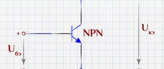
The concept Shockley outlined sends the team into a frenzy: for years he worked behind the backs of his colleagues! But the idea turned out to be successful. If the thickness of the base semiconductor is small, the injected minority charge carriers are partially captured by the collector field. There they already become the main ones, participating in the creation of electric current. The process is controlled by the base field; the number of charge carriers that break through is proportional to the applied voltage.
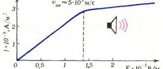
In fact, the collector pn junction operates in breakdown mode. Temperature conditions are entirely determined by the materials. Germanium transistors are not able to function at temperatures above 85 degrees Celsius, and once exceeding the reference value, subsequent cooling will not return the device to functionality. Silicon can withstand almost twice as much heat. There are often instances of transistors that can operate at 150 degrees Celsius, but the disadvantage is a relatively large voltage drop across the pn junction.
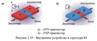
Bipolar transistor
It turns out that the designer is looking for the most suitable transistors to create an electrical circuit according to the existing conditions. The power dissipation is calculated, and if necessary, the elements are supplemented with massive radiators. The maximum temperature is selected with a fair margin to prevent overheating. Semiconductors have obvious resistance and are used in technology exclusively to solve specific problems. For example, when creating a pn junction. Otherwise, the thicker the layer of material, the greater the losses due to active ohmic resistance. Let us give a clear example: the resistivity of germanium exceeds the value of a similar parameter of copper (metal) by 30 million times. Consequently, losses will increase (and heating) in accordance with the indicated figure.
So, the semiconductor layer is small. How to implement this in practice? Let's temporarily forget about the paper clips used in the first design and turn to modern technology. When manufacturing a bipolar transistor, the following rules are followed:
- The emitter material serves to inject the main carriers into the base, where they will be captured by the field. Therefore, semiconductors with a large specific proportion of impurities are used. This ensures the creation of a large number of free carriers (holes or electrons). The volume of the collector is slightly higher than that of the emitter, and the power dissipation is expected to be greater. This affects the cooling conditions of the device.
- In the base, the concentration of impurities is lower so that most of the injected flow does not recombine. The proportion of third-party atoms in the crystal lattice is minimal.
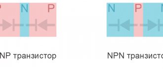
- The collector, in terms of the proportion of impurities, is located in the middle between the base and emitter. The charge carriers that break through here are required to recombine. The difference in the concentrations of impurities becomes the reason why the collector and emitter cannot be swapped in the electrical circuit of the device. The second reason is the fact that the areas of pn junctions are not the same. On the collector side – more.
Transistor action
The width of the pn junction blocking layer depends on the impurity fraction (it increases with increasing). Moreover, its penetration into the emitter, collector and base is not the same. The barrier layer extends to a minimum depth into the material with the maximum proportion of impurities. That is, the emitter. Germanium bipolar transistors are becoming a thing of the past; silicon and gallium arsenide-based ones are replacing them. Today, two technologies for the production of semiconductor devices dominate:
- Alloy transistors are produced, for example, by fusing two drops of indium of different sizes into a thin plate of germanium (mostly made from the specified material). The materials exhibit different liquidus temperatures, making furnace processing possible. Due to the diffusion of atoms, indium is firmly fused into germanium (melting point 940 degrees Celsius). Then electrodes are soldered to the emitter, collector and base.
- Planar transistors are closest to Shockley's original idea; his devices were called flat. Unlike those known before. The required layers are applied to a flat substrate using various methods. Masks of various configurations are actively used to create drawings. The advantage is the possibility of mass production of transistors on a single substrate, then it is cut into pieces, each becoming a separate semiconductor device.
During the technological manipulations described above, the stages of the production cycle are actively used:
- The diffusion method allows precise control of the geometric dimensions of the pn junction, which leads to better repeatability and accuracy. To create a transistor, a semiconductor in a gas is heated to the liquidus point, and impurities floating around easily settle on the surface. Diffusion occurs. The dosage of the partial pressure of impurity vapors and the duration of the operation varies the depth of penetration of atoms into the base material (substrate). Sometimes diffusion occurs during the fusion process. The moment is determined by precise selection of temperature conditions.
- Epitaxy is the process of growing a crystal of the desired type on a substrate. Precipitation can occur from solution or gas. Vacuum deposition also belongs to this class of technologies; electrolysis stands a little apart, based on the principle of building layers under the influence of current.
- To obtain a given mask, lithography techniques are often used. For example, a photoresist is applied to the substrate, the islands of which disappear under the action of the developer. The shaping radiation is filtered by a mask made of opaque material. The photolithography process is reminiscent of that familiar to every professional photographer who independently processes film.
Reference books often indicate two or more key terms that characterize the production cycle of a bipolar transistor.
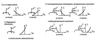
Transistor designations
external reference
- Transistor characteristics
- How do transistors work? William Beaty (in English) (in Spanish)
- Historical timeline of transistors
| Control of authorities |
|
- Datos: Q188946
- Multimedia: Bipolar junction transistors