The principle of semiconductor control of electric current was known at the beginning of the twentieth century. Even though electronics engineers knew how a transistor worked, they continued to design devices based on vacuum tubes. The reason for such distrust of semiconductor triodes was the imperfection of the first point-point transistors. The family of germanium transistors did not have stable characteristics and were highly dependent on temperature conditions.
Monolithic silicon transistors began to seriously compete with vacuum tubes only in the late 50s. Since that time, the electronics industry began to develop rapidly, and compact semiconductor triodes actively replaced energy-intensive lamps from electronic device circuits. With the advent of integrated circuits, where the number of transistors can reach billions, semiconductor electronics has won a landslide victory in the fight to miniaturize devices.
What is a transistor?
In its modern meaning, a transistor is a semiconductor radio element designed to change the parameters of an electric current and control it. A conventional semiconductor triode has three terminals: a base, which receives control signals, an emitter, and a collector. There are also high power composite transistors.
The size scale of semiconductor devices is striking - from several nanometers (unpackaged elements used in microcircuits) to centimeters in diameter for high-power transistors intended for power plants and industrial equipment. Reverse voltages of industrial triodes can reach up to 1000 V.
Device
Structurally, the triode consists of semiconductor layers enclosed in a housing. Semiconductors are materials based on silicon, germanium, gallium arsenide and other chemical elements. Today, research is being conducted to prepare certain types of polymers, and even carbon nanotubes, for the role of semiconductor materials. Apparently in the near future we will learn about new properties of graphene field-effect transistors.
Previously, semiconductor crystals were located in metal cases in the form of caps with three legs. This design was typical for point-point transistors.
Today, the designs of most flat, including silicon semiconductor devices are made on the basis of a single crystal doped in certain parts. They are pressed into plastic, metal-glass or metal-ceramic cases. Some of them have protruding metal plates for heat dissipation, which are attached to the radiators.
The electrodes of modern transistors are arranged in one row. This arrangement of the legs is convenient for automatic board assembly. The terminals are not marked on the housings. The type of electrode is determined from reference books or by measurements.
For transistors, semiconductor crystals with different structures, such as pnp or npn, are used. They differ in the polarity of the voltage on the electrodes.
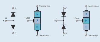
Schematically, the structure of a transistor can be represented as two semiconductor diodes separated by an additional layer. (See Figure 1). It is the presence of this layer that allows you to control the conductivity of the semiconductor triode.
Rice. 1. Structure of transistors
Figure 1 schematically shows the structure of bipolar triodes. There is also a class of field-effect transistors, which will be discussed below.
Basic operating principle
At rest, no current flows between the collector and emitter of a bipolar triode. Electric current is prevented by the resistance of the emitter junction, which arises as a result of the interaction of the layers. To turn on the transistor, you need to apply a small voltage to its base.
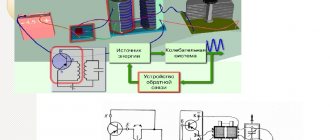
Figure 2 shows a diagram explaining the working principle of a triode.
Rice. 2. Operating principle
By controlling the base currents, you can turn the device on and off. If an analog signal is applied to the base, it will change the amplitude of the output currents. In this case, the output signal will exactly repeat the oscillation frequency at the base electrode. In other words, the electrical signal received at the input will be amplified.
Thus, semiconductor triodes can operate in electronic switch mode or in input signal amplification mode.
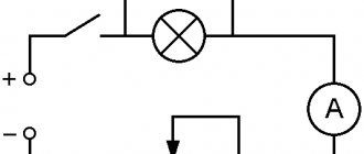
The operation of the device in electronic key mode can be understood from Figure 3.
Rice. 3. Triode in switch mode
Designation on diagrams
The generally accepted designation is “VT” or “Q” , followed by a positional index. For example, VT 3. On earlier diagrams you can find outdated designations: “T”, “PP” or “PT”. The transistor is depicted as symbolic lines indicating the corresponding electrodes, circled or not. The direction of current in the emitter is indicated by an arrow.
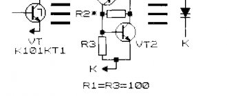
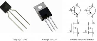
Figure 4 shows a ULF circuit in which transistors are designated in a new way, and Figure 5 shows schematic images of different types of field-effect transistors.
Rice. 4. Example of a ULF circuit using triodes
Current-voltage characteristics of the transistor
The properties of a bipolar transistor are most fully described using static current-voltage characteristics. In this case, the input and output current-voltage characteristics of the transistor are distinguished. Since all three currents (base, collector and emitter) in the transistor are closely interconnected, when analyzing the operation of the transistor it is necessary to use simultaneously the input and output current-voltage characteristics.
Each transistor switching circuit has its own current-voltage characteristics, which represent a functional dependence of the currents through the transistor on the applied voltages. Due to the nonlinear nature of these dependencies, they are usually presented in graphical form.
A transistor, like a four-terminal network, is characterized by input and output static current-voltage characteristics, showing respectively the dependence of the input current on the input voltage (at a constant value of the output voltage of the transistor) and the output current on the output voltage (at a constant input current of the transistor).
Figure 1.27 shows the static current-voltage characteristics of a pnp transistor connected in a circuit with an OE (most often used in practice).
a b
Figure 1.27 – Static current-voltage characteristics of a bipolar transistor connected according to a circuit with an OE
The input current-voltage characteristic (Figure 1.27, a) is similar to the direct branch of the diode's current-voltage characteristic. It represents the dependence of the current IB on the voltage UBE at a fixed value of the voltage UKE, that is, a dependence of the form
. (1.12)
From Figure 1.27, a it is clear: the higher the voltage UKE, the more to the right the branch of the input current-voltage characteristic shifts. This is explained by the fact that with an increase in the reverse bias voltage UCE, the height of the potential barrier of the collector pn junction increases. And since the collector and emitter pn junctions in the transistor interact strongly, this, in turn, leads to a decrease in the base current at a constant voltage UBE.
Static current-voltage characteristics, presented in Figure 1.27, a, were taken at normal temperature (20 °C). As the temperature increases, these characteristics will shift to the left, and as the temperature decreases, to the right. This is due to the fact that as the temperature rises, the intrinsic electrical conductivity of semiconductors increases.
For the output circuit of a transistor connected according to a circuit with an OE, a family of output current-voltage characteristics is constructed (Figure 1.27, b). This is due to the fact that the collector current of the transistor depends not only (and not so much, as can be seen from the figure) on the voltage applied to the collector junction, but also on the base current. Thus, the output current-voltage characteristic for a circuit with an OE is called the dependence of the current IK on the voltage UKE at a fixed current IB, that is, a dependence of the form
. (1.13)
Each of the output current-voltage characteristics of a bipolar transistor is characterized at the beginning by a sharp increase in the output current IK with an increase in the output voltage UKE, and then, as the voltage further increases, by a slight change in the current.
On the output current-voltage characteristic of the transistor, three regions can be distinguished, corresponding to different modes of operation of the transistor: the saturation region, the cutoff region and the region of active operation (amplification) , corresponding to the active state of the transistor when ½UBE ½ > 0 and ½UCE½> 0.
The input and output static current-voltage characteristics of transistors are used in graphic-analytical calculations of cascades containing transistors.
The static input and output current-voltage characteristics of a pnp-type bipolar transistor for a switching circuit with OB are shown in Figure 1.28, a and 1.28, b, respectively.
a b
Figure 1.28 – Static current-voltage characteristics of a bipolar transistor for a switching circuit with OB
For a circuit with an OB input static current-voltage characteristic, the dependence of the current IE on the voltage UEB at a fixed voltage value UKB is called, that is, the dependence is of the form
. (1.14)
The output static current-voltage characteristic for a circuit with OB is called the dependence of the current IK on the voltage UKB at a fixed current IE, that is, a dependence of the form
. (1.15)
In Figure 1.28, b, two areas can be distinguished, corresponding to two operating modes of the transistor: active mode (UKB < 0 and the collector junction is biased in the opposite direction); saturation mode (UCB > 0 and the collector junction is forward biased).
Types of transistors
Based on their operating principle and structure, semiconductor triodes are distinguished:
- field;
- bipolar;
- combined.
These transistors perform the same functions, but there are differences in the principle of their operation.
Field
This type of triode is also called unipolar, due to its electrical properties - they carry current of only one polarity. Based on their structure and type of control, these devices are divided into 3 types:
- Transistors with control pn junction (Fig. 6).
- With an insulated gate (available with a built-in or induced channel).
- MIS, with structure: metal-dielectric-conductor.
A distinctive feature of an insulated gate is the presence of a dielectric between it and the channel.
Parts are very sensitive to static electricity.
Circuits of field triodes are shown in Figure 5.
Rice. 5. Field effect transistors
Rice. 6. Photo of a real field-effect triode
Pay attention to the names of the electrodes: drain, source and gate.
Field effect transistors consume very little power. They can work for more than a year on a small battery or rechargeable battery. Therefore, they are widely used in modern electronic devices such as remote controls, mobile gadgets, etc.
Bipolar
Much has been said about this type of transistor in the subsection “Basic operating principle.” Let us only note that the device received the name “Bipolar” because of its ability to pass charges of opposite signs through one channel. Their feature is low output impedance.
Transistors amplify signals and act as switching devices. A fairly powerful load can be connected to the collector circuit. Due to the high collector current, the load resistance can be reduced.
Let's look at the structure and principle of operation in more detail below.
Combined
In order to achieve certain electrical parameters from the use of one discrete element, transistor developers invent combined designs. Among them are:
- bipolar transistors with embedded resistors and their circuit;
- combinations of two triodes (same or different structures) in one package;
- lambda diodes - a combination of two field-effect triodes forming a section with negative resistance;
- designs in which a field-effect triode with an insulated gate controls a bipolar triode (used to control electric motors).
Combined transistors are, in fact, an elementary microcircuit in one package.
How does a bipolar transistor work? Instructions for dummies
The operation of bipolar transistors is based on the properties of semiconductors and their combinations. To understand the principle of operation of triodes, let's understand the behavior of semiconductors in electrical circuits.
Semiconductors.
Some crystals, such as silicon, germanium, etc., are dielectrics. But they have one feature - if you add certain impurities, they become conductors with special properties.
Some additives (donors) lead to the appearance of free electrons, while others (acceptors) create “holes”.
If, for example, silicon is doped with phosphorus (donor), we obtain a semiconductor with an excess of electrons (n-Si structure). By adding boron (an acceptor), the doped silicon will become a hole-conducting semiconductor (p-Si), that is, its structure will be dominated by positively charged ions.
One-way conduction.
Let's conduct a thought experiment: connect two different types of semiconductors to a power source and supply current to our design. Something unexpected will happen. If you connect the negative wire to an n-type crystal, the circuit will be completed. However, when we reverse the polarity, there will be no electricity in the circuit. Why is this happening?
As a result of connecting crystals with different types of conductivity, a region with a pn junction is formed between them. Some electrons (charge carriers) from an n-type crystal will flow into a crystal with hole conductivity and recombine holes in the contact zone.
As a result, uncompensated charges arise: in the n-type region - from negative ions, and in the p-type region from positive ions. The potential difference reaches values from 0.3 to 0.6 V.
The relationship between voltage and impurity concentration can be expressed by the formula:
φ= VT * ln (Nn * Np)/n2i, where
VT is the value of the thermodynamic stress, Nn and Np are the concentration of electrons and holes, respectively, and ni denotes the intrinsic concentration.
When connecting a plus to a p-conductor and a minus to an n-type semiconductor, the electric charges will overcome the barrier, since their movement will be directed against the electric field inside the pn junction. In this case, the transition is open. But if the poles are reversed, the transition will be closed. Hence the conclusion: the pn junction forms one-way conductivity. This property is used in the design of diodes.
From diode to transistor.
Let's complicate the experiment. Let's add another layer between two semiconductors with the same structures. For example, between p-type silicon wafers we insert a conductivity layer (n-Si). It is not difficult to guess what will happen in the contact zones. By analogy with the process described above, regions with pn junctions are formed, which will block the movement of electrical charges between the emitter and collector, regardless of the polarity of the current.
The most interesting thing will happen when we apply a slight voltage to the layer (base). In our case, we will apply a current with a negative sign. As in the case of a diode, an emitter-base circuit is formed through which current will flow. At the same time, the layer will begin to become saturated with holes, which will lead to hole conduction between the emitter and collector.
Look at Figure 7. It shows that positive ions have filled the entire space of our conditional structure and now nothing interferes with the conduction of current. We have obtained a visual model of a bipolar transistor with a pnp structure.
Rice. 7. Principle of operation of the triode
When the base is de-energized, the transistor very quickly returns to its original state and the collector junction closes.
The device can also operate in amplification mode.
The collector current is directly proportional to the base current: Iк = ß*IB , where ß is the current gain, IB is the base current.
If you change the value of the control current, the intensity of hole formation on the base will change, which will entail a proportional change in the amplitude of the output voltage, while maintaining the signal frequency. This principle is used to amplify signals.
By applying weak pulses to the base, at the output we get the same amplification frequency, but with a much larger amplitude (set by the voltage applied to the collector-emitter circuit).
NPN transistors work in a similar way. Only the polarity of the voltages changes. Devices with NPN structure have direct conductivity. PNP type transistors have reverse conductivity.
It remains to add that the semiconductor crystal reacts in a similar way to the ultraviolet spectrum of light. By turning the photon flow on and off, or adjusting its intensity, you can control the operation of a triode or change the resistance of a semiconductor resistor.
Bipolar transistor connection circuits
Circuit designers use the following connection schemes: with a common base, common emitter electrodes, and connection with a common collector (Fig. 8).
Rice. 8. Connection diagrams for bipolar transistors
Amplifiers with a common base are characterized by:
- low input impedance, which does not exceed 100 Ohms;
- good temperature properties and frequency characteristics of the triode;
- high permissible voltage;
- two different power sources are required.
Common emitter circuits have:
- high current and voltage gain;
- low power gain;
- inversion of the output voltage relative to the input.
With this connection, one power source is sufficient.
The connection diagram based on the “common collector” principle provides:
- high input and low output resistance;
- low voltage gain factor (< 1).
Operating modes and transistor switching circuits
Each pn junction of the transistor can be supplied with both forward and reverse voltage. In accordance with this, there are four modes of operation of a bipolar transistor: cutoff mode, saturation mode, active mode and inverse mode.
The active mode is ensured by applying forward voltage to the emitter junction, and reverse voltage to the collector junction (the main operating mode of the transistor). This mode corresponds to the maximum value of the emitter current transfer coefficient and ensures minimal distortion of the amplified signal.
In the inverse mode, a forward voltage is applied to the collector junction, and a reverse voltage is applied to the emitter junction (ast ® min; used very rarely).
In saturation , both junctions are forward biased. In this case, the output current does not depend on the input current and is determined only by the load parameters.
In cutoff , both junctions are reverse biased. The output current is close to zero.
Saturation and cutoff modes are used simultaneously in key circuits (when the transistor is operating in switch mode).
When using a transistor in electronic devices, two terminals are needed to supply an input signal and two terminals to connect a load (receive an output signal). Since the transistor has only three terminals, one of them must be common for the input and output signals.
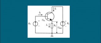
Depending on which terminal of the transistor is common when connecting the signal source and load, there are three transistor switching circuits: with a common base (CB) (Figure 1.26, a); with a common emitter (CE) (Figure 1.26, b); with a common collector (OC) (Figure 1.26, c).
In these circuits, constant voltage sources and resistors provide direct current operating modes for transistors, that is, the required voltages and initial currents. AC input signals are generated by I/O sources. They change the emitter (base) current of the transistor, and, accordingly, the collector current. Increments in the collector current (Figure 1.26, a, b) and emitter current (Figure 1.26, c) will create, respectively, voltage increments on the resistors RK and RE, which are the output signals.
a B C
Figure 1.26 – Transistor connection circuits
When determining the transistor switching circuit, it is necessary to take into account that the resistance of the constant voltage source for alternating current is close to zero.
How does a field effect transistor work? Explanation for dummies
The structure of a field-effect transistor differs from a bipolar one in that the current in it does not cross the pn junction zone. The charges move through a controlled area called the gate. The gate throughput is controlled by voltage.
The space of the pn zone decreases or increases under the influence of the electric field (see Fig. 9). The number of free charge carriers changes accordingly - from complete destruction to extreme saturation. As a result of this effect on the gate, the current at the drain electrodes (contacts that output the processed current) is regulated. The incoming current flows through the source contacts.
Figure 9. Field-effect transistor with pn junction
Field triodes with a built-in and induced channel operate on a similar principle. You saw their diagrams in Figure 5.
Field-effect transistor connection circuits
In practice, connection diagrams are used by analogy with a bipolar triode:
- with a common source - produces a large gain in current and power;
- common gate circuits provide low input impedance and low gain (has limited use);
- common-drain circuits that operate in the same way as common-emitter circuits.
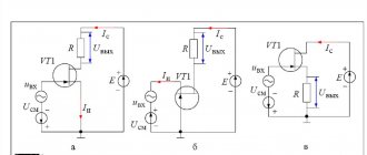
Figure 10 shows various connection schemes.
Rice. 10. Image of field triode connection diagrams
Almost every circuit is capable of operating at very low input voltages.
