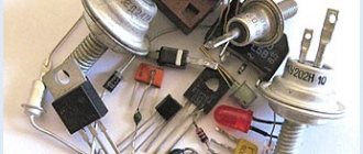
Hello dear readers of the site. The site has a section dedicated to beginner radio amateurs, but so far I haven’t really written anything for beginners taking their first steps into the world of electronics. I fill this gap, and with this article we begin to get acquainted with the structure and operation of radio components (radio components).
Let's start with semiconductor devices. But to understand how a diode, thyristor or transistor works, you need to understand what a semiconductor . Therefore, we will first study the structure and properties of semiconductors at the molecular level, and then we will deal with the operation and design of semiconductor radio components.
Semiconductor materials.
Also on topic:
ELECTRONICS INDUSTRY
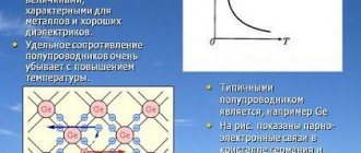
A semiconductor is a material that conducts electricity better than a dielectric such as rubber, but not as well as a good conductor such as copper. Unlike metals, the electrical conductivity of semiconductors increases with increasing temperature. The best semiconductor materials include silicon (Si) and germanium (Ge); others include compounds of gallium (Ga), arsenic (As), phosphorus (P) and indium (In). Silicon has many uses in transistors, rectifiers and integrated circuits. Gallium arsenide (GaAs) is commonly used in microwave and optoelectronic devices, as well as integrated circuits. see also
PERIODIC SYSTEM OF ELEMENTS; INTEGRATED CIRCUIT; SOLID STATE PHYSICS; TRANSISTOR.
A semiconductor is essentially a dielectric until a small and carefully measured amount of some suitable material is introduced into it. For example, a material such as phosphorus makes silicon conductive by adding excess electrons to it (i.e., acting as a “donor”). Silicon doped in this way becomes silicon n
-type.
Doping with a material such as boron transforms silicon into a p
-type material: boron (the acceptor) takes away some of the electrons from the silicon, creating “holes” in it, which can be filled with electrons from nearby atoms and thereby increase the conductivity of the doped material. (The flow of electrons in one direction and holes in the opposite direction forms a current.) The electrons and holes that thus provide conductivity are called charge carriers.
Crystal structure of semiconductors
The germanium and silicon atoms in the periodic table are in the same group as carbon (the chemical formula for diamond is C, which is simply large crystals of carbon produced under certain conditions) and therefore, when combined, form a diamond-like crystal structure. The formation of such a structure is shown, in a simplified form, of course, in Fig. 4.
Crystal structure of semiconductors (Fig. 4)
There is a germanium atom in the center of the cube, and 4 more atoms are located in the corners. The atom depicted in the center of the cube is connected with its valence electrons to its nearest neighbors. In turn, the corner atoms give up their valence electrons to the atom located in the center of the cube and to its neighbors - atoms not shown in the figure. Thus, the outer orbits are completed to eight electrons. Of course, there is no cube in the crystal lattice, it is simply shown in the figure so that the relative, volumetric arrangement of atoms is clear.
But in order to simplify the story about semiconductors as much as possible, the crystal lattice can be depicted in the form of a flat schematic drawing, despite the fact that interatomic bonds are still located in space. Such a diagram is shown in Fig. 5.
Germanium crystal lattice in flat form (Fig. 5)
In such a crystal, all the electrons are tightly bound to the atoms by their valence bonds, so there are apparently simply no free electrons here. It turns out that what we see in the figure is an insulator, since there are no free electrons in it. But actually it is not.
pn-Transitions.
Solid-state electronic devices are usually a multilayer structure (sandwich), one part of which is made of semiconductor p
-type, and the other is from an
n
-type semiconductor.
The boundary region between p
-type and
n
-type materials is called
p-n
junction.
The transition is formed by positively charged atoms of the donor impurity on the n
side and negatively charged atoms of the acceptor impurity on
the p
side.
The electric field created by these ions prevents the diffusion of electrons into the p
region and holes into
the n
region (Fig. 1).
If p
p-n
region is connected to the positive terminal of a voltage source (for example, a battery), and the
n
region is connected to the negative terminal, then electrons and holes can diffuse through the junction.
As a result, a significant current will flow from the p
-region in the direction of
the n
-region.
In this case, the transition is said to be forward biased. In reverse bias, when the connections described above are of opposite polarity, only a very small amount of reverse current will flow from the n
-type region to the
p
-type region.
Covalent bond
The metallic bond, as you remember, is provided by a gas of free electrons, which, like glue, holds positive ions at the nodes of the crystal lattice. Semiconductors are structured differently - their atoms are held together by covalent bonds.
. Let's remember what it is.
Electrons located in the outer electronic level and called valence
, are weaker bound to the atom than the remaining electrons, which are located closer to the nucleus.
In the process of forming a covalent bond, two atoms contribute one of their valence electrons “to the common cause.” These two electrons are shared, that is, they now belong to both atoms, and therefore are called a common electron pair
(Fig. 2).
Rice. 2. Covalent bond
A socialized pair of electrons is what holds the atoms near each other (using the forces of electrical attraction). A covalent bond is a bond that exists between atoms due to shared electron pairs
.
For this reason, a covalent bond is also called pair-electronic
.
PN Junction Diodes.
Diodes are devices that conduct electrical current in only one direction. Therefore pn
-transitions are ideal for use in diode rectifiers that convert alternating current to direct current.
When the reverse bias voltage on a pn
-transition increases to a critical value, called the breakdown voltage, the electric field in the transition region creates electrons and holes as a result of collisions of high-energy charge carriers with semiconductor atoms. During this process, called ionization, an “avalanche” of new carriers is formed, as a result of which the reverse current at the breakdown voltage increases significantly.
Diode rectifiers typically operate at reverse voltages below the breakdown voltage. However, the sharp and significant increase in reverse current that occurs when the breakdown voltage is reached can be used to stabilize the voltage or to fix the reference voltage level. Diodes designed for such applications are called semiconductor zener diodes. see also
ELECTRONIC CIRCUITS.
Capacitance depending on the applied voltage corresponds to the reverse biased pn
- transition. Such voltage-controlled capacitance can be used, for example, in tunable circuits. Diodes that use such junctions are called varicaps.
Sharp pn
-junctions, which have a very small thickness and are heavily doped on both sides, are used in tunnel diodes, i.e.
diodes, in which electrons can “tunnel” through a junction. Tunneling is a quantum mechanical process that allows some electrons to pass through a potential barrier. In both reverse and forward bias, a tunnel diode passes current at a very low voltage. But at a certain critical value of the forward bias voltage, the tunneling effect decreases, and, ultimately, the forward current from the p
-region to
the n
-region becomes predominant. The current due to tunneling continues to decrease as the voltage rises from a critical level to some higher value. In this voltage range, where tunneling decreases, negative resistance occurs, which can be used in various types of switches, oscillators, amplifiers and other electronic devices.
pn
-The junction can also find application as a photodiode or solar cell (photovoltaic junction).
When light, which consists of photons, illuminates a pn
junction, the atoms of the semiconductor absorb the photons, resulting in the formation of additional pairs of electrons and holes.
Because these extra carriers collect in the junction region, excess current flows from the n
-region to
the p
-region. The magnitude of this reverse current is proportional to the rate at which additional carriers are generated, and this rate in turn depends on the intensity of the incident light.
In photodiodes, this reverse current at a fixed reverse bias voltage depends on the illumination intensity. Therefore, photodiodes are often used in photometers and character recognition systems.
Received from pn
-transition energy is transferred by the solar cells to the external load connected to them.
Solar cells, which convert sunlight into electricity, are widely used as power sources for artificial Earth satellites and in some applications on Earth. See also
BATTERIES.
In many semiconductor materials, such as gallium arsenide (GaAs), gallium phosphide (GaP), and indium phosphide (InP), electrons and holes recombine with each other in the pn
-a junction shifted in the forward direction, emitting light.
The wavelength of the radiation depends on the material used; Typically, the emission spectrum ranges from infrared (as in the case of GaAs) to green (as for GaP) regions. With proper selection of materials, light-emitting diodes (LEDs) can be manufactured that will emit radiation of almost any color (wavelength). Such LEDs are used in digital wristwatches and in indicators of electronic calculators. Infrared LEDs can be used in optical communication systems, in which light signals sent through fiber optic cables are detected by photodiodes. Optoelectronic systems of this kind can be very effective if laser-type LEDs are used and photodetectors operate in avalanche mode with reverse bias. See also
FIBER OPTICS; LASER.
Logic elements
Logic elements are usually built on the basis of electronic devices operating in a key mode. Digital information is usually represented in binary form, in which signals take only two values: “0” (logical zero) and “1” (logical one), corresponding to the two states of the key.
In modern electronics, the process of miniaturization of electronic devices, increasing their complexity and reliability is carried out through the use of semiconductor integrated circuits
.
Unlike hybrid integrated circuits
, which consist of various elements - thin-film resistors, capacitors, transistors - semiconductor integrated circuits usually consist of separate areas of the crystal, each of which functions as a transistor, diode, resistor or capacitor. Semiconductor integrated circuits are placed in a metal or plastic housing.
Transistors.
pn
-Transitions are also used in transistors and more complex transistor structures - integrated circuits.
In a bipolar transistor, both electrons and holes serve as charge carriers. It contains two closely spaced transitions connected towards each other, which thereby form three separate pnp
- or
n-pn
structures.
In a pnp
transistor
the p
region serving as the input layer is called the emitter;
the central n
-region is the base;
The p
-region that serves as the output is called the collector.
In an n-pn
transistor,
the p-
and
n
-regions change places.
In a pnp
transistor, holes are injected through the forward biased emitter junction and collected at the reverse biased collector junction;
in an n-pn
device the same thing happens with electrons. The amount of charge carriers injected and collected can be varied by changing the small current supplied to the base region.
The field effect transistor is a unipolar device; this means that only the main type of charge carriers - either electrons in regions with conductivity n
-type, or holes in areas with
p
-type conductivity - pass through the conducting channel of the device. The current in the channel is changed by an electric field created by a voltage applied to the junction (reverse biased) or to the insulating layer on the surface of the device.
A bipolar transistor is essentially a current-controlled device, while a field-effect transistor is a voltage-controlled device. Both types of transistors are widely used in microelectronic circuits. see also
INTEGRATED CIRCUIT; TRANSISTOR.
Self-density
At thermodynamic equilibrium, the electron concentration of a semiconductor is related to temperature by the following relationship:
n¯=2h3(2πmkT)32e−EC−EFkT{\displaystyle {\bar {n}}={\frac {2}{h^{3}}}(2\pi mkT)^{3/2}e ^{-{\frac {E_{C}-E_{F}}{kT}}}}
Where:
h{\displaystyle h} — Planck's constant; m{\displaystyle m}—electron mass; T{\displaystyle T} - absolute temperature; EC{\displaystyle E_{C}} — conduction band level; EF{\displaystyle E_{F}} is the Fermi level.
Also, the hole concentration of a semiconductor is related to temperature by the following relationship:
p¯=2h3(2πmkT)32e−EF−EVkT{\displaystyle {\bar {p}}={\frac {2}{h^{3}}}(2\pi mkT)^{3/2}e ^{-{\frac {E_{F}-E_{V}}{kT}}}}
Where:
h{\displaystyle h} — Planck's constant. m{\displaystyle m} is the effective mass of the hole; T{\displaystyle T} - absolute temperature; EF{\displaystyle E_{F}}—Fermi level; EV{\displaystyle E_{V}} is the valence band level.
The intrinsic concentration ni{\displaystyle n_{i}} is related to n¯{\displaystyle {\bar {n}}} and p¯{\displaystyle {\bar {p}}} by the following relation:
n¯p¯=ni2{\displaystyle {\bar {n}}{\bar {p}}=n_{i}^{2}}
pnpn-Devices.
In Fig. Figure 2 shows a four-layer structure called a triode thyristor (SCR). This is the most important type of device with pnpn
. Other devices with this structure are double-terminal and double-ended diodes.
The thyristor is an efficient switch that can handle significant power levels. With forward voltage on the thyristor, transition B
is biased in the opposite direction, so there is practically no current through it.
But when the forward bias voltage increases to a certain critical level,
an avalanche process develops
B. Charge carriers are then injected into the middle regions of N
and
P
, causing hole diffusion at the transition
A of the p-np
structure and electron diffusion at the transition of
the C n-pn
structure.
As a result, the current increases and the voltage drop across the device becomes small. This process can be initiated at a lower forward bias by injecting a small current into one of the p
of the control electrode. It follows that the SCR can serve as a nearly ideal switch, in which virtually no current flows in the off state, but a significant current flows in the open state at low voltage. SCR devices are widely used in motor and furnace control circuits, lighting controls and other applications.
Valence of atoms
Atoms that have 6 or 7 electrons in their outer orbit tend to attach 1 or 2 electrons to themselves. Such atoms are said to be monovalent or divalent. But if there are 1, 2 or 3 electrons in the outer orbit of an atom, then such an atom tends to give them away. In this case, the atom is considered to be one, two or three valent.
If the outer orbit of an atom contains 4 electrons, then such an atom prefers to unite with the same one, which also has 4 electrons. This is how germanium and silicon atoms are combined to make transistors. In this case, the atoms are called tetravalent. (Germanium or silicon atoms can also combine with other elements, such as oxygen or hydrogen, but these compounds are not interesting for our story.)
Germanium (silicon) atom (Fig. 3)
In Fig. Figure 3 shows an atom of germanium or silicon wanting to combine with a similar atom. The small black circles are the atom's own electrons, and the light circles indicate the places where the electrons of the four neighboring atoms will fall.
Ultrahigh frequency devices.
Transistors are widely used in microwave technology. In addition, ultrahigh frequencies can be generated using semiconductor components that have only two terminals, but have negative resistance, like tunnel diodes. The most common microwave devices of this type include avalanche diodes and Gunn diodes.
In an avalanche diode with avalanche breakdown in reverse biased pn
-transition, excess carriers appear in the drift region, i.e. in the region where charge carriers move under the influence of an applied voltage. If the size of the drift region is chosen correctly, then excess carriers pass through it during the negative half-cycle of the alternating current voltage. Further, the current increases as the voltage decreases. In this case, there is a kind of negative conductivity that can be used in a cavity resonator to generate microwave oscillations.
The operating principle of a Gunn diode is based on the property of semiconductors such as GaAs and InP to slow down electrons in the material at a certain critical electric field strength. In accordance with Ohm's law, the current in weak fields is proportional to the field strength. However, at very strong fields (with a strength of the order of several thousand volts per centimeter), the energies of the electrons in GaAs or InP increase to values at which the freedom of movement of electrons in the semiconductor crystal is limited. Due to their reduced mobility, when the electric field strength exceeds a certain critical level, the electrons slow down even more. As in an avalanche diode, there is some form of negative conductivity that can be used to generate microwave oscillations. see also
ULTRA-HIGH FREQUENCY RANGE.
Self-density
At thermodynamic equilibrium, the electron concentration of a semiconductor is related to temperature by the following relationship:
n¯=2h3(2πmkT)32e−EC−EFkT{\displaystyle {\bar {n}}={\frac {2}{h^{3}}}(2\pi mkT)^{3/2}e ^{-{\frac {E_{C}-E_{F}}{kT}}}}
Where:
h{\displaystyle h} — Planck's constant; m{\displaystyle m}—electron mass; T{\displaystyle T} - absolute temperature; EC{\displaystyle E_{C}} — conduction band level; EF{\displaystyle E_{F}} is the Fermi level.
Also, the hole concentration of a semiconductor is related to temperature by the following relationship:
p¯=2h3(2πmkT)32e−EF−EVkT{\displaystyle {\bar {p}}={\frac {2}{h^{3}}}(2\pi mkT)^{3/2}e ^{-{\frac {E_{F}-E_{V}}{kT}}}}
Where:
h{\displaystyle h} — Planck's constant. m{\displaystyle m} is the effective mass of the hole; T{\displaystyle T} - absolute temperature; EF{\displaystyle E_{F}}—Fermi level; EV{\displaystyle E_{V}} is the valence band level.
The intrinsic concentration ni{\displaystyle n_{i}} is related to n¯{\displaystyle {\bar {n}}} and p¯{\displaystyle {\bar {p}}} by the following relation:
n¯p¯=ni2{\displaystyle {\bar {n}}{\bar {p}}=n_{i}^{2}}