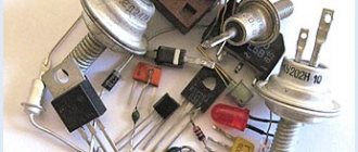
Electric current in semiconductors
Semiconductors occupy an intermediate position in electrical conductivity (or resistivity) between conductors and dielectrics. However, this division of all substances according to their property of electrical conductivity is conditional, since under the influence of a number of reasons (impurities, irradiation, heating), the electrical conductivity and resistivity of many substances change quite significantly, especially in semiconductors.
In this regard, semiconductors are distinguished from metals by a number of characteristics:
1. The resistivity of semiconductors under normal conditions is much greater than that of metals;
2. The resistivity of pure semiconductors decreases with increasing temperature (for metals it increases);
3. when semiconductors are illuminated, their resistance decreases significantly (light has almost no effect on the resistance of metals):
4. A tiny amount of impurities has a strong effect on the resistance of semiconductors.
Semiconductors include 12 chemical elements in the middle part of the periodic table (Fig. 1) - B, C, Si, P, S, Ge, As, Se, Sn, Sb, Te, I, compounds of elements of the third group with elements of the fifth group, many metal oxides and sulfides, a number of other chemical compounds, some organic substances. Germanium Ge and silicon Si have the greatest application in science and technology.
Rice. 1
Semiconductors can be pure or with impurities. Accordingly, a distinction is made between intrinsic and impurity conductivity of semiconductors. Impurities, in turn, are divided into donor and acceptor.
General concepts.
Why semiconductor
diode, transistor or thyristor?
Because the basis of these radio components are semiconductors
- substances that can both conduct electric current and prevent its passage.
This is a large group of substances used in radio engineering (germanium, silicon, selenium, copper oxide), but mainly only Silicon
(Si) and
Germanium
(Ge).
In terms of their electrical properties, semiconductors occupy a middle place between conductors and non-conductors of electric current.
Intrinsic electrical conductivity
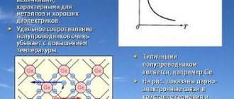
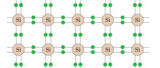
To understand the mechanism of electrical conductivity in semiconductors, let us consider the structure of semiconductor crystals and the nature of the bonds that hold the atoms of the crystal near each other. Crystals of germanium and other semiconductors have an atomic crystal lattice (Fig. 2).
Rice. 2
A planar diagram of the structure of germanium is shown in Figure 3.
Rice. 3
Germanium is a tetravalent element; in the outer shell of the atom there are four electrons that are weaker bound to the nucleus than the rest. The number of nearest neighbors of each germanium atom is also 4. The four valence electrons of each germanium atom are bonded to the same electrons of neighboring atoms by chemical pair electrons ( covalent
) connections. In the formation of this bond, one valence electron from each atom participates, which are split off from the atoms (collectivized by the crystal) and, during their movement, spend most of the time in the space between neighboring atoms. Their negative charge holds the positive germanium ions near each other. This kind of connection can be conventionally depicted by two lines connecting the nuclei (see Fig. 3).
But the itinerant pair of electrons does not belong only to two atoms. Each atom forms four bonds with its neighbors, and a given valence electron can move along any of them (Fig. 4). Having reached a neighboring atom, it can move on to the next one, and then further along the entire crystal. The collectivized valence electrons belong to the entire crystal.
Rice. 4
Covalent bonds of germanium are quite strong and do not break at low temperatures. Therefore, germanium does not conduct electric current at low temperatures. The valence electrons involved in the bonding of atoms are firmly attached to the crystal lattice, and the external electric field does not have a noticeable effect on their movement. The silicon crystal has a similar structure.
Electrical conductivity of a chemically pure semiconductor is possible when the covalent bonds in the crystals are broken and free electrons appear.
The additional energy that must be expended to break a covalent bond and make an electron free is called activation energy
.
Electrons can obtain this energy by heating the crystal, by irradiating it with high-frequency electromagnetic waves, etc.
As soon as an electron, having acquired the necessary energy, leaves a localized bond, a vacancy is formed on it. This vacancy can easily be filled by an electron from a neighboring bond, which thus also creates a vacancy. Thus, due to the movement of bonding electrons, vacancies move throughout the crystal. This vacancy behaves in exactly the same way as a free electron - it moves freely throughout the volume of the semiconductor. Moreover, taking into account that both the semiconductor as a whole and each of its atoms are electrically neutral with intact covalent bonds, we can say that the departure of an electron from a bond and the formation of a vacancy is actually equivalent to the appearance of an excess positive charge on this bond. Therefore, the resulting vacancy can be formally considered as a positive charge carrier, which is called a hole
(Fig. 5).
Rice. 5
Thus, the departure of an electron from a localized bond generates a pair of free charge carriers—an electron and a hole. Their concentration in a pure semiconductor is the same. At room temperature, the concentration of free carriers in pure semiconductors is low, approximately 109 ÷ 1010 times less than the concentration of atoms, but it increases rapidly with increasing temperature.
- Compare with metals: there the concentration of free electrons is approximately equal to the concentration of atoms.
In the absence of an external electric field, these free electrons and holes move chaotically in the semiconductor crystal.
In an external electric field, electrons move in the direction opposite to the direction of the electric field strength. Positive holes move in the direction of the electric field strength (Fig. 6). The process of moving electrons and holes in an external field occurs throughout the entire volume of the semiconductor.
Rice. 6
The total electrical conductivity of a semiconductor consists of hole and electron conductivities. Moreover, in pure semiconductors the number of conduction electrons is always equal to the number of holes. Therefore, they say that pure semiconductors have electron-hole conductivity
, or
self-conductivity
.
With increasing temperature, the number of breaks of covalent bonds increases and the number of free electrons and holes in crystals of pure semiconductors increases, and, consequently, the electrical conductivity increases and the resistivity of pure semiconductors decreases. A graph of the resistivity of a pure semiconductor versus temperature is shown in Fig. 7.
Rice. 7
In addition to heating, the breaking of covalent bonds and, as a consequence, the emergence of intrinsic conductivity of semiconductors and a decrease in resistivity can be caused by illumination (photoconductivity of a semiconductor), as well as by the action of strong electric fields.
Impurity conductivity of semiconductors
The conductivity of semiconductors increases with the introduction of impurities, when, along with their own conductivity, additional impurity conductivity appears.
Impurity conductivity
semiconductors is called conductivity due to the presence of impurities in the semiconductor.
Impurity centers can be:
1. atoms or ions of chemical elements embedded in a semiconductor lattice;
2. excess atoms or ions embedded in the interstices of the lattice;
3. various other defects and distortions in the crystal lattice: empty nodes, cracks, shifts that occur during deformation of crystals, etc.
By changing the concentration of impurities, you can significantly increase the number of charge carriers of one sign or another and create semiconductors with a predominant concentration of either negatively or positively charged carriers.
Impurities can be divided into donor (giving away) and acceptor (receiving) impurities.
Donor impurity
- From the Latin “donare” - to give, to sacrifice.
Let us consider the mechanism of electrical conductivity of a semiconductor with a donor pentavalent arsenic impurity As, which is introduced into a crystal, for example, silicon. The pentavalent arsenic atom donates four valence electrons to form covalent bonds, and the fifth electron is unoccupied in these bonds (Fig. 8).
Rice. 8
The abstraction energy (ionization energy) of the fifth valence electron of arsenic in silicon is 0.05 eV = 0.08⋅10-19 J, which is 20 times less than the energy of electron abstraction from a silicon atom. Therefore, already at room temperature, almost all arsenic atoms lose one of their electrons and become positive ions. Positive arsenic ions cannot capture electrons from neighboring atoms, since all four bonds are already equipped with electrons. In this case, there is no movement of the electron vacancy—the “hole”—and the hole conductivity is very small, i.e. practically absent.
Donor impurities
- these are impurities that easily give up electrons and, therefore, increase the number of free electrons. In the presence of an electric field, free electrons come into ordered motion in a semiconductor crystal, and electronic impurity conductivity appears in it. The result is a semiconductor with predominantly electronic conductivity, called an n-type semiconductor. (From Latin negativus - negative).
Since in an n-type semiconductor the number of electrons is much greater than the number of holes, electrons are the majority charge carriers, and holes are minority carriers.
Acceptor impurity
- From the Latin “acceptor” - receiver.
In the case of an acceptor impurity, for example, trivalent indium In, the impurity atom can give its three electrons to carry out a covalent bond with only three neighboring silicon atoms, and one electron is “missing” (Fig. 9). One of the electrons of neighboring silicon atoms can fill this bond, then the In atom will become a stationary negative ion, and a hole will form in the place of the electron that left one of the silicon atoms. Acceptor impurities, capturing electrons and thereby creating mobile holes, do not increase the number of conduction electrons. The majority charge carriers in a semiconductor with an acceptor impurity are holes, and the minority charge carriers are electrons.
Rice. 9
Acceptor impurities
- These are impurities that provide hole conductivity.
Semiconductors in which the concentration of holes exceeds the concentration of conduction electrons are called p-type semiconductors (From the Latin positivus - positive.).
It should be noted that the introduction of impurities into semiconductors, as in any metals, disrupts the structure of the crystal lattice and impedes the movement of electrons. However, the resistance does not increase due to the fact that increasing the concentration of charge carriers significantly reduces the resistance. Thus, the introduction of a boron impurity in an amount of 1 atom per hundred thousand silicon atoms reduces the electrical resistivity of silicon by approximately a thousand times, and an admixture of one indium atom per 108 - 109 germanium atoms reduces the electrical resistivity of germanium by millions of times.
If both donor and acceptor impurities are simultaneously introduced into a semiconductor, then the nature of the semiconductor’s conductivity (n- or p-type) is determined by the impurity with a higher concentration of charge carriers.
Hole
This term has other meanings, see Hole (meanings).
| It is necessary to check the quality of the translation and bring the article into compliance with the stylistic rules of Wikipedia. You can help improve this article by correcting errors. Original in English - Electron hole. This mark has been on the article since May 1, 2012. |
| Hole | |
| Symbol: | h (English hole) |
| |
| Compound: | Quasiparticle |
| Classification: | Light holes, heavy holes |
| Named after whom and/or what: | Lack of electron |
| Quantum numbers: | |
| Electric charge: | +1 |
| Spin: | Determined by the spin of electrons in the valence band ħ |
A hole is a quasiparticle, a carrier of a positive charge equal to the elementary charge in semiconductors.
Definition according to GOST 22622-77: “An unfilled valence bond, which manifests itself as a positive charge, numerically equal to the charge of an electron.”
The concept of a hole is introduced in band theory to describe electronic phenomena in the valence band, which is not completely filled with electrons. In the electronic spectrum of the valence band, several zones often appear that differ in effective mass and energy position (zones of light and heavy holes, zone of spin-orbit split holes).
Electron-hole transition
An electron-hole junction (abbreviated p-n junction) occurs in a semiconductor crystal that simultaneously has regions with n-type (contains donor impurities) and p-type (with acceptor impurities) conductivities at the boundary between these regions.
Let's say we have a crystal in which there is a semiconductor region with hole (p-type) conductivity on the left, and with electronic (n-type) conductivity on the right (Fig. 10). Due to thermal motion, when a contact is formed, electrons from the n-type semiconductor will diffuse into the p-type region. In this case, an uncompensated positive donor ion will remain in the n-type region. Having passed into the region with hole conductivity, the electron very quickly recombines with the hole, and an uncompensated acceptor ion is formed in the p-type region.
Rice. 10
Similar to electrons, holes from the p-type region diffuse into the electron region, leaving an uncompensated negatively charged acceptor ion in the hole region. Having passed into the electronic region, the hole recombines with an electron. As a result, an uncompensated positive donor ion is formed in the electronic region.
As a result of diffusion, a double electric layer of oppositely charged ions is formed at the boundary between these regions, thickness l
which does not exceed fractions of a micrometer.
An electric field with intensity Ei
. The electric field of an electron-hole junction (pn junction) prevents electrons and holes from moving further across the interface between the two semiconductors. The blocking layer has increased resistance compared to other volumes of semiconductors.
External electric field with intensity E
affects the resistance of the blocking electric field. If the n-semiconductor is connected to the negative pole of the source, and the plus of the source is connected to the p-semiconductor, then under the influence of the electric field, electrons in the n-semiconductor and holes in the p-semiconductor will move towards each other towards the interface of the semiconductors (Fig. 11). Electrons, crossing the border, “fill” holes. With such a forward direction of the external electric field, the thickness of the blocking layer and its resistance continuously decrease. In this direction, electric current passes through the pn junction.
Rice. eleven
The considered direction of the pn junction is called direct
.
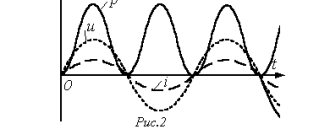
The dependence of current on voltage, i.e. The current-voltage characteristic
of the direct junction is shown in Fig. 12 with a solid line.
Rice. 12
If the n-semiconductor is connected to the positive pole of the source, and the p-semiconductor to the negative, then electrons in the n-semiconductor and holes in the p-semiconductor under the influence of the electric field will move from the interface in opposite directions (Fig. 13). This leads to a thickening of the barrier layer and an increase in its resistance. The direction of the external electric field that expands the blocking layer is called blocking
(
reverse
). With this direction of the external field, the electric current of the main charge carriers does not pass through the contact of two p- and p-semiconductors.
Rice. 13
The current through the pn junction is now due to the electrons present in the p-type semiconductor and the holes from the n-type semiconductor. But there are very few minority charge carriers, so the conductivity of the junction turns out to be insignificant, and its resistance is large. The considered direction of the pn junction is called reverse
, its current-voltage characteristic is shown in Fig. 12 dashed line.
Please note that the scale of current measurement for forward and reverse transitions differs by a thousand times.
Note that at a certain voltage applied in the opposite direction, breakdown
(i.e. destruction) of the pn junction.
Solid state physics
In solid state physics, a hole is the absence of an electron in an almost completely filled valence band. In some ways, the behavior of a hole in a semiconductor is similar to the behavior of a bubble in a full water bottle.
Hole conduction can be explained using the following analogy: There are a number of people sitting in an auditorium where there are no spare chairs. If someone from the middle of the row wants to leave, he climbs over the back of the chair into the empty row and leaves. Here the empty row is an analogue of the conduction band, and the departed person can be compared to a free electron. Let's imagine that someone else comes and wants to sit down. It’s hard to see from the empty row, so he doesn’t sit there. Instead, the person sitting near the empty chair moves to it, and all his neighbors repeat this after him. Thus, the empty space seems to move to the edge of the row. When this place is near the new viewer, he can sit down.
In this process, each person sitting moved along the row. If the spectators had a negative charge, such movement would be electrical conduction. If, in addition, the chairs are positively charged, then only the free seat will have a non-zero total charge. This is a simple model showing how hole conduction works. However, in fact, due to the properties of the crystal lattice, the hole is not in a specific place, as described above, but is spread out over an area measuring many hundreds of unit cells.
To create holes in semiconductors, crystals are doped with acceptor impurities. In addition, holes can also appear as a result of external influences: thermal excitation of electrons from the valence band to the conduction band, illumination with light, or irradiation with ionizing radiation.
In the case of Coulomb interaction of a hole with an electron from the conduction band, a bound state called an exciton is formed.
Heavy holes are the name of one of the branches of the energy spectrum of the valence band of a crystal.
Semiconductor devices
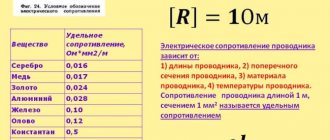
Thermistors
The electrical resistance of semiconductors is highly dependent on temperature. This property is used to measure temperature by current strength in a circuit with a semiconductor. Such devices are called thermistors
or
thermistors
. The semiconductor substance is placed in a metal protective case, which contains insulated leads for connecting the thermistor to the electrical circuit.
Changing the resistance of thermistors when heating or cooling allows them to be used in instruments for measuring temperature, to maintain a constant temperature in automatic devices - in closed thermostat chambers, to provide fire alarms, etc. There are thermistors for measuring both very high ( T
≈ 1300 K) and very low (
T
≈ 4 - 80 K) temperatures.
A schematic representation (Fig. a) and photograph (Fig. b) of the thermistor is shown in Figure 14.
- A
- b
Rice. 14
Photoresistors
The electrical conductivity of semiconductors increases not only when heated, but also when illuminated. Electrical conductivity increases due to the breaking of bonds and the formation of free electrons and holes due to the energy of light incident on the semiconductor.
Devices that take into account the dependence of the electrical conductivity of semiconductors on lighting are called photoresistors
.
The materials for the manufacture of photoresistors are compounds such as CdS, CdSe, PbS and a number of others.
The miniature size and high sensitivity of photoresistors allow them to be used for recording and measuring weak light fluxes. Photoresistors are used to determine the quality of surfaces, control the dimensions of products, etc.
A schematic representation (Fig. a) and photograph (Fig. b) of the photoresistor is shown in Figure 15.
- A
- b
Rice. 15
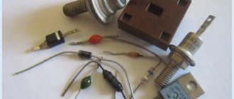
Semiconductor diode
The ability of a pn junction to allow current to flow in one direction is used in semiconductor devices called diodes
.
Semiconductor diodes are made from germanium, silicon, selenium and other substances.
To prevent harmful effects of air and light, the germanium crystal is placed in a sealed metal case. Semiconductor diodes are the main elements of AC rectifiers (more precisely, they serve to convert alternating current into a pulsating direct current.)
A schematic representation (Fig. a) and photograph (Fig. b) of a semiconductor diode is shown in Figure 16.
- A
- b
Rice. 16
LEDs
Light-emitting diode
or
light-emitting diode
- a semiconductor device with a pn junction that creates optical radiation when an electric current is passed through it.
The emitted light lies in a narrow range of the spectrum; its spectral characteristics depend, among other things, on the chemical composition of the semiconductors used in it.
Applications of LEDs
: in lighting, as indicators (power indicator on the instrument panel, alphanumeric display), as a light source in lanterns and traffic lights, as sources of optical radiation (remote controls, light telephones), in the backlight of LCD screens (mobile phones, monitors , TVs), etc.
A schematic representation (Fig. a) and photograph (Fig. b) of the LED is shown in Figure 17.
- A
- b
Rice. 17
See also
- Wikipedia: Diode
- Wikipedia: LEDs
- Wikipedia: Thermistor
- Wikipedia: Photoresistor
Production
Research and the first attempts to create semiconductor devices were carried out in the USSR back in the 1920-30s. In 1924, at the Nizhny Novgorod Radio Laboratory, scientist O. V. Losev created a semiconductor detector-amplifier and detector-generator of electromagnetic radiation at frequencies up to tens of MHz. On this basis, for the first time in the world, a detector transceiver device was created - cristadine.
Later, research institutes and centers were created in the USSR to develop the industry. In 1956, the Semiconductor Devices Plant was put into operation. Among the plant's products at that time were finger lamps for wide use and subminiature rod lamps, the first semiconductor diodes D2, diodes D9, D10, D101-103A, D11, zener diodes D808-813.
In 2014, a new production line was launched at the Semiconductor Devices Plant for the development and development of modern complex packages for integrated circuits.
Among the major manufacturers of integrated circuits in the USSR and the Russian Federation is OKB Iskra. The company's products include high-current transistors, transistor modules and power fast-recovery diodes. Currently, the company produces microcircuits for the needs of the Russian navy, army, space and nuclear energy.
At the moment, both enterprises are part of the Ruselectronics holding.
> See also
- Semiconductor
- Semiconductor materials
Literature
- Aksenovich L. A. Physics in secondary school: Theory. Tasks. Tests: Textbook. allowance for institutions providing general education. environment, education / L. A. Aksenovich, N. N. Rakina, K. S. Farino; Ed. K. S. Farino. - Mn.: Adukatsiya i vyakhavanne, 2004. - P. 300-308.
- Burov L.I., Strelchenya V.M. Physics from A to Z: for students, applicants, tutors. - Mn.: Paradox, 2000. - P. 219-228.
- Myakishev G. Ya. Physics: Electrodynamics. 10 – 11 grades: textbook for in-depth study of physics / G.Ya. Myakishev, A.Z. Sinyakov, B.A. Slobodskov. - M.: Bustard, 2005. - P. 309-320.
- Yavorsky B. M., Seleznev Yu. A. A reference guide to physics for those entering universities and self-education. - M.: Nauka, 1984. - P. 165-169.