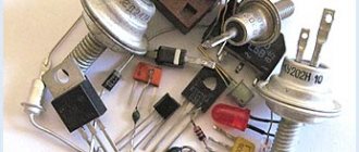
Hello dear readers of the site. The site has a section dedicated to beginner radio amateurs, but so far I haven’t really written anything for beginners taking their first steps into the world of electronics. I fill this gap, and with this article we begin to get acquainted with the structure and operation of radio components (radio components).
Let's start with semiconductor devices. But to understand how a diode, thyristor or transistor works, you need to understand what a semiconductor . Therefore, we will first study the structure and properties of semiconductors at the molecular level, and then we will deal with the operation and design of semiconductor radio components.
General concepts.
Why semiconductor
diode, transistor or thyristor?
Because the basis of these radio components are semiconductors
- substances that can both conduct electric current and prevent its passage.
This is a large group of substances used in radio engineering (germanium, silicon, selenium, copper oxide), but mainly only Silicon
(Si) and
Germanium
(Ge).
In terms of their electrical properties, semiconductors occupy a middle place between conductors and non-conductors of electric current.
Properties of semiconductors.
The electrical conductivity of conductors is highly dependent on the ambient temperature. At very low
At temperatures close to absolute zero (-273°C), semiconductors
do not conduct
electric current, and with
increasing
temperature, their resistance to current
decreases
.
If you shine light
, then its electrical conductivity begins to increase.
photovoltaic
were created .
Semiconductors are also capable of converting light energy into electric current, for example, solar panels. And when impurities
of certain substances are introduced into semiconductors, their electrical conductivity increases sharply.
Structure of semiconductor atoms.
Germanium and silicon are the main materials of many semiconductor devices and have four valence electrons
.
germanium atom
consists of 32 electrons, and the
silicon
of 14. But only
28
electrons of the germanium atom and
10
electrons of the silicon atom, located in the inner layers of their shells, are firmly held by the nuclei and never come off from them.
Only four
valence electrons of the atoms of these conductors can become free, and even then not always.
And if a semiconductor atom loses at least one electron, then it becomes a positive ion
.
In a semiconductor, the atoms are arranged in a strict order: each atom is surrounded by four
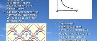
the same atoms. Moreover, they are located so close to each other that their valence electrons form single orbits passing around neighboring atoms, thereby linking the atoms into a single whole substance.
Let us imagine the relationship of atoms in a semiconductor crystal in the form of a flat diagram. In the diagram, red balls with a plus symbol, conventionally, indicate atomic nuclei
(positive ions), and the blue balls are
valence electrons
.
Here you can see that around each atom there are four
exactly the same atoms, and each of these four has a connection with four other atoms, etc.
Each atom is bound to each neighboring atom by two
valence electrons, with one electron being its own and the other borrowed from the neighboring atom.
Such a bond is called two-electron or covalent
.
In turn, the outer layer of the electron shell of each atom contains eight
electrons:
four
of their own, and
one each
borrowed from four
neighboring
atoms.
Here you can no longer distinguish which of the valence electrons in the atom is “yours” and which is “foreign”, since they have become common. With such a connection of atoms in the entire mass of a germanium or silicon crystal, we can consider that the semiconductor crystal is one large molecule
. In the figure, pink and yellow circles show the connection between the outer layers of the shells of two neighboring atoms.
Symmetrical current-voltage characteristic
When the polarity of the voltage changes, the current in the semiconductor begins to flow in the opposite direction. And it changes according to the same law. This suggests that the semiconductor element has a symmetrical current-voltage characteristic. If one part of the element is of the hole type, and the second is of the electronic type, then a pn junction (electron-hole) appears at the boundary of their contact. It is precisely these transitions that are present in all elements - transistors, diodes, microcircuits. But only in microcircuits several transistors are assembled on one chip at once - sometimes there are more than a dozen of them.
Electrical conductivity of a semiconductor.
Consider a simplified drawing of a semiconductor crystal, where atoms are represented by a red ball with a plus, and interatomic bonds are shown by two lines symbolizing valence electrons.
At temperatures close to absolute zero, a semiconductor does not conduct
current, since there are no
free electrons
.
But with increasing temperature, the connection of valence electrons with atomic nuclei weakens
and some of the electrons, due to thermal movement, can leave their atoms.
An electron released from an interatomic bond becomes “ free
”, and where it was before, an empty space is formed, which is conventionally called
a hole
.
The higher
temperature of the semiconductor, the
more
free electrons and holes it becomes.
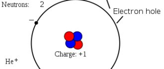
As a result, it turns out that the formation of a “hole” is associated with the departure of a valence electron from the shell of an atom, and the hole itself becomes a positive
electric charge equal to
the negative
charge of the electron.
Now let's look at the figure, which schematically shows the phenomenon of current generation in a semiconductor
.
If you apply some voltage to the semiconductor, the “+” and “-” contacts, then a current will arise in it. Due to thermal phenomena
, in a semiconductor crystal, a certain number of electrons will begin
to be released
(blue balls with arrows).
Electrons, attracted by the positive
pole of the voltage source, will
move
towards it, leaving behind
holes
that will be filled with other
released electrons
.
That is, under the influence of an external electric field, charge carriers acquire a certain speed of directional movement and thereby create an electric current
.
For example: the released electron closest to the positive pole of the voltage source is attracted
this pole.
By breaking an interatomic bond and leaving it, an electron leaves
behind
a hole
.
Another released electron, which is located at some distance
from the positive pole, is also
attracted
by the pole and
moves
towards it, but
when it encounters
a hole on its way, it is attracted into it
by the nucleus
of the atom, restoring the interatomic bond.
The resulting new
the hole after the second electron
is filled by
the third released electron located next to this hole (Figure No. 1).
In turn, the holes
located closest to
the negative
pole are filled with other
released electrons
(Figure No. 2). Thus, an electric current arises in the semiconductor.
While there is an electric field
, this process
is continuous
: interatomic bonds are broken - free electrons appear - holes are formed. The holes are filled with released electrons - interatomic bonds are restored, while other interatomic bonds are broken, from which electrons leave and fill the next holes (Figure No. 2-4).
From this we conclude: electrons move from the negative pole of the voltage source to the positive, and holes move from the positive pole to the negative
.
p - n Transition .
A pn junction is the simplest semiconductor structure that is used in most semiconductor devices. To obtain a pn junction, a semiconductor sample is doped (impurities are introduced into it) in such a way that donor impurities predominate in one part and acceptor impurities in the other, resulting in contact between an n-type semiconductor and a p-type semiconductor.
The main property of a pn junction is its ability to pass current in only one direction if a voltage is applied to the sample so that the conduction is carried out by the main current carriers, as shown in the figure above: “-” on the side of the n-type semiconductor, “+” - from the p-type side (electrons from the n-region move to the p-region, and vice versa).
If we now change the polarity of the applied voltage U, then practically no current flows through the pn junction, since the transition through the contact is carried out by minority carriers, of which there are few. The current-voltage characteristic of the p-n junction is shown in the figure below.
Electron-hole conductivity.
In a “pure” semiconductor crystal, the number of released
at a given moment, electrons are equal to the number of
formed
in this case, therefore the electrical conductivity of such a semiconductor
is small
, since it provides
great
resistance to the electric current, and such electrical conductivity is called
intrinsic
.
But if you add it to a semiconductor as an impurity
a certain number of atoms of other elements, then its electrical conductivity will increase several times, and depending on
the structure
of the atoms of impurity elements, the electrical conductivity of the semiconductor will be
electronic
or
hole
.
Electronic conductivity.
Let's say that in a semiconductor crystal in which the atoms have four valence electrons, we replace one atom with an atom that has five
valence electrons.
This atom with its four
electrons will bond with four neighboring atoms of the semiconductor, and
the fifth
valence electron will remain “
extra
” - that is, free.
And the more
such atoms there are in the crystal, the
more
free electrons there will be, which means that such a semiconductor in its properties will approach the metal, and in order for an electric current to pass through it,
interatomic bonds in it do not necessarily have to be destroyed
.
n” type semiconductors
", or
n
-type semiconductors.
Here the Latin letter n comes from the word “negative” - that is, “negative”. It follows that in an n
-type
the main
charge carriers are
electrons
, and not the main ones are holes.
Energy gap
The valence orbitals of atoms in a crystal lattice are divided into two groups of energy levels - the free band, located at the highest level and determining the electrical conductivity of semiconductors, and the valence band, located below. These levels, depending on the symmetry of the crystal lattice and the composition of the atoms, can intersect or be located at a distance from each other. In the latter case, an energy gap or, in other words, a forbidden zone appears between the zones.
The location and filling of the levels determines the electrical conductivity properties of the substance. Based on this criterion, substances are divided into conductors, insulators and semiconductors. The band gap of the semiconductor varies in the range of 0.01–3 eV, and the energy gap of the dielectric exceeds 3 eV. Metals do not have energy gaps due to the overlap of levels.
Semiconductors and dielectrics, as opposed to metals, have a valence band filled with electrons, and the nearest free band, or conduction band, is fenced off from the valence band by an energy gap - a region of forbidden electron energies.
In dielectrics, thermal energy or a small electric field is not enough to make a jump through this gap; electrons do not enter the conduction band. They are not able to move along the crystal lattice and become carriers of electric current.
To initiate electrical conductivity, an electron at the valence level must be given energy that would be sufficient to overcome the energy gap. Only by absorbing an amount of energy no less than the size of the energy gap will the electron move from the valence level to the conduction level.
If the width of the energy gap exceeds 4 eV, excitation of the conductivity of the semiconductor by irradiation or heating is practically impossible - the excitation energy of electrons at the melting temperature is insufficient to jump through the energy gap zone. When heated, the crystal will melt until electronic conduction occurs. Such substances include quartz (dE = 5.2 eV), diamond (dE = 5.1 eV), and many salts.


