The crystal oscillator is an important electronic component that provides very accurate clock frequency generation at a fraction of the cost.
Due to the piezoelectric effect, its electrical properties change during vibration. Because it is possible to make a crystal that vibrates at a specific frequency, crystal oscillators are very useful for a variety of applications. They appeared in the 1920s, and at first provided precise wave generation for radio stations. In 1970, a revolution in wristwatches occurred when they began to use high-precision quartz oscillators. Computers from the ENIAC of the 1940s to the present day use crystal oscillators to generate clock frequencies. Modern PCs still use crystal oscillators, but more sophisticated technologies are used to achieve multi-gigahertz clock speeds. The PC uses a crystal with a frequency much lower than the operating frequency and multiplies it using phase-locked loop. Computers often use a 14318 crystal because that frequency was used in older televisions and such crystals were inexpensive and widely available. In order for the crystal to vibrate, its circuitry requires additional components. In the 1970s, modular crystal oscillators gained popularity - these compact and easy-to-use microassemblies combined the crystal itself, ICs and discrete components. I became interested in how one of these modules worked, so I opened one of them and reverse engineered its chip. In this post I'll explain how it works and describe the tiny CMOS circuit that controls it. It turned out that there was more interesting stuff going on inside the module than one might have expected.
Generator module
I was studying a module from a card for the IBM PC.
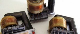
The module is housed in a rectangular metal case with 4 pins that protects the electronics from electrical noise (that's the Rasco Plus in the rectangular case on the right in the photo, not the square IC from IBM). The module generates a signal at 4.7174 MHz, as follows from the inscription on its body. Why does the card use a crystal with such an unusual frequency - 4.7174 MHz? In the 1970s, the IBM 3270 was a very popular CRT terminal. The terminals were connected by coaxial cable and used the Interface Display System Standard protocol, operating at a clock frequency of 2.3587 MHz. In the late 1980s, IBM produced interface cards to connect the IBM PC to the 3270 network. My crystal is from one of these cards (type 56X4927), and the frequency of the crystal is 4.7174 MHz - exactly twice as high as 2.3587 MHz.
The crystal oscillator module is located at the bottom right. Inscription on the case: Rasco Plus. 4.7174 MHZ, Motorola 1987. The square module on the left is an IC from IBM.
I opened the module case to look at its hybrid circuit. I expected to see a quartz crystal there, like a gemstone in a box, but I discovered that quartz oscillators use a very thin quartz disk. I damaged it when opening it, so it's missing a piece at the top right. It is visible on the left side of the photo - metal electrodes approach it on both sides. These, in turn, are connected to small pins on which the crystal is raised above the surface of the housing so that it can vibrate freely.
Inside the crystal oscillator housing are components mounted on a ceramic substrate. They are connected to the circuit with tiny gold bonding wire. A 3 nF capacitor and a 10 ohm film resistor, located on the substrate using a surface mount method, filter out noise coming from the power pin.
Quartz resonator
What is a quartz resonator?
Currently, many types of crystalline substances have been identified, but quartz minerals are most used in electronics, since in addition to being piezoelectric, it also has good mechanical strength.
Resonator - (from the Latin resono - I sound in response, I respond) - is a system that is capable of oscillating with maximum amplitude, that is, resonating, when exposed to an external force of a certain frequency and shape. It turns out that a quartz resonator in electronics, or popularly simply “quartz,” is a radio element that is capable of resonating if an alternating current of a certain frequency and shape is applied to it.
Quartz resonators look something like this.
types of quartz resonators
Quartz is a dielectric. What happens if a thin dielectric is placed between two metal plates? You'll get a capacitor! The capacitor turns out to have a very small capacity, so it is unlikely that it will be possible to measure its capacity. But they didn’t bother with the circuit designation of quartz, and on the diagrams it is shown as a rectangular piece of crystal enclosed between two capacitor plates.
designation on the diagram of a quartz resonator
Having disassembled the quartz resonator, we can see with our own eyes the quartz crystal itself. Let's open the Soviet-made quartz in a case like this.
Here we see a transparent quartz crystal placed between two metal plates, to which the leads are soldered.
what's inside a quartz resonator
In small quartzes like these
quartz resonator
thin rectangular quartz plates are used. The physical size and thickness of the quartz plate inside the quartz resonator must be strictly observed, since it is its overall dimensions that affect the main oscillation frequency. The rule here is: the thicker the plate, the lower the operating frequency of the quartz. Therefore, the highest frequencies at which quartz is made is no more than 50 MHz, since the plate is very thin, which creates difficulties in its manufacture. Yes, and you need to somehow keep it in the case without breaking it. In theory, you can squeeze the frequency out of quartz up to 200 MHz, but such quartz will work on an overtone.
Overtones of a quartz resonator
Overtones, or as they are also called, modes or harmonics, are multiple frequencies above the fundamental frequency of quartz. Using filters, the fundamental frequency of quartz is suppressed and the overtone is isolated. odd overtones are used in the overtone mode . If the fundamental frequency of quartz F is the first overtone, then its working overtones will be like 3F, 5F, 7F, 9F. It is also worth noting that the amplitude of the overtone decreases with increasing its frequency, therefore, there is no point in taking the 9th overtone, since isolating the amplitude of a small signal is very problematic.
Example: let's take quartz with a frequency of 10 Megahertz. Then we can excite it at overtones of 30 Megahertz (third overtone), 50 Megahertz (fifth overtone), 70 Megahertz (seventh overtone) and a maximum of 90 Megahertz (ninth overtone).
To somehow understand what overtones are, for example, listen to the fundamental frequency of 110 Hertz and its overtones.
The circuit that excites quartz on overtones is complex and not very reliable, since, firstly, it is necessary to “press” the main frequency of the quartz and release the overtone, and secondly, the quartz can be excited in the mode of random oscillations. In practice, they still make circuits that multiply the main frequency of quartz, which is much simpler and more reliable. There is also one more rule here: if the frequency is marked in whole numbers in Kilohertz, this is work on the fundamental harmonic, and if in Megahertz separated by commas, this is an overtone harmonic. For example: RG-05-18000 kHz is a resonator for operating at the fundamental frequency, and RG-05-27.465 MHz is for operating at the 3rd overtone.
Series and parallel quartz resonance
There are a lot of myths circulating on the Internet specifically about the quartz resonator. The most popular myth goes like this: if you apply a constant voltage to a quartz resonator, it will produce an alternating voltage with the frequency indicated on it. I might agree about the “frequency indicated on it,” but alas, about the constant voltage. The quartz crystal will simply shrink or unclench). Some people still think that quartz itself produces alternating current). Yeah, just a perpetual motion machine).
In order to understand the principle of operation of a quartz resonator, it is necessary to consider its equivalent circuit:
equivalent circuit of a quartz resonator
C is the actual capacitance between the plates of the capacitor. That is, if you remove the quartz crystal, you will be left with two plates and their leads. They are the ones who have this capacity.
C1 is the equivalent capacitance of the crystal itself. Its value is several femtoFarads. Femto is 10-15!
L1 is the equivalent inductance of the crystal.
R1 - dynamic resistance, when working with quartz it can reach from several Ohms to several KOhms
It can be noted that C1, L1 and R1 form a series oscillatory circuit, which has its own resonant frequency.
series oscillating circuit
The resonant frequency of such a circuit is calculated by the formula
formula for series resonance of a quartz resonator
But everything would be fine, but as you can see, in the equivalent circuit of a quartz resonator there is also one heavy capacitor C, which spoils the whole raspberry.
This whole circuit turns into a complex parallel oscillatory circuit. The resonant frequency of such a circuit will already be determined by the formula
formula for parallel resonance of a quartz resonator
Therefore, remember: each quartz resonator can be excited at two resonant frequencies . At the series resonance and at the parallel resonance . If we see an inscription like this on quartz
quartz frequency
this tells us that the series resonance frequency for this crystal oscillator is 8 MHz. Quartz resonators in electronics operate precisely at the frequency of series resonance. In my practice, I don’t remember anyone exciting quartz to operate at a parallel resonance frequency.
Clock quartz resonator
Most often, watch quartz looks like this.
“What kind of watch quartz is this?” - you ask. Hour quartz is a quartz with a frequency of 32,768 Hertz. Why does it have such a strange frequency? The thing is that 32,768 is 215. This quartz works in tandem with a 15-bit counter chip. This is our K176IE5 microcircuit.
The operating principle of this microcircuit is as follows: after it counts 32,768 pulses, it emits a pulse on one of the legs. This pulse on a leg with a quartz resonator at 32,768 Hertz appears exactly once per second . And as you remember, oscillation once per second is 1 Hertz. That is, on this leg the pulse will be issued with a frequency of 1 Hz. And if this is so, then why not use it in watches? This is where the name came from - watch quartz .
Currently, in wristwatches and other mobile gadgets, this counter and quartz resonator are built into one chip and provide not only counting of seconds, but also a number of other functions, such as alarm clock, calendar, etc. Such microcircuits are called RTC (Real Time C lock ) or translated from bourgeois Real Time Clock .
IC operation diagram
The photo below shows a tiny IC crystal under a microscope. Contact pads and main functional blocks are marked. The green-brown areas are the silicon that forms the IC. A yellowish metallic layer connects the components to the IC. Beneath the metal is a reddish layer of polysilicon where transistors are formed - but it is almost completely covered by the metal layer. Along the edges of the chip there is a welding wire connected to the contact pads connecting the chip to the rest of the module. Two pads (select and disable) are not connected. The chip was manufactured by Motorola in 1986. I did not find any information on the article number SC380003.
IC crystal with markings of main blocks. "FF" stands for triggers. “sel” – contact pads. “cap” – pads connected to internal capacitors
.
IS has two tasks. First, its analog components cause the crystal to vibrate. Second, its digital components divide the frequency by 1, 2, 4, or 8, and produce a high-current clock signal (the divider is set by two selector pins on the IC).
The quartz oscillator is implemented according to the circuit below, which is called the “Colpitts oscillator”. It is more complex than a conventional crystal oscillator circuit. The bottom line is that the crystal and two capacitors oscillate at a given frequency. However, the oscillations would quickly die out if not for the supporting feedback from the supporting transistor.
A typical crystal oscillator is built using a simple circuit called a “Pierce oscillator”, in which a feedback circuit is formed from a crystal and an inverter. The two grounded capacitors in the middle make it very similar to a classic Colpitts oscillator.
I'm not sure why the crystal oscillator I disassembled uses a more complex circuit that requires a tricky voltage bias.
In 1918, Edwin Colpitz, chief researcher at Western Electric, invented an inductor-capacitor crystal oscillator. Today this circuit is known as a Colpitts generator. The idea is that the inductor and capacitor form a “resonant tank” that oscillates at a frequency depending on the characteristics of the components. You can imagine that the electricity in this reservoir seems to splash back and forth between the inductor and the capacitors. The oscillations themselves would quickly die out, so an amplifier is used to feed them. In the original Colpitts oscillator, the amplifier was a vacuum tube. Later circuits switched to transistors, but this amplifier may be an operational amplifier or another type. In other circuits, the end is grounded so that there is feedback in the middle. Then the capacitors do not invert anything, so a non-inverting amplifier is used.
Simplified diagram of a Colpitts generator with basic components.
The key feature of the Colpitts generator is the two capacitors that form the voltage divider. Since they are grounded in the middle, they will have opposite voltages at the two ends: when one goes up, the other goes down. The amplifier takes the signal from one end, amplifies it, and sends it to the other. The amplifier inverts the signal, and the capacitors provide a second inversion, so that the feedback amplifies the original signal (providing a 360° phase shift).
In 1923, George Washington Pierce, a professor of physics at Harvard, replaced the inductor in the Colpitts generator with a crystal. Thanks to this, the generator became more accurate, and it began to be widely used in radio transmitters and other devices. Pierce patented his invention and made decent money from companies such as RCA and AT&T. The presence of patents led to many years of litigation, which eventually reached the Supreme Court.
For several decades, the Pierce generator was commonly called a Colpitts generator with a crystal. The Pierce generator often lacked the characteristic capacitors, instead using the stray capacitance of a vacuum tube. The terminology gradually changed, and the two different types of crystal oscillators began to be called the Colpitts oscillator (with capacitors) and the Pierce oscillator (without them).
Another change in terminology occurred due to the fact that the Colpitts oscillator, Pierce oscillator, and Clapp oscillator were topologically identical crystal oscillators, differing only in which part of the circuit was considered to be ground (collector, emitter, or base, respectively). All these oscillators can be called Colpitts oscillators, only with a common collector, common emitter or common base.
I made this excursion into history in order to show that in various sources these generators are called differently, Colpitts or Pierce generators, and in a contradictory way. The generator that I studied can be called a Colpitts generator with a common drain (by analogy with a common collector). It can also be called a Colpitts generator based on the grounding arrangement. But historically it can be called a Peirce oscillator because it uses a crystal. It is also called a single terminal crystal oscillator because only one terminal of the crystal is connected to the external circuit (the other is grounded).
Simplified generator circuit
Increasing the voltage on the crystal turns on the transistor, current flows into the capacitors, increasing the voltage across them (and on the crystal). Reducing the voltage on the crystal turns off the transistor, the current drain (circle with arrow) draws current from the capacitors, reducing the voltage on the crystal. Thus, feedback from the transistor amplifies the oscillations of the crystal, maintaining them.
Bias voltage and current circuits are an important part of this circuit. The bias voltage sets the transistor's gate somewhere between on and off, so voltage fluctuations across the chip turn it on and off. The bias current is halfway between the transistor's on and off currents, so the current flowing into and out of the capacitors is balanced (I'm simplifying by talking about on and off states - in reality the signal will be a sine wave).
Bias voltage and current circuits are moderately complex analog circuits consisting of a bunch of transistors and a few resistors. I will not describe them in detail, I will only say that they use feedback circuits to generate the required fixed values of voltage and current.
A significant part of the IC is occupied by five capacitors. In the diagram, one is located at the top, three run in parallel to form the bottom capacitor in the circuit, and one stabilizes the bias voltage circuit. The photo of the crystal below shows one of the capacitors after the top metal layer has been dissolved. The red and green areas are the polysilicon that forms the top plate of the capacitor along with the metal layer. The pinkish area located under the polysilicon is probably silicon nitride, which forms the dielectric layer. Doped silicon, which is not visible in the photo, forms the bottom plate of the capacitor.
Capacitor on chip. The large pale square on the left is the pad for connecting the bonded wire to the IC. The complex structures on the left are the clamping contact diodes. The clover-like structures on the right are transistors.
Interestingly, the capacitors on the chip are not connected together. They are connected to three platforms connected to each other by welding wire. Perhaps this gives the circuit flexibility - the circuit's capacitance can be changed by removing the conductor leading to the capacitor.
Piezoelectrics
In fact, quartz is one of the most abundant minerals in the earth's crust. Its share is about 60%! If semiconductor radio components are mainly made of silicon, then quartz also consists of silicon but combined with oxygen. Its chemical formula is SiO2.
The mineral quartz looks something like this.
mineral quartz
Well, just like some kind of treasure! But the value of this treasure is hidden not in the quartz itself, but in the properties it has. And this quartz effect has revolutionized precision electronics for generating highly stable electrical signal oscillations.
Back in the 19th century, the two Curie brothers discovered the interesting property of some solid crystals to generate emf by deforming these crystals. Deformation is a change in the shape of a body through torsion, impact, stretching, and so on. So, when they hit such crystals, they discovered that they could produce some kind of short-term voltage.
piezoelectric effect
But they also found the opposite effect. When voltage was applied to such crystals, these crystals themselves deformed. It was practically invisible to the naked eye. This effect was called the piezoelectric effect , and the substances were called piezoelectrics .
It should be noted that EMF occurs only during compression or tension. Maybe you thought that you could press such a crystal with some heavy block and receive energy from it all your life? No matter how it is! By the way, a radio element, a piezoelectric emitter, also belongs to piezoelectrics, and EMF can be obtained from it. Below you can see this case in the video. An LED soldered to the piezo emitter lights up when the piezo emitter itself is struck.
https://youtu.be/b1kGfBikKTw
Not long ago I watched a film on National Geographic. There, entire piezoelectric plates were installed on the road. People walked on them and generated electrical energy without knowing it). By the way, very free, clean and renewable energy. Okay, I got distracted... So, quartz crystals also have a piezoelectric effect and are also capable of generating EMF or deforming (bending, changing shape) under the influence of electric current.
Digital circuit
On the right side of the chip is a digital circuit that divides the crystal's output frequency by 1, 2, 4, or 8. Thanks to it, the same crystal can output four frequencies. The divider is made up of three flip-flops connected in series. Each divides the incoming pulse in half. A 4 to 1 multiplexer selects between the original pulse frequency or the output from one of the flip-flops. Selection is accomplished using wires that connect to two selection pads on the right side of the chip. The final frequency is fixed at the production stage. Four NAND gates along with inverters are used to decode the pins and generate four control signals to the multiplexer and flip-flops.
Electrical parameters
Equivalent circuit of a quartz resonator is an electrical description of a quartz resonator operating at a resonant frequency. The equivalent circuit of a quartz resonator is shown in Figure 1. C0 is the shunt capacitance. R1, L1 and C1 are dynamic resistance, dynamic inductance and dynamic capacitance, respectively. The dynamic parameters are the corresponding equivalents of the resonator as an electromechanical system and are determined mainly by the cutoff characteristics of the quartz element.
It will be interesting➡ What is a reed switch and how is it used in everyday life?
Shunt capacitance C0 – Capacitance between the terminals of the crystal. It is measured in picofarads. The shunt capacitance consists of the parasitic capacitance of the quartz, the capacitance of the crystal electrode region, and the capacitance contributed by the crystal holder. The shunt capacitance has a value of the order of units of pF. Dynamic resistance R1 – Parameter characterizing energy losses in the oscillatory circuit. The dynamic resistance R1 of quartz resonators varies in the range from several Ohms to hundreds of kOhms, depending on the resonance frequency, harmonic number and a number of design factors.
Set of quartz resonators.
Implementation of CMOS logic
The chip is built on CMOS (complementary metal-oxide-semiconductor) logic. It uses two types of transistors, N-MOS and P-MOS, working together. The diagram below shows the design of an N-MOS transistor. A transistor can be thought of as a switch between source and drain that controls a gate. The source and drain (green) consist of sections of silicon with additives that change its semiconductor properties - N+ silicon. The valve is made of a special silicon, polysilicon, separated from the silicon substrate by a very thin insulating layer of oxide layer. The N-MOS transistor turns on when the valve is pulled up.
Structure of an N-MOS transistor. The structure of the P-MOS transistor is similar, but the N- and P-type silicon sections are swapped.
The structure of a P-MOS transistor is the opposite of an N-MOS: the source and drain consist of P+ silicon embedded in N silicon. It also works opposite to the N-MOS transistor: it turns on when the valve is pulled down. Typically, P-MOS transistors pull the drain up and N-MOS transistors pull down. In CMOS, transistors work to complement each other, pulling the output signal up or down as needed.
The diagram below shows how a NAND gate is implemented in CMOS. If a 0 is applied to the input, the corresponding P-MOS transistor (top) will turn on and pull the output up. If both inputs are 1, the NMOSFET (bottom) will turn on and pull the output down. Thus, the circuit implements the NAND function.
The diagram below shows what a NAND gate looks like on a die. Unlike textbook images, real transistors have complex, curved shapes. On the left side there is a P-MOS transistor, and on the right there is an N-MOS transistor. The reddish traces above the silicon are the polysilicon that forms the gates. Most of the silicon in the substrate is conductive due to additives, and appears slightly darker than non-conducting silicon without additives on the left and right edges, as well as in the center. To make this photo, the metal layer was etched away. The yellow lines indicate where metal conductors used to be. The circles are connections between the metal layer and the underlying layers, silicon or polysilicon.
What a NAND gate looks like on a chip
The transistor in the photo can be compared with the NAND gate circuit. Look at the polysilicon formed transistor gates, and what they share. From section +5 there is a path to the output through the long P-MOS transistor on the left. The second path is through the small P-MOS transistor in the center - this shows that the transistors are connected in parallel. Each gate controls one of the inputs. On the left, the path from ground to the output should go through both concentric N-MOS transistors - they are connected in series.
This IC also uses many ring gate transistors. This unusual element arrangement technique makes it possible to place many parallel transistors at a high density. The photo below shows 16 ring gate transistors. The copper-colored clover-like patterns are the drain of the transistors, and on the outside is the source. The metal layer (here it is removed) combines all sources, valves and drains, respectively. Parallel transistors work like one big one. Parallel transistors are used to supply high currents to the output. In a bias circuit, different numbers of transistors (6, 16, or 40) are connected together to produce the desired current ratio.
14.993 and 599.720 kHz
I combined these quartzes because they have a similar design. And their release date is almost the same.
Their design is very similar to quartz in a carbolite body, but the “glass” itself is made of thin-walled finned metal (aluminum?). The meaning of this fin, by the way, eludes me - increased heat dissipation is not expected here, and it is also unlikely to serve as stiffening ribs.
| 25 - 75 MHz | Third harmonic | ||
| 75 - 100 MHz | Fifth harmonic | ||
| HC-49/US | 3 - 33.5 MHz | Fundamental harmonic | |
| 26 - 75 MHz | Third harmonic | ||
| Frequency stability | HC-49/U | ±30 x10 -6 | Tamb.=25°C |
| HC-49/US | |||
| Temperature frequency stability | HC-49/U | ±50 x10 -6 | -20. +70°C |
| HC-49/US | -10. +60°C | ||
| Operating temperature range | HC-49/U | -20. +70°C | |
| HC-49/US | -10. +60°C | ||
| Parallel capacity | HC-49/U | no more than 7 pF | |
| HC-49/US | |||
| Load capacity | HC-49/U | 20 pF (8.50 pF) | |
| HC-49/US | |||
| Aging | HC-49/U | 5×10 -6 per year | |
| HC-49/US |
| They differ in size and pin design. |
There are no markings on them that would allow identifying the manufacturer. Perhaps this is the “Factory of Precision Instruments” at the Research Institute of Precision Instruments, now it is called “Etna”. At least they definitely produced quartz in such a case. By the way, this is one of the first domestic quartz production facilities; it was created in 1943.
Transfer valve
Another key circuit of the chip is the transfer gate. It works like a switch through which the signal either passes through or does not. The diagram below shows how a transfer gate is made from two transistors, an N-MOS transistor and a P-MOS transistor. If a high voltage is applied to the enable line, both transistors turn on and the input signal passes to the output. If the voltage is low, they turn off, blocking the signal. The symbol of the transfer valve in the diagrams is shown on the right.
Low power consumption in KG
Mobile electronics and the Internet of Things (IoT) are creating great demand for low-frequency crystal oscillators, which are needed for extremely low-power circuits. For such purposes, the ECS-327MVATX chip in the SMD version (cases from 2016 to 7050) with a fixed frequency of 32.768 kHz is suitable. It consumes only 200 µA and has a CMOS output. It is ideal for use with Real Time Clock (RTC) and Internet of Things, providing frequency stability ranging from ±20 ppm to ±100 ppm over a temperature range of -40 to +85 C.
To minimize energy consumption, many generators allow shutdown. For example, the ECS-5032MV with CMOS output in a 5032 ceramic package. An additional blocking contact allows the supply current to be reduced from 35 mA in the active state to 10 µA in the standby state. Startup time 5 ms.
Overall, the decision to select the right crystal oscillator is more than the obvious consideration of frequency, power, stability and phase noise. The designer must also ensure that the KG driver is compatible with the load. Here are some general recommendations:
- LVDS output requires only one termination resistor at the signal receiver, while LVPECL requires one at both the transmitter and receiver.
- LVDS, LVPECL, and HCSL provide steeper slopes than CMOS, but consume more power and are best suited for high-frequency designs.
- CMOS or LVDS are the best choices for lowest power consumption above 150 MHz.
- LVPECL, LVDS, then CMOS provide the least jitter at low frequencies.
Multiplexer
A multiplexer is used to select one of four clock signals. The diagram below shows how a multiplexer is implemented using transfer gates. The multiplexer accepts four input signals: A, B, C and D. One of the inputs is selected by activating the corresponding selection line and its addition. This input is connected through a transfer valve to the output, and other inputs are blocked. Although a multiplexer can be built using standard logic gates, its implementation using transfer gates is more efficient.
4 to 1 multiplexer based on transfer gates
The diagram below shows the transistors that make up the multiplexer. A pair of transistors is connected to inputs B and C. I think this was done because a pair of transistors have half the resistance. Since inputs B and C are designed for high frequency signals, the transistor pair reduces delay and distortion.
The photo below shows how the multiplexer is physically implemented on the chip. The polysilicon valves are best seen. The metal layer has been removed. Metal conductors ran vertically, connecting the corresponding segments of the transistors. The sources and drains of neighboring transistors are combined into single sections located between the valves. The upper rectangle contains N-MOS transistors, and the lower rectangle contains P-MOS transistors. Since P-MOS transistors are less efficient, the bottom rectangle needs to be larger.
Advantages of using a varistor
A varistor is like a Kalashnikov assault rifle. Simple, reliable, cheap. And widespread everywhere. It will always work and will not let you down. The scope of its application is huge. As we wrote above, from 20 kV to 3V. Well, don’t forget about the response time. 25ns for an average varistor is quite good. And there are instances with a response speed below 0.5 ns.
But, like everything in this world, the varistor also has its drawbacks. These include low-frequency noise during operation, large varistor capacitance (from 70 to 3000 pF) and the tendency of varistor materials to become obsolete. The advantages of a varistor outweigh the disadvantages. That is why it has become so widespread. Just like the Kalashnikov assault rifle.
Trigger
There are three flip-flops on the chip that divide the clock frequency.
A crystal oscillator uses switched flip-flops that switch between 0 and 1 every time it receives an incoming pulse. Since two incoming pulses produce one outgoing pulse (0→1→0), the flip-flop divides the frequency in half. The flip-flop consists of transfer gates, inverters and a NAND gate - see the diagram below. When the input clock signal is 1, the output passes through the inverter and the first transfer gate to point A. When the input signal switches to 0, the first transfer gate opens, and point A remains at the previous value. Meanwhile, the second transfer gate closes, so the signal passes through the second inverter and transfer gate to point B. The NAND gate inverts it again, causing the output value to reverse. A second cycle of the incoming clock signal repeats this process, causing the output to return to its original value. As a result, two cycles of input signals produce one cycle of output signal, so the flip-flop divides the frequency by 2.
Each flip-flop has an enable input. If the trigger for the selected output is not needed, it is disabled. For example, if divide by 2 mode is selected, only the first trigger is used and the other two are disabled. I believe this is done to reduce power consumption. This is independent of the trip contact on the module, which completely blocks the output signal. This disabled property is optional; This module does not have such a function and the trip contact is not connected to the IC.
In the diagram above, the inverters and transfer valves are shown as separate structures. However, the flip-flop uses an interesting gate structure, combining an inverter and a transfer gate (left) into a single gate (right). A pair of transistors connected to data in act as an inverter. However, if the clock signal is zero, power and ground are blocked and the gate has no effect on the output, maintaining the previous voltage. This is how a transfer valve works.
Combination inverter and transfer gate
The photo below shows how one of these gates is implemented on a chip. The photo shows the metal layer on top. Below it you can see reddish polysilicon valves. On the left are two P-MOS transistors in the form of concentric circles. On the right are the N-MOS transistors.
How crystal oscillators work
The CG uses a high-Q piezoelectric resonator, which is part of the resonant circuit and is included in the feedback loop. The element used and its manufacturing technology determine the electrical and mechanical parameters.
Piezoelectric effect quartz crystal acts as a stable and precise resonant element with high quality factor
Over the years, oscillators have been built using tubes, then transistors, and now integrated circuits. The circuit was adapted to the so-called cutting angle of the quartz crystal and its characteristics, as well as the necessary application parameters. Nowadays, attempts to construct crystal oscillators yourself are very rare, since obtaining good results requires time and precise measuring equipment. Instead, we simply buy a small off-the-shelf SMD module that contains both the crystal crystal and the oscillator circuit and output driver. This reduces development costs and time, and guarantees an element with known parameters.
By the way, radio amateurs often use the word “quartz,” although in fact they are talking about the entire oscillator circuit. This is usually not a problem since the intended meaning can be understood from the context. But sometimes this can get confusing because you can also buy a crystal as a separate component and then add an oscillator circuit to it separately.
Eventually
The optimal clock source for a particular application is determined by a combination of various factors, such as accuracy, price, current consumption and environmental factors ( note : case dimensions and type of PCB mounting are often also very important). The table below includes all the source types discussed above, along with their strengths and weaknesses.
Table 1.
Comparison of different types of clock sources
| Clock source | Accuracy | Advantages | Flaws |
| Quartz resonator | Medium to high | Low cost | Sensitive to EMR, vibration, and humidity. Requires complex impedance matching |
| Crystal oscillator (module) | Medium to high | Not sensitive to EMR and humidity. No additional components or impedance matching required | High price. High current consumption. Sensitive to vibrations. Dimensional housing |
| Ceramic resonator | Average | Even lower cost | Sensitive to EMR, vibration, and humidity |
| Silicon Oscillators | Low to Medium | Not sensitive to EMR, vibrations and humidity. Fast start-up time, small footprint and no additional components or impedance matching required | Sensitivity to temperature changes is usually higher than that of quartz and ceramic resonators. Some types require significant current consumption |
| RC generator | Very low | Lowest cost | Typically sensitive to EMR and humidity. Low temperature stability and power supply suppression |
Original article.