Optocouplers (optocouplers) are electronic devices used to convert an electric current signal into a light flux. Their light signal is transmitted through optical channels, and reverse transmission and conversion of light into an electrical signal also occurs.
The optocoupler device consists of a light emitter and a light beam converter (photodetector). LEDs are used as emitters in modern devices. Older models used small incandescent light bulbs. The two components of the optocoupler are united by a common housing and an optical channel.
Types and design of optocouplers
There are several criteria by which optocouplers can be classified into groups. When dividing optocoupler products into classes, two factors must be taken into account: the type of photodetector and the features of the general design of the device.
The first sign of the classification of optocouplers is determined by the fact that all optocouplers have an LED at the input, so the operating capabilities are determined by the properties of the photodetector device. The second feature is the design, which determines the features of using the optocoupler.
Using this mixed separation principle, three groups of optocoupler devices can be distinguished:
- Elementary optocouplers.
- Optoelectronic microcircuits.
- Special optocouplers.
Groups contain many types of devices. For popular optocouplers, some designations are used:
- D – diode.
- T – transistor.
- R – resistor.
- U – thyristor.
- T2 – with a complex phototransistor.
- DT – diode-transistor.
- 2D (2T) – diode differential or transistor.
The system of properties of optocouplers is based on the system of properties of optocouplers. This system is created from four groups of properties and modes:
- Characterizes the input circuit of the optocoupler.
- Characterizes the output parameters.
- It combines the degree of action of the emitter on the light receiver, and the features of the signal passage through the optocoupler as a communication component.
- Combines the properties of galvanic isolation.
The main optocoupler parameters are considered to be transmission and galvanic isolation properties. An important value of transistor and diode optocouplers is the current transfer coefficient.
Indicators of galvanic isolation of optocouplers are:
- Permissible peak output and input voltage.
- Permissible maximum output and input voltage.
- Decoupling resistance.
- Passage capacity.
- Permissible maximum rate of change of output and input voltage.
The first parameter is the most important. It is used to determine the electrical strength of the optocoupler, as well as its ability to be used as a galvanic isolation.
These parameters of optocouplers are also applicable to integrated circuits based on optocouplers.
Designations of optocouplers on diagrams
Diode optocouplers
Diode optocouplers (Fig. a) show the level of development of optocoupler technology more than other devices. The value of the transmission coefficient determines the useful effect of energy conversion in the optocoupler. The magnitudes of the temporary values of the properties make it possible to determine the highest speeds of information transmission. Connecting amplifiers with a diode optocoupler allows you to create effective information transmission devices.
Transistor optocouplers
These devices (Fig. c) differ in some properties from other types of optocouplers. One of these properties is the possibility of optical control via the LED circuit and the main electrical circuit. The output circuit can also operate in switch mode and line mode.
- Photodiode, phototransistor, photothyristor, optocoupler, types of indicators
The principle of internal amplification makes it possible to obtain large current transfer coefficients. Therefore, additional amplifiers are not always needed. An important point is the small inertia of the optocoupler, which is allowed for many modes. Phototransistors have output currents much higher than photodiodes. Therefore, they are used for switching various electrical circuits. All this is achieved by simple transistor optocoupler technology.
Thyristor optocouplers
Such optocouplers (Fig. b) have great prospects for switching high-power high-voltage power circuits: in terms of power, load, and speed, they are more suitable than T2 optocouplers. Optocouplers of the AOU 103 brand are used for use as contactless switches in various electronic circuits: amplifiers, control circuits, pulse sources, etc.
Resistor optocouplers
Such devices (Fig. d) are called photoresistors. They differ significantly from other types of optocouplers in their design features and manufacturing technology. The basic principle of operation of a photoresistor is the effect of photoconductivity, that is, a change in the resistance value when exposed to light flux.
Differential
The optocouplers discussed above are capable of transmitting digital data via galvanic isolation of the circuit. An important problem is the transmission of an analog signal using optocouplers, that is, the creation of linearity of the input-output transmission properties. Only with such properties of optocouplers can analog data be transmitted via galvanic isolation of the circuit without digital form and pulse transmission.
This problem is solved by diode optocouplers that have high-quality noise and frequency characteristics. The difficulty in solving this problem lies in the narrow range of linearity of the transmission characteristic and the linearity of diode optocouplers. Such devices are just beginning to progress in development, but they have a great future.
Optocoupler chips
These microcircuits are the most popular classes of optocoupler device models, due to the design and electrical compatibility of optocoupler microcircuits with simple types, as well as much greater functionality. Switching optocoupler microcircuits are widely used.
Special optocouplers
Such samples have significant differences from standard models of devices. They are made in the form of optocouplers with an open optical channel. In the design of such models, there is an air gap between the photodetector and the emitter. Therefore, by placing mechanical obstacles in it, the light and exit signal can be controlled. Optocouplers with an open channel of optics are used instead of optical sensors that detect the presence of objects, their surface, rotation, movement, etc.
Application of optocoupler devices
- Such devices are used to transfer data between devices that are not connected by electrical wires.
- Optocouplers are also used to display and receive information in technology. Separately, it is necessary to note optocoupler sensors, which are used to monitor objects and processes that differ in purpose and nature.
- There has been noticeable progress in optocoupler functional microcircuitry, which is focused on solving various problems of data conversion and accumulation.
- A useful efficiency benefit has been the replacement of large, short-lived devices of the electromechanical type with devices of the optoelectronic operating principle.
- Sometimes optocoupler components are used in the energy sector, although these are rather specific solutions.
Electrical Process Control
The power of the light flux from the LED and the amount of photocurrent that is formed in the linear circuits of photodetectors directly depends on the conduction current of the emitter. Therefore, through contactless optical channels it is possible to transmit information about processes in electric current circuits connected by wires to the emitter. The most effective has been the use of light emitters optocouplers in sensors, electrical changes in high voltage power circuits. Accurate information about similar changes is important for timely protection of energy sources and consumers from excessive loads.
Stabilizer with control optocoupler
- Optocoupler PC817 operating principle and very simple test.
Optocouplers work effectively in high voltage stabilizers. In them they form optical feedback channels of negative magnitude. The stabilizer shown in the diagram is a sequential device. In this case, the adjustment element is made on a bipolar transistor, and a silicon-based zener diode works as a source of reference voltage. The comparison component is the LED.
As the output voltage increases, the conductivity of the LED also increases. The phototransistor acts on the optocoupler transistor and stabilizes the output voltage.
Advantages of optocouplers
- Contactless control of objects, flexibility and variety of control types.
- Resistance of communication channels to electromagnetic fields, which makes it possible to create protection from interference and mutual interference.
- Creation of microelectronic devices with light receivers, the properties of which can change according to certain complex laws.
- Increasing the list of functions for controlling the output signal of optocouplers by influencing the material of the optics channel, creating devices and sensors for data transmission.
Disadvantages of optocouplers
- Low efficiency due to double energy conversion, high power consumption.
- Significant dependence of work on temperature.
- High intrinsic noise level.
- The technology and design are not advanced enough as hybrid technology is used.
Such negative aspects of optocouplers are gradually being eliminated as circuit technology and the creation of materials develop. The great popularity of optocouplers is caused, first of all, by the unique properties of these devices.
Related topics:
Solid state relays. Types and features. Operating principle and application
Properties of semiconductors. Device and principle of operation
Galvanic isolation part 1
Galvanic isolation part 2
IGBT transistors. Device and operation. Parameters and Application
Category: EQUIPMENT
An optocoupler is also called an optocoupler. It consists of a photodetector and an emitter itself. Both elements are placed in a sealed housing where a vacuum is created. There are a huge number of types of optocouplers. These are diode types, resistor or thyristor optocouplers, but there are others. Its name depends on the type of photodetector. The emitter is usually an LED based on the semiconductor effect. Typically this is infrared light with a wavelength of 0.9-1.2 mKm.
There are also red LEDs and even those with incandescent lamps as a light source. The article will talk about the structure of such optocouplers, how they are designed and where they are used. As a supplement, the article contains two videos and one scientific article.
Optocouplers and their sizes.
Properties and characteristics
In an optocoupler, the input and output circuits are galvanically isolated from each other; the interaction of the circuits is limited by parasitic capacitances between the outputs of the optocoupler. In practice, the thermal effect of the emitter on the photodetector can be neglected.
Electrical strength (permissible voltage between input and output circuits) depends on the design of the device; for common domestic DIP packages, the maximum voltage between circuits is normalized to 500 or 1000 V, while the insulation resistance is normalized at 10-11 Ohms. The actual electrical breakdown voltage of such a device is on the order of several kilovolts.
The lower operating frequency of the optocoupler is not limited - optocouplers can operate in DC circuits. The upper operating frequency of optocouplers optimized for high-frequency transmission of digital signals reaches hundreds of MHz. The upper operating frequencies of linear optocouplers are significantly lower (units to hundreds of kHz). The slowest optocouplers using incandescent lamps are actually effective low-pass filters with a cutoff band on the order of several Hz.
Comparison of International Rectifier with other manufacturers
Design and types of shut-off valves
The world's leading manufacturers of optoelectronic relays are Avago, Clare, Cosmo, Fairchild, NEC, Panasonic, Sharp, Toshiba. A detailed comparison, and especially the selection of analogues, is obviously beyond the scope of this review.
It makes sense to compare in two groups (high-speed, low-voltage powerful relays). Obviously, comparing the technical parameters of general-purpose relays will give approximately the same results. Components similar in operating voltage are compared (300 V for high-speed and 60 V for low-voltage high-power). Then three main parameters are compared: load current, closed contact resistance and response time. The comparison results are shown in tables 8 and 9.
Comparison of high-speed opto-relays
| Model | Manufacturer | Operating voltage, V | Load current, mA | Resistance Ron, Ohm | Control current, mA | Insulation voltage, V | Propagation delay, µs | |
| Ton | Toff | |||||||
| PVA3055 | IR | 300 | 50 | 160 | 5 | 4000 | 60 | 100 |
| PLA160 | Clare | 300 | 50 | 100 | 10 | 3750 | 50 | 50 |
| PVA3324 | IR | 300 | 150 | 24 | 2 | 4000 | 100 | 110 |
| ASSR-4110-003E | Avago | 400 | 120 | 25 | – | 3750 | 500 | 200 |
| PLA110L | Clare | 400 | 150 | 25 | 5 | 3750 | 1000 | 250 |
| KAQY210/A | Cosmo | 350 | 130 | 20 | 1,5 | 3750 | 1000 | 1500 |
| HSR412 | Fairchild | 400 | 140 | 27 | 3 | 4000 | – | – |
| PS7341C-1A | NEC | 400 | 120 | 27 | – | 3750 | 550 | 70 |
| AQY210EH | Panasonic | 350 | 130 | 25 | – | 5000 | – | – |
| TLP227G | Toshiba | 350 | 120 | 35 | 3 | 3750 | – | – |
Comparison of low-voltage high-power opto-relays
| Model | Manufacturer | "Operating voltage, V" | "Load current, mA" | Resistance Ron, Ohm | “Control current, mA” | "Insulation voltage, V" | “Propagation delay, μs” | |
| Ton | Toff | |||||||
| PVG612A | IR | 60 | 2000 | 0,1 | 5 | 4000 | 3500 | 500 |
| LCA715 | Clare | 60 | 2000 | 0,15 | 10 | 3750 | 2500 | 250 |
| PS710A-1A | NEC | 60 | 1800 | 0,1 | – | 1500 | 1000 | 50 |
| AQY272 | Panasonic | 60 | 2000 | 0,18 | – | 2500 | – | – |
| TLP3542 | Toshiba | 60 | 2500 | 0,1 | 10 | 2500 | – | – |
| PVG612 | IR | 60 | 1000 | 0,5 | 5 | 4000 | 2000 | 500 |
| ASSR-1510-003E | Avago | 60 | 1000 | 0,5 | – | 3750 | 1000 | 200 |
| LCA710 | Clare | 60 | 1000 | 0,5 | 10 | 3750 | 2500 | 250 |
| KAQV212/A | Cosmo | 60 | 400 | 0,83 | 1,5 | 3750 | 1500 | 1500 |
| AQY212GH | Panasonic | 60 | 1100 | 0,34 | – | 5000 | – | – |
| TLP3122 | Toshiba | 60 | 1000 | 0,7 | 5 | 1500 | – | – |
For the PVA3055 opto relay, a comparable product was found only from Clare. Other manufacturers also have products comparable to the PVA3324, but in terms of performance (especially if we take the sum of TON+TOFF) they are significantly inferior to the offer from International Rectifier.
Since manufacturers generally do not indicate for which connection option the parameters are given, we accept option A as the most stringent. As a basis for comparison, let’s take PVG612A and PVG612 with a load current of 1 and 2 A, respectively. With a comparable value of switched power for this group of opto-relays, the resistance of the closed contact is a more important parameter than the response delay, since it directly determines the power loss and, accordingly, relay heating. In both cases, we can say that International Rectifier offers one of the best. Note that Avago, Cosmo and NEC in one, and Fairchild in both cases did not have comparable products.
Schemes of operation of optocouplers
The use of optocouplers (optocouplers) allows you to solve many problems, in particular monitoring parameter values from various sensors - level, humidity, concentration, etc.); use in automation devices and relay protection of electrical equipment; in diagnostic devices. In certain cases, the switching circuits for optocouplers are different from each other.
As an example, here are several linear diagrams:
Figure 2 – Linear decoupling of an analog signal using optocouplers: 01- optocouplers; U1, U2 - amplifiers
The transmission of analog signals is carried out through a galvanically isolated circuit using two identical optocouplers, one of which is designed to provide feedback.
Read also: The sin of love of money in Orthodoxy
Figure 3 – Isolation between U1-optocoupler blocks; VT1 – transistor; R2 – resistance
Often used in radio engineering. The output signal of Block 1 is supplied to Block 2 via an optocoupler-diode. If a microcircuit with a small input current is used in Block 2, an amplifier is not required and the optocoupler-diode operates in photogenerating mode.
Figure 4 – Optoelectronic relay
It is convenient and practical to use signals from the photodetector of the optocoupler to influence actuators, again through galvanic isolation (for example: turning on the light, electric motor and other equipment).
Figure 4 shows a diagram of a semiconductor open relay. Current switching occurs in a relay. The optocoupler transistor receives the photo signal and opens the VT1, VT2 transistors, then the load is turned on.
Device Features
Rpu 2
The absence of transient processes in the form of arcs and sparks increases the operating time several times. If an ordinary contact, at best, is designed for 500 thousand switchings, then the power electronic element does not have such data. Even at a higher cost, electronic relays are also more profitable to use from the point of view of economy, because to turn them on and off you need to spend less electricity compared to a traditional electromagnetic relay, and the powerful load is controlled directly by the microcircuits.
The range of product types is quite large: from miniature sizes to devices that control the motors of actuators. There is also a difference in the type of switched voltage, DC and AC. This must be taken into account when choosing a solid state relay.
Every device has its weaknesses, and solid state relays are no exception. The Achilles heel of electronic keys is their sensitivity to load current, the excess of which electronic components have a hard time experiencing, and if exceeded several times, they even fail. Therefore, when selecting or replacing a device, it is necessary to take a responsible approach to protecting the key with protective devices. It is necessary to select switches with two or three times the current of the switched load
In addition, it is important to equip the power circuit with fuse links or fast special class B circuit breakers
Optoelectronic pair designs
Fig.6
Various types of optocouplers
The designs of optocouplers are different: composite with discrete elements, film, monolithic. Let's look at examples of optocoupler designs using discrete elements. In a packageless optocoupler (Fig. 6) SI is a light emitter; FP - photodetector; OS - optical medium; 1 — light emitter terminals; 2 - photodetector terminals. The light emitter and photodetector crystals are placed in an optical immersion medium strictly parallel. Organic polymer optical adhesives are mainly used as optical media. LEDs, common in optocouplers, have a ring-shaped emitting region with an ohmic contact located in the center and removed from the active radiation region. In this design, with a minimum LED luminous area, radiation energy losses due to shading and edge effects are reduced, and the requirements for the accuracy of the relative position of the LED and the photodetector are reduced.
Fig.7
To increase the transmission coefficient of the optocoupler, the sensitive area of the photodetector is many times larger than the emissive area of the LED. The photodetector structure of optocouplers is mainly made of silicon. The most widely used are photodiodes with a pin structure, bipolar phototransistors, photothyristors, photodiode-transistor structures, etc.
The design of an optocoupler in a glass-metal housing is shown in Fig. 7. To reduce the decoupling capacitance to 10-3-10-4 pF, a grounded metal mesh or glass with a conductive coating made of SnO2, In2O3 materials is built into the optical medium . The decoupling resistance of the optocoupler reaches 1014 -1016 Ohms.
Fig.8
Losses for the end and reverse radiation of the LED are reduced in the design of the optocoupler in Fig. 4, where O is the reflector; KB(M) is a metal ring terminal of the p-region of the photodetector, isolated from the n-region by a dielectric layer of SiO2. The reflector directs the LED beams, shown in the figure as lines with arrows, onto the sensitive area of the photodiode and approximately doubles the transmission coefficient of the optocoupler. The design of an optocoupler with galvanic isolation of up to several tens of kilovolts is shown in Fig. 8. Isolation is provided by a rigid glass optical fiber OS placed in the body of the optocoupler K.
An example of a film optocoupler design is shown in Fig. 1.a. the SP glass substrate on both sides, forming transparent PE . On one of the transparent electrodes, using the vacuum evaporation method, a film layer of a phosphor is formed - zinc sulfide ZnS, activated by impurities of copper Cu and manganese Mn, and then a metal electrode ME . A photoresistive layer of cadmium sulfide with sensitivity centers of copper atoms CdS:Cu is applied to another transparent electrode, and a metal ME with a comb structure is deposited onto it. Thin-film phosphor - the light emitter of the SI optocoupler can operate at low DC voltage. The glow is caused by the excitation of manganese atoms in the phosphor by “hot” (high-energy) electrons formed in the p-Cu2S - n-ZnS(Mn) heteropass in the surface layer of the film. The luminous flux propagates in the direction of the photodetector of the photocoupler FP photoresistor through the glass substrate and transparent electrodes forming the optical medium.
Solid State Relay Example
Let's say we need a microcontroller with only a +5V digital output port signal to control a 120VAC, 600W heating element. We could use a MOC 3020 opto-triation isolator for this, but the internal triac can only carry a maximum current (I TSM) of 1A peak at the peak of a 120V AC source, so an additional switching triac must also be used.
First let's look at the input characteristics of the MOC 3020 opto-isolator (other opto-triacs are available). The opto-isolator specification tells us that the forward voltage (VF) of the input LED drop is 1.2V, and the maximum forward current (IF) is 50mA.
The LED requires about 10mA to be able to glow brightly enough up to a maximum of 50mA. However, the digital output port of the microcontroller can output a maximum of 30 mA. Then the required current is somewhere between 10 and 30 milliamps. Hence:
Thus, a resistor can be used to limit the series current with a value between 126 and 380 ohms. Since the digital output port is always switched to +5V and to reduce power dissipation through the optocoupler LED, we will choose a preferred resistance value of 240 ohms. This gives the LED forward current less than 16 mA. For this example, any preferred resistor value between 150 ohms and 330 ohms will do.
The heating element load is 600 W. Using 120 VAC will give us a load current of 5 amps (I = P/V). Since we want to control this load current in both half cycles (all 4 quadrants) of the AC waveform, we will need a mains switching triac.
The BTA06 is a 600V 6 amp triac (IT (RMS)) suitable for general/on/off switching AC loads, but any similar triac rated 6-8 amps will do. Additionally, this switching triac requires only 50 mA of gate drive to trigger conduction, which is much less than the 1 A maximum of the MOC 3020 opto-isolator.
Note that the opto-isolator triac output turned on at the peak value (90 o ) of the 120 VAC rms supply voltage. This peak voltage has the value: 120 x 1.414 = 170Vpk. If the maximum current of the opto-triacs (I TSM) is 1 A, then the minimum value of the required series resistance is 170/1 = 170 ohms or 180 ohms to the nearest preferred value. This 180 ohm value will protect the output triac of the optocoupler as well as the gate of the BTA06 triac when powered at 120 VAC.
If the opto-isolator triac is turned on at the zero crossing value (0 o ) of the 120 V rms AC supply voltage, then the minimum voltage required to supply the required 50 mA gate drive current to force the switching triac into conduction will be: 180 ohms x 50 mA = 9.0 volt. The triac then fires when the Gate-to-MT1 sine wave voltage exceeds 9 volts.
So the minimum voltage required after the zero crossing point of the AC waveform should be 9 volts, and the power dissipation in this series gate resistor is very small, so it is safe to use a 0.5 ohm resistor with a resistance of 0.5 ohms and nominal 0.5 W. Consider the diagram below.
Operating principle of optocouplers
An optocoupler is used as an electrical isolation element in digital and pulse devices, analog signal transmission devices, automation systems for contactless control of high-voltage power supplies, etc. It is an integral element of optical microcircuits. The optocoupler device (Fig. 1.a) contains a light emitter, a photodetector, an optical medium, metal electrodes, and transparent electrodes. LEDs, lasers and other emitters are used as light emitters in optocouplers, and photodiodes, phototransistors, photoresistors and photothyristors are used as photodetectors. Based on the type of photodetector used, diode, transistor, thyristor and resistor optocouplers are distinguished.
The operating principle of the optocoupler is shown in Fig. 1. An electrical signal is received at the input of the optocoupler, for example, a current pulse I VX (Fig. 1.b), converted by a light emitter into a luminous flux pulse. The light pulse is emitted at the operating wavelength in the direction of the photodetector, passes through the optical medium with low attenuation and is converted into an electrical signal in the photodetector. The shape of the output current pulse is shown in (Fig. 1.c). The conversion of an electrical signal to a light signal is carried out using modulation of the optical carrier in the light emitter. Galvanic isolation of the input 11 and output 22 circuits of the optocoupler is achieved due to an optically transparent dielectric medium between the receiver and the emitter, and all components of the optocoupler must be optically matched. This is achieved by appropriate selection of materials. Figure 2 shows examples of selected pairs of semiconductor materials for a photodetector and light emitter in the wavelength range 0.2 - 20 µm. LEDs are predominantly used as light emitters for optocouplers.
Fig.2
Equivalent circuit of optocouplers
In the analog signal transmission mode, the optocoupler can be represented as a linear four-port network with - parameters. The signal in the optocoupler is transmitted only from the light emitter to the photodetector, so the four-port network must be directional. Its circuit contains only ideal generators, and the conductivity of the four-terminal feedback circuit. Fig. 5 shows the equivalent circuit of an optocoupler with ideal galvanic isolation. The input electrical signal of a real optocoupler, through the decoupling parameters, is supplied to the output of the four-port network. Taking into account the decoupling parameters, the equivalent circuit is transformed: the capacitor and resistor model the input capacitance and differential resistance of the light emitter, the capacitor and resistor model the output capacitance and output differential resistance of the photodetector, the capacitor and resistor take into account the capacitance and decoupling resistance of the optocoupler, the current source shows the conversion of the input signal optocoupler.
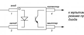
PVI: Photo Insulator for High Power Foreign Keys
Devices in this series are not relays in the proper sense of the word. That is, they are not able to commute large energy flows with the help of small ones. They only provide galvanic isolation of the input from the output, hence their name - photoelectric insulator (Fig. 5).
Rice. 5.
Why is such a “underreliance” necessary? The fact is that the PVI series devices produce, upon receiving an input signal, an electrically isolated DC voltage, which is sufficient to directly control the gates of high-power MOSFETs and IGBTs. In fact, this is an opto-relay, but without an output switch, for which the developer can use a separate transistor suitable for its power.
PVIs are ideal for applications requiring high current and/or high voltage switching with optical isolation between control circuitry and high power load circuits.
In addition, the PVI1050N
contains two simultaneously controlled outputs, which makes it possible to connect them in series or in parallel to provide a higher control current (MOC) or a higher control voltage (IGT). Thus, in fact, you can get an output signal of 10 V/5 μA when connected in series and 5 V/10 μA when connected in parallel.
The two outputs of the PVI1050N can be used separately, provided that the potential difference between the outputs does not exceed 1200 VDC. The input-output isolation is 2500 VDC.
Devices of this series are produced in 8-pin DIP packages and are used in organizing the control of powerful loads, voltage converters, etc.
We accelerate the optocoupler to hundreds
If you search the Internet for connection diagrams for optocouplers, you will find that in the vast majority of cases it is suggested to simply add a resistor. This is the simplest scheme, but it is also the slowest. When the reaction speed is not satisfactory, it is proposed to install a faster optocoupler, but, firstly, fast optocouplers are expensive, and secondly, why not accelerate the fast optocoupler to an even higher speed?
So, what is the main problem of signal transmission through an optocoupler? Typically, an optocoupler has a bipolar transistor at the output, and all bipolar transistors suffer from the problem of junction capacitance. The main problem is created by the capacitance between the collector and the base; during transient processes, it is this that prevents the transistor from quickly opening and closing. This phenomenon is called the Miller effect. Back in the days of tube receivers, they figured out how to deal with it. The main idea is that the voltage between the base and collector does not change, in this case there is no need to waste time recharging the stray capacitance.
For example, let's compare how an optocoupler behaves when turned on normally and when turned on with a constant voltage. In the first case, the capacity charges so slowly that the output signal hangs somewhere near the middle.
And now a model inclusion, which should show the maximum achievable reaction time.
This signal (red graph) looks much nicer, the edges have decreased to 0.1 µs. In the original they were somewhere around 2-3 μs, that is, an acceleration of about 20-30 times. Now the question arises, how to use this in practice, to remove the signal from the optocoupler without changing the voltage. And the first method is cascode switching (green graph).
It’s already quite good, from 100 kBit/s we have accelerated to 1 Mbit/s, but it’s still not ideal. If you add another resistor, you can build a differential amplifier.
A little bit of Tietze and Schenk, and please, the graphs practically coincided, 3 μs turned into 100 ns.
Hurray, everything works, shall we leave? No, we need more gold, so let's move on to the second part. Now we were struggling with the output capacitance, but there is also an input capacitance, and for it there are also standard circuit design methods. Why not, for example, include a capacitor at the input so that it charges the LED capacitance faster.
As you can see, this turned out to be a silver bullet for the growing front. Now we need to accelerate the falling front, and this is where the problem arises. After all, we have a unipolar power supply, and to discharge the LED we need a negative voltage. Therefore, the next step will be a level shift circuit (I don’t know if there is a generally accepted name here). We install a comparator at the output that compares the current through the optocoupler. It can be assembled from a pair of current mirrors; a similar input stage is commonly installed in op-amps and comparators.
Pairs of transistors are sold in one package, so it should be quite compact. The second silver bullet is ready, but you can see that the falling front is a little behind. And finally we came to gold: instead of a homemade comparator, we installed an industrial one. Here they are, 10 ns fronts.
You can raise the input frequency to 100 MHz and see what happens in the end.
In principle, not bad, it can be used in production, although another problem arises here - such comparators are expensive.
PS: I had a hard time selecting the values in the last circuit, so don’t expect it to work at the stated frequency.
The circuits were modeled in LTspice.
Application of optocouplers
Today, optocouplers are very well studied and widely used in various fields of activity. A special place for the use of optocouplers is in circuits for the logical coordination of various blocks that contain elements with actuators.
As already mentioned, previously optocouplers are used for galvanic isolation in circuits with excellent blocks, pulse conversion and modulation for device control, monitoring and control, signaling and protection of electrical equipment and processes (counters, switches, relays, electrical measuring devices).
Application
There are many areas in which the use of optocouplers is necessary. This breadth of application is due to the fact that they are elements that have many different properties and each of their qualities has a separate area of application.
- Fixation of mechanical impact (devices equipped with an open-type optical channel are used, which can be blocked (exert a mechanical impact), which means the device itself can be used as a sensor):
- Presence detectors (detection of the presence/absence of paper sheets in the printer);
- End (start) point detectors;
- Counters;
- Discrete speedometers.
- Galvanic isolation (the use of optocouplers makes it possible to transmit a signal not related to voltage; they also provide contactless control and protection), which can be provided by:
- Optocoupler (in most cases used as an information transmitter);
- Optorelay (mostly suitable for controlling signal and power circuits).
Usage
Optocouplers have several applications that take advantage of their different properties:
Mechanical impact
Optocouplers with an open optical channel accessible to mechanical action (overlap) are used as sensors in various presence detectors (for example, a paper detector in a printer), end (or start) sensors, counters and discrete speedometers based on them (for example, coordinate counters in a mechanical machine). mice, hydrometers).
Galvanic isolation
Optocouplers are used for galvanic isolation of circuits - signal transmission without voltage transmission, for contactless control and protection. Some standard electrical interfaces, e.g.
Non-electric transmission
The following devices are built on the optocoupler principle:
- wireless remote controls and optical input devices
- wireless (atmospheric-optical) and fiber-optic devices for transmitting analog and digital signals
Also used in non-destructive testing as emergency sensors. GaP diodes begin to emit light when exposed to radiation, and the photodetector detects a drop in its glow and reports an alarm.
Advantages and disadvantages of optoelectronic pairs
The advantages of optoelectronic pairs include almost perfect galvanic isolation, immunity of the optical communication channel to the effects of electromagnetic interference, compatibility of input and output signal parameters with integrated circuits, and wide functionality.
Disadvantages of optoelectronic pairs - low efficiency of signal energy conversion, high power consumption, temperature dependence of parameters, relatively small operating temperature range, short service life, design imperfections, etc. are temporary.
Parameters and features of the device
Based on the exact design of the device, its electrical strength can be determined. This term refers to the value of the voltage that occurs between the input and output circuits. Thus, manufacturers of optocouplers that provide galvanic isolation demonstrate a number of models with different housings:
1. DIP;2. SOP;3. SSOP;4. Miniflat-lead.
Depending on the type of housing, the optocoupler generates one or another insulation voltage. To create conditions in which the voltage level sufficient to cause insulation breakdown was high enough, the optocoupler should be designed so that the following parts are located sufficiently far from each other:
- Light diode and optical recorder;
- Inner and outer side of the case.
In some cases, you can find optocouplers of a specialized group, manufactured in accordance with international safety standards. The level of electrical strength of these models is an order of magnitude higher. Another significant parameter of a transistor optocoupler is called the “current transfer coefficient”. According to the value of this coefficient, the device is classified into one category or another, which is reflected in the model name.
There are no restrictions regarding the level of the lower operating frequency of optocouplers: they function well in a circuit with direct current. And the upper limit of the operating frequency of these devices involved in transmitting signals of digital origin is calculated in hundreds of megahertz. For linear-type optocouplers, this figure is limited to tens of megahertz. For the slowest designs, including an incandescent lamp, the most typical role is played by low-frequency filters operating at frequencies not reaching 10 Hz
There are two main reasons why the operation of a transistor pair is accompanied by noise effects:
- Pass-through capacitance between the light diode and the transistor base;
- Parasitic capacitance between the collector and the phototransistor base.
To overcome the first reason, you will need to install a special screen. The second is eliminated through a correctly selected operating mode.
Speed sensor with optocoupler.
Optorelay
An opto relay, otherwise known as a solid state relay, is usually used to regulate the operation of a circuit with large control currents. The role of the control element here is usually performed by two MOSFET transistors with back-to-back connections; this configuration ensures the ability to operate in alternating current conditions.
Classification of types of opto-relays
Three types of topologies are defined for opto-relays:
- Normally open. It is assumed that the control circuit will close only when the control voltage is applied to the terminals of the light diode.
- Normally closed. It is assumed that the control circuit will open only when the control voltage is applied to the terminals of the light diode.
- Switching. The third topology involves a combination of normally closed and normally open channels.
An opto-relay, like an optocoupler, has an electrical strength characteristic.
Types of opto-relays
- Standard type models;
- Models with low resistance;
- Models with low CxR;
- Models with low bias voltage;
- Models with high insulation voltage.
What it is
The design of an optocoupler implies the presence of a special light emitter (in modern devices, light diodes are used for this; previous models were equipped with small-sized incandescent lamps) and a device responsible for converting the received optical signal (photodetector). Both of these components are combined using an optical channel and a common housing.
There are several characteristics according to which optocoupler models can be divided into several groups. Depending on the degree of integration:
- elementary optocoupler - includes 2 or more elements united by a common housing;
- optocoupler integrated circuit - the design consists of one or more optocouplers and, in addition, can also be equipped with complementary elements (for example, an amplifier).
Depending on the type of optical channel:
- Open type optical channel;
- Closed optical channel.
Depending on the type of photodetector:
- Photoresistor (or simply resistor optocouplers);
- Photodiode optocouplers;
- Phototransistor (using a conventional or composite bipolar phototransistor) optocouplers;
- Photothyristor or phototriac optocouplers;
- Optocouplers operating using a photovoltaic generator;
- Solar battery.
An optocoupler (otherwise called an optocoupler) is an electronic device designed to convert electrical signals into light, transmit them through optical channels and re-convert the signal back into electrical.
The design of devices of the latter type is often supplemented with field-effect transistors, the same generator is responsible for controlling the gate. Phototriac optocouplers or those equipped with field-effect transistors may be called “optorelays” or “solid state relays”.
Open optocoupler connection diagram.
Scope of application of the device
They are used in a variety of fields:
- As elements of galvanic isolation, optocouplers are used: to connect equipment units between which there is a significant potential difference; to protect the input circuits of measuring devices from interference and interference.
- Another important area of application for optocouplers is optical, non-contact control of high-current and high-voltage circuits. Launch of powerful thyristors, triacs, control of electromechanical relay devices. Switching power supplies.
- The creation of “long” optocouplers (devices with an extended flexible fiber-optic light guide) opened up a completely new direction for the use of optocoupler products – communication over short distances.
- Various optocouplers are also used in radio engineering circuits for modulation, automatic gain control and others.
- Impact through the optical channel is used here to bring the circuit to the optimal operating mode, for contactless mode adjustment.
- The ability to change the properties of the optical channel under various external influences on it makes it possible to create a whole series of optocoupler sensors: these are sensors for humidity and gas contamination, sensors for the presence of a particular liquid in the volume, sensors for the cleanliness of the surface treatment of an object, and the speed of its movement.
- The versatility of optocouplers as elements of galvanic isolation and contactless control, the diversity and uniqueness of many other functions are the reason that the scope of optocoupler applications has become computer technology, automation, communications and radio equipment, automated control systems, measuring equipment, control and regulation systems, medical electronics, devices for visual display of information.
View of the optocoupler from different sides.
Advantages of optocouplers
- the ability to provide galvanic isolation between input and output;
- for optocouplers there are no fundamental physical or design restrictions on achieving arbitrarily high voltages and decoupling resistances and arbitrarily small throughput capacitance;
- the possibility of implementing contactless optical control of electronic objects and the resulting diversity and flexibility of design solutions for control circuits;
- unidirectional propagation of information along the optical channel, absence of feedback from the receiver to the emitter;
- wide frequency bandwidth of the optocoupler, no limitation from low frequencies;
- the possibility of transmitting both a pulse signal and a constant component via an optocoupler circuit;
- the ability to control the output signal of the optocoupler by influencing the material of the optical channel and the resulting possibility of creating a variety of sensors, as well as a variety of devices for transmitting information;
- the possibility of creating functional microelectronic devices with photodetectors, the characteristics of which, when illuminated, change according to a complex given law;
- the immunity of optical communication channels to the effects of electromagnetic fields, which makes them protected from interference and information leakage, and also eliminates mutual interference;
- physical, design and technological compatibility with other semiconductor and radio-electronic devices.
It will be interesting➡ What is a triac (triac)
Disadvantages of optocouplers
- significant power consumption due to the need for double energy conversion (electricity - light - electricity) and the low efficiency of these transitions;
- increased sensitivity of parameters and characteristics to the effects of elevated temperature and penetrating radiation;
- temporary degradation of optocoupler parameters;
- a relatively high level of self-noise, due, like the two previous disadvantages, to the peculiarities of the physics of LEDs;
- the complexity of implementing feedback caused by electrical isolation of the input and output circuits;
- design and technological imperfection associated with the use of hybrid non-planar technology, with the need to combine several individual crystals from different semiconductors located in different planes in one device.
Optocoupler structure
Device Description
The emitter - a packageless LED - is usually placed in the upper part of a metal case, and in the lower part - on a crystal holder - a crystal of a silicon photodetector, for example a photothyristor, is strengthened. The entire space between the LED and the photothyristor is filled with a hardening transparent mass. This fill is covered with a layer that reflects light rays inward, which prevents the scattering of light beyond the working area. The design of the resistor optocoupler differs little from the one described.
Here, in the upper part of the metal body there is a subminiature incandescent lamp, and in the lower part there is a photoresistor based on cadmium selenide. The photoresistor is made separately, on a thin glass-ceramic substrate. A film of semiconductor material, cadmium selenide, is sprayed onto it, and then forming electrodes made of a conductive material (for example, aluminum) are sprayed onto it. The output terminals are welded to the electrodes. A rigid connection between the lamp and the substrate is ensured by a hardened transparent mass. The holes in the housing for the optocoupler leads are filled with glass. The sealed connection between the lid and the base of the housing is ensured by welding.
The current-voltage characteristic (volt-ampere characteristic) of a thyristor optocoupler is approximately the same as that of a single thyristor. In the absence of input current (I=0 - dark characteristic), the photothyristor can only turn on at a very high value of the forward voltage applied to it (800...1000 V). Since in practice the application of such a large voltage is unacceptable, this curve has a purely theoretical meaning.
This is interesting! All about semiconductor diodes.
If a direct operating voltage is applied to the photothyristor (from 50 to 400 V, depending on the type of optocoupler), the device can only be turned on when an input current is supplied, which is now the control current. The turn-on speed of the optocoupler depends on the value of the input current. Typical switching times t=5…10 µs. The turn-off time of the optocoupler is associated with the process of resorption of minority current carriers in the junctions of the photothyristor and depends only on the value of the flowing output current. The actual value of the shutdown time is in the range of 10...50 µs.
It will be interesting➡ Marking of SMD transistors
The maximum and operating output current of a photoresistor optocoupler decreases sharply when the ambient temperature increases above 40 degrees Celsius. The output resistance of this optocoupler remains constant up to an input current of 4 mA, and with a further increase in the input current (when the brightness of the incandescent lamp begins to increase) it decreases sharply. In addition to those described above, there are optocouplers with the so-called open optical channel. Here the illuminator is an infrared LED, and the photodetector can be a photoresistor, photodiode or phototransistor.
The difference between this optocoupler is that its radiation goes out, is reflected from some external object and returns to the optocoupler, to the photodetector. In such an optocoupler, the output current can be controlled not only by the input current, but also by changing the position of the external reflecting surface. In optocouplers with an open optical channel, the optical axes of the emitter and receiver are located either parallel or at a slight angle. There are designs of similar optocouplers with a coaxial arrangement of optical axes. Such devices are called optochoppers.
Optocoupler or optocoupler.