The simplest schemes
The first circuit is a simple probe
for testing electrical circuits. Using this probe, you can determine the reliability of electrical contact, find an open circuit, and check the serviceability of resistors and semiconductor diodes and transistors.
To assemble a radio-electronic device, you can pre-make a DIY KIT kit using the link.
Diagram of a probe for testing the continuity of an electrical circuit.
Let's describe his work. When the XT probes are open, a high logical voltage level is set at the inputs of the logical element DD1 relative to the common wire. Accordingly, the output of element DD1 will be a low logical level, while the LED VD1 will not light up. If the probes are connected to each other, then the DD1 input will have a low logic level, and the output will be high. A glowing diode will indicate that the outputs are closed to each other. Thus, when the probes are connected to a working circuit, the LED will light up, and if the LED does not light up, it means there is an open circuit in the circuit.
The following circuit shown below is a logic probe
.
It is intended to determine the logical voltage level in the electrical circuits of digital devices. Logic probe circuit.
In the initial state, a high logical level is set at the inputs of logic element DD1 and output DD2, and accordingly the LED VD1 is lit. When the LEDs are connected to a circuit with a high logical level, the VD1 LED continues to light, and when a low logical level appears at the DD1 input, the VD1 LED will go out accordingly.
Further narration about the use of digital microcircuits is not possible without knowledge of the internal structure
digital TTL and CMOS microcircuits and their
transfer characteristics
.
What is an integrated circuit
An integrated circuit is a miniature electronic unit containing in a common housing transistors, diodes, resistors and other active and passive elements, the number of which can reach several tens of thousands.
One microcircuit can replace an entire unit of a radio receiver, an electronic computer (computer) and an electronic machine. The “mechanism” of a digital wristwatch, for example, is just one larger chip.
According to their functional purpose, integrated circuits are divided into two main groups: analog, or linear-pulse, and logical, or digital, microcircuits.
Analog microcircuits are intended for amplification, generation and conversion of electrical oscillations of different frequencies, for example, for receivers, amplifiers, and logical ones - for use in automation devices, in devices with digital timekeeping, in computers.
This workshop is devoted to familiarization with the device, operating principle and possible application of the simplest analog and logical integrated circuits.
Internal structure of TTL digital chips
All families of digital chips are based on basic logic elements
.
For all microcircuits of the TTL family, such an element is the 2I-NOT element
, which has the following internal structure.
Below is shown the diagram of the 2I-NOT element and its transient characteristic. The diagram of the basic TTL 2I-NOT element and its transient characteristic.
a multi-emitter transistor at the input of the element
VT1, then
an amplifier stage
on transistor VT2 and
a push-pull output stage
on transistors VT3, VT4.
Let us describe the operation of the 2I-NOT logic element. In the initial state, the input voltage does not exceed 0.5 V, and the emitter junction of transistor VT1 is open, this voltage is not enough to transfer the collector junction to the open state, the same applies to the emitter junctions of transistors VT2, VT4. Therefore, these transistors are closed, and transistor VT3 is open, by the voltage coming from R2. Diode VD3 turns out to be open and the voltage at the output of the element is approximately 3...4 V ( point A
).
When the voltage on the emitters of VT1 begins to increase, transistor VT2 begins to open, and transistor VT3 smoothly closes ( section A - B
).
A further increase in the voltage on the input transistor leads to the fact that transistor VT2 opens even more, the voltage on R3 also increases and transistor VT4 opens. As a result, the emitter junction of transistor VT4 bypasses resistor R3, and transistor VT2 opens sharply, and the voltage at the output of the element decreases. At this moment ( section B - C
) all transistors are open and in active mode.
If you continue to increase the input voltage, then transistors VT2 and VT4 will go into saturation mode ( section B - D
), and transistor VT3 will close and the output voltage value will become equal to the saturation voltage of transistor VT4, and the current will be limited by resistor R4.
Section B – C
The transient response can be used
to process analog signals
; in this mode, the transient response has high linearity and maximum power consumption.
Internal design of CMOS digital chips
Just like in the TTL family, the basic element of CMOS microcircuits is 2I-NOT
, the internal structure of which is shown below.
Diagram of the basic 2I-NOT CMOS element and its transient response.
Complementary field-effect transistors operate in this logic element
.
Transistors with a p-type channel (VT1, VT2)
are connected to the positive conductor of the power source,
and with an n-type channel (VT3, VT4)
they are connected in series.
At an input voltage of 2 V or less, transistors VT1 and VT2 are open, since the voltage in the gate-source sections (with a supply voltage of 9 V) is at least 7 V. The voltage in the same sections of transistors VT3 and VT4 is insufficient to open them, therefore at the output of the element there will be a voltage almost equal to the supply voltage, that is, about 9 V ( point A
).
As the input voltage increases, the transistors begin to open, and VT1 and VT2 begin to close. In section A - B
this process occurs relatively smoothly, and in
section B - C
it accelerates and is most linear.
At point B,
transistors VT1 and VT2 are almost completely closed, and VT3 and VT4 are open.
The output voltage in this case is small and with a further increase in the input voltage to the level of the power source, it tends to zero ( point G
).
Story
For more details, see Invention of the Integrated Circuit
On May 7, 1952, British radio engineer Geoffrey Dummer first proposed the idea of combining many standard electronic components into a monolithic semiconductor crystal. The implementation of these proposals in those years could not take place due to insufficient development of technology.
At the end of 1958 and in the first half of 1959, a breakthrough took place in the semiconductor industry. Three men, representing three private American corporations, solved three fundamental problems that were preventing the creation of integrated circuits. Jack Kilby of Texas Instruments
patented the principle of combination, created the first imperfect prototypes of ICs and brought them to mass production.
Kurt Legowiec of Sprague Electric Company
invented a method for electrically isolating components formed on a single semiconductor chip (pn junction isolation).
Robert Noyce of Fairchild Semiconductor
invented a method for electrically interconnecting IC components (aluminum metallization) and proposed an improved version of component insulation based on the latest planar technology of Jean Hoerni.
On September 27, 1960, Jay Last's group created
the first workable
semiconductor
Fairchild Semiconductor based on the ideas of Noyce and Ernie.
Texas Instruments
, which owned the patent for Kilby's invention, launched a patent war against competitors, which ended in 1966 with a settlement agreement on cross-licensing technologies.
Early logic ICs of the mentioned series were literally built from standard
components, the sizes and configurations of which were specified by the technological process.
Circuit designers who designed logic ICs of a particular family operated with the same standard diodes and transistors. In 1961-1962 Sylvania
lead developer Tom Longo broke the design paradigm by using, for the first time, different transistor configurations in a single IC depending on their functions in the circuit.
At the end of 1962, Sylvania
released the first family of transistor-transistor logic (TTL) developed by Longo - historically the first type of integrated logic that managed to gain a permanent foothold in the market.
In analog circuitry, a breakthrough of this level was made in 1964-1965 by Fairchild
Bob Widlar.
The first domestic microcircuit was created in 1961 at TRTI (Taganrog Radio Engineering Institute) under the leadership of L. N. Kolesov[2]. This event attracted the attention of the country's scientific community, and TRTI was approved as the leader in the system of the Ministry of Higher Education on the problem of creating highly reliable microelectronic equipment and automating its production. L.N. Kolesov himself was appointed Chairman of the Coordination Council on this problem.
The first hybrid thick-film integrated circuit in the USSR (series 201 “Trail”) was developed in 1963-65 at the Research Institute of Precision Technology (Angstrem), mass production since 1965. Specialists from NIEM (now the Argon Research Institute) took part in the development [3] [4].
The first semiconductor integrated circuit in the USSR was created on the basis of planar technology developed in early 1960 at NII-35 (then renamed Pulsar Research Institute) by a team that was later transferred to NIIME (Mikron). The creation of the first domestic silicon integrated circuit was concentrated on the development and production with military acceptance of the TS-100 series of integrated silicon circuits (37 elements - the equivalent of the circuit complexity of a flip-flop, an analogue of the American SN
-51 from
Texas Instruments
). Prototype samples and production samples of silicon integrated circuits for reproduction were obtained from the USA. The work was carried out at NII-35 (director Trutko) and the Fryazino Semiconductor Plant (director Kolmogorov) for a defense order for use in an autonomous altimeter for a ballistic missile guidance system. The development included six standard integrated silicon planar circuits of the TS-100 series and, with the organization of pilot production, took three years at NII-35 (from 1962 to 1965). It took another two years to develop factory production with military acceptance in Fryazin (1967)[5].
In parallel, work on the development of an integrated circuit was carried out in the central design bureau at the Voronezh Semiconductor Devices Plant (now OJSC NIIET). In 1965, during a visit to the VZPP by the Minister of Electronics Industry A.I. Shokin, the plant was instructed to carry out research work on the creation of a silicon monolithic circuit - R&D "Titan" (Ministry Order No. 92 of August 16, 1965), which was completed ahead of schedule completed by the end of the year. The topic was successfully submitted to the State Commission, and a series of 104 diode-transistor logic microcircuits became the first fixed achievement in the field of solid-state microelectronics, which was reflected in the MEP order No. 403 dated December 30, 1965[6][7].
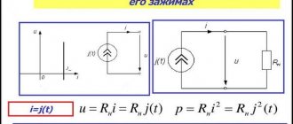
Logic element in linear mode
The use of logical elements of digital microcircuits to work with analog signals is possible only if their mode is set to linear
or close to it.
So in linear mode, a TTL element
is equivalent to an amplifier with a gain of 10 ... 15 (approximately 20 dB), and
a CMOS element
is equivalent to an amplifier with a gain of 10 ... 20 (20 ... 26 dB).
Output of a logical element into linear mode: from left to right by current, voltage, feedback.
Various methods are used to output a logical element to a linear section. One of them is based on the inclusion of resistor R at the input of the TTL element
.
This resistor will cause a current to flow through the emitter junction of the TTL element's input transistor. By changing the resistance of the external resistor, you can change the voltage at the output of the element, that is, change the position of its operating point on the transfer characteristic. For TTL elements,
the resistance of such an external resistor ranges from 1 kOhm to 3 kOhm.
However, this method is not applicable for CMOS microcircuits
, since they operate without output currents (there are leakage currents, but they are small and unstable).
The second way to bring a logic element into operating mode can be by applying the appropriate voltage to the input
, for example using
a resistive divider
.
Thus, for TTL elements
the middle of the linear section of the transfer characteristic corresponds to
an input voltage of 1.5...1.8 V
, and for
CMOS 3...6 V
(with a supply voltage of 9 V). For different logic elements this voltage is not the same, so it is selected experimentally. The values of the input resistors are chosen in such a way that the input currents of the elements do not affect the voltage removed from the resistive divider.
The third method is the most effective, for this they create negative feedback (NF)
by direct current between the input and output of the element, due to which the operating point is automatically maintained at the required portion of the transfer characteristic and does not require careful selection of external resistors.
This method is implemented for logic elements with inversion
of the input signal: NOT, NAND, NOR.
resistance in the OOS circuit
are selected based on providing the element with the required input current.
For CMOS elements
it ranges
from several kiloohms to tens of megaohms
, and for
TTL – from tens of ohms to 1 kOhm
. But the use of OOS reduces the gain of the element.
Logic amplifiers
To use logic elements as signal amplifiers, it is necessary to bring the operating point to the linear section of the transfer characteristic. The main characteristics of such amplifiers are shown in the table below.
| Series | Output circuit to linear mode | SUS, dB | Fmax, MHz | Rinput mW | Uout, V | Rin, kOhm | Rout, kOhm | R1, kOhm | R2, kOhm |
| K155 | OOC | 18 | 40 | 20 | 1,2 | 0,6 | 0,05 | 0,68 | 0,68 |
| Current | 21 | 0,8 | 1,9 | — | |||||
| K176 | OOC | 25 | 5,5 | 5 … 20 | 1,5 | 0,4 | 0,05 | 7,5 | 5,1 |
| Current | 17 | 3 … 4 | 5,0 | 3,5 | 6 | 6,2 | 4 | ||
| 561 | OOC | 25 | 1000 | 7 | 1000 | 1000 |
The circuit of the simplest amplifier based on a TTL element is shown below. Adjusting the amplifier comes down to setting the operating point of the element with the trimming resistor R1 in the middle of the linear section of the transfer characteristic.
The simplest amplifier based on a TTL element
The disadvantage of simple amplifiers is their low input impedance
, which limits their scope of application. In addition, the gain is small. This disadvantage is eliminated by using it in conjunction with transistors. The gain is increased by connecting several stages in series. In addition, the digital chip contains several identical elements, which makes it possible to create multi-channel amplifiers. An example is the diagram shown below. Main characteristics of the amplifier: gain – 50; output impedance 50 Ohm, input impedance 5 kOhm, upper limit frequency 40 MHz.
Amplifier circuit with a transistor at the input
CMOS elements can also be used for amplifiers, the circuit of one of them is shown below. A common disadvantage of CMOS amplifiers is high output impedance.
.
It can be eliminated by installing an emitter follower
on a transistor at the output of the logic element and connecting it to the OOS circuit.
Amplifier circuits based on CMOS elements.
[Contents]
Are you into electronics? We invite you to take part in beta testing of the online electrical circuit editor. sapr.asvcorp.ru Work with diagrams directly from the browser.
2.4.2 Microcircuits type LA, LI
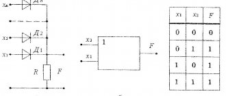
To consider the circuitry, let's make a table of functions of AND, AND-NOT elements for two inputs A and B (the simplest version).
Each variable A and B is modeled by an electronic key that can be closed or opened. If the keys are connected in series, then they work according to AND logic: current in the circuit will appear if both keys A and B are closed. If we consider the active input signals to be the closing of keys A and B and call this event logical 1, then, sequentially iterating through the state of these keys, we will compile a table of input and output data for AND and NAND elements. State table
| Logic element | Input Variables | Output function | ||
| A | B | AND | NON-AND | |
| 0 | 0 | 0 | 1 | |
| 0 | 1 | 0 | 1 | |
| 1 | 0 | 0 | 1 | |
| 1 | 1 | 1 | 0 | |
Let's consider a way to implement the logical AND-NOT operation on TTL elements. In Fig. 2.8, and a schematic diagram of a two-input AND-NOT logic element is shown.
Rice. 2.8.a. Schematic diagram of a logical element.
By supplying voltage of high B and low H levels from switches S1 and S2 to inputs A and B, we will draw up a table of the output levels of the element.
Logic element state table
| Entrance | Output Q(NAND) | Entrance | Output Q(NAND) | ||
| A | B | A | B | ||
| N | N | IN | 0 | 0 | 1 |
| N | IN | IN | 0 | 1 | 1 |
| IN | N | IN | 1 | 0 | 1 |
| IN | IN | N | 1 | 1 | 0 |
A low level voltage H appears at output Q when high voltage B is present at both inputs A and B. The graphical symbol for a two-input logic element is shown in Figure 2.8, c
Fig 2.8.c. Symbol of the element.
Among the simplest TTL ICs, AND and NAND elements predominate. Each of the LA and LI type IC packages contains from two to four logical elements, and the LA2 and LA19 microcircuits contain one NAND logical element for eight and twelve inputs, respectively.
The pinouts of microcircuits of the LA and LI types and their graphic symbols are shown in Fig. 2.9, and the main parameters are given in table. 2.3.
Figure 2.9. Symbols and pinouts of LI microcircuits Fig. 2.9. Symbols and pinouts of aircraft microcircuits
It is worth highlighting a group of microcircuits whose logical elements have open-collector outputs (LA7...LA11, LA13. LA18), (LI2, LI4, LI5). The circuit of a two-input open-collector NAND gate is shown in Fig. 2.10, a.
Rice. 2.10a. Schematic diagram of a logical element AND-NOT
To generate an output voltage drop, it is necessary to connect an external load resistor Rн to the output of such an element. Such microcircuits are used to service indicator segments, ignite incandescent lamps, and LEDs (Fig. 2.10b).
Rice. 2.10b. Connection diagram for incandescent lamps and LEDs
If necessary, a TTL element with a push-pull output can be used in circuits. For some microcircuits with an open collector output (LA11), the load can be connected to a higher voltage power source (Fig. 2.10c).
Rice. 2.10c. Diagram of connecting the load to a high-voltage source
This inclusion is necessary to ignite gas-discharge and electroluminescent indicators. Open collector outputs are used to connect relay windings.
The outputs of several elements with an open collector can be connected to a common load Rн (Fig. 2.10, d).
Rice. 2.10 Connection diagram of several elements to a common load
This connection allows you to implement a logical AND function called “wiring AND”. The circuit (Fig. 2.10. d) is used to expand the number of inputs of the logic element.
It should be remembered that push-pull TTL outputs cannot be connected in parallel, this leads to a current overload of one of the elements.
Multi-input composite logic elements with an open collector and a common load resistance Rн are the most simple to implement, but they do not allow for maximum performance. A better way to increase the number of inputs is to use a special expander microcircuit that has additional collector and emitter terminals of the VT2 phase separating cascade (Fig. 2.11). The auxiliary outputs of several such elements of the same name can be combined.
Rice. 2.11a. Schematic diagram of 2I-NOT with additional collector and emitter terminals. Rice. 2.11b. Symbol of the expander and method of connecting several microcircuits.
The K531LA16 microcircuit (main amplifier) can transmit data to a line with a resistance of 50 Ohms.
Microcircuits LA17, LA19 are NAND logic elements with three output states, i.e. they have an additional input /EO (Enable output), which gives output permission. In Fig. Figure 2.12 shows a circuit diagram of an element that has a third output state Z when the output is opened.
Rice. 2.12. Schematic diagram of a logic element with three output states.
For this purpose, an additional DDI inverter and a VD2 diode are introduced into the circuit of a standard complex TTL inverter.
If a high level voltage of 1 is applied to this input /EO from switch S1, then the output voltage of inverter DD1 will become low, i.e. the cathode of diode VD2 will be practically connected to the body. Because of this, the collector of transistor VT2 will have zero potential, i.e. transistor VT2 will be closed. Transistors VT3 and VT4 will be in cutoff mode, i.e. both are closed. Consequently, the output pin seems to “hang” in the air, the microcircuit goes into state Z with a very high output resistance. If an enabling low level - O - is applied to the EO input, then the AND-NOT logic element operates as in normal mode. Logic element state table.
| Entrance | Exit | ||
| /EO | I | /Y | |
| 0 | 0 1 | 1 0 | |
| 1 | 0 1 | Z | |
Such logic elements are designed specifically to serve the data bus conductor. If many outputs in the Z state are connected to such a conductor, they will not influence each other. Only one logical element must be an active transmitting signal; only from its output will information flow into the data bus conductor. Therefore, outputs connected together must not be active at the same time.
In order for the enable signal (low level - O) supplied to the /EO input to connect the output of only one logical element to the conductor, it is necessary to provide an additional (protective) time interval, i.e. switch the /EO inputs of different elements with a pause. The enable signals given to the outputs of different elements must not overlap.
The K531LA19 microcircuit is a 12-input AND-NOT logic element with an additional inverse input /EO. A signal will appear at its output if a low level voltage is applied to the /EO input - O. The output of the logic element will go into the open state Z if a high level voltage is applied to the /EO input. In state Z, the element consumes current Ipot.z=25 mA. The delay time for the output transition to the open state is tt.1z= 16 ns, the delay time for the output transition is tt.0z= 12 ns (from the voltage of the low output level), provided that Cn = 15 pF [1].
Threshold devices based on logic elements
Threshold devices
, called comparators, are designed to convert an analog signal into digital information.
The simplest threshold device is the Schmitt trigger, which is described in this post. In addition to generating pulses and restoring digital signals, threshold devices are used in analog-to-digital converters and pulse generators of various shapes. Diagram of a threshold device based on logical elements.
By and large, the logical element is itself a threshold device, but its transfer characteristic
not entirely linear.
To increase the linearity of the transfer characteristic of a logic element, it must be covered by positive feedback (POF)
for direct current through resistor R2.
In this case, it turns into a kind of Schmitt trigger
with the ability to regulate threshold voltages.
The width of the hysteresis loop
(the difference between the threshold voltages) depends on the ratio of the values of resistors R1 and R2.
Sensitivity also depends on these resistors. As R2 increases and R1 decreases, sensitivity increases and the width of the hysteresis loop decreases. For TTL microcircuits,
resistance R1 = 0.1 ... 2 kOhm, and R2 = 2 ... 10 kOhm.
Threshold devices based on CMOS elements are highly economical, but the disadvantage is low sensitivity. For CMOS chips,
R1 is several tens of kilo-ohms, and R2 is several hundred kilo-ohms.