Designation sizes
A selection of materials from GOST related to the size of images of conventional graphic symbols of electrical circuit elements.
All images are inserted from GOST without changes.
GOST 2.701-84 Types and types of diagrams. General requirements for implementation (fragment)
2.4.2. Conventional graphic symbols of elements are depicted in the sizes established in the standards for conventional graphic symbols. Conventional graphic symbols, the size ratios of which are given in the relevant standards on a modular grid, must be depicted on diagrams in dimensions determined vertically and horizontally by the number of steps of the modular grid M (Fig. 2a). In this case, the step of the modular grid for each circuit can be any, but the same for all elements and devices of this circuit.
Crap. 2a
Conventional graphic symbols of elements whose dimensions are not established in the specified standards must be depicted on the diagram in the dimensions in which they are made in the relevant standards for conventional graphic symbols.
The dimensions of the conventional graphic symbols, as well as the thickness of their lines, must be the same on all diagrams for a given product (installation).
Notes:
1. All sizes of graphic symbols can be changed proportionally.
2. Conventional graphic symbols of elements used as components of the symbols of other elements (devices) may be depicted smaller in comparison with other elements (for example, a resistor in a rhombic antenna, valves in a dividing panel).
GOST 2.722-68 Electrical machines (fragment)
9. Dimensions of the main elements of conventional graphic symbols, table. 3.
| Name | Designation | |
| 1. Winding | ||
| 2. Stator | ||
| 3. Rotor | ||
| 4. Brush: | on the slip ring | |
| on the collector | ||
GOST 2.721-74 Designations for general use. Table 7
| Name | Designation |
| 1. Flow of electromagnetic energy, electrical signal in one direction (for example, to the left) | |
| 2 Gas (air) flow: a) in one direction (for example, to the right) | |
| b) in both directions | |
| 3. Rectilinear movement: a) one-way | |
| b) returnable | |
| c) one-sided with a stand | |
| 4. Rotational movement: a) one-way | |
| b) one-sided with a stand | |
| 5. Regulation is linear. General designation | |
| 6. Regulation with a knob placed outside. | |
| Note to paragraphs. 3 - 6. The arrow dimensions must be within the range l = 3 ... 5, a = 15° ... 30° | |
| 7. Mechanical communication line in hydraulic and pneumatic circuits | |
| 8. Mechanical link line with step movement | |
| 9. Mechanical communication line with a time delay | |
| 10. Latch mechanism to prevent movement in both directions | |
| 11. Free release mechanism | |
| 12. Clutch: a) disengaged | |
| b) included | |
| 13. Brake | |
| 14. Deleted (Change No. 1). | |
| 15. Pusher | |
| 16. Roller | |
| 17. Roller, triggered in one direction | |
| 18. Cam | |
| 19. Ruler (slat) | |
| 20. Manual drive: a) general designation | |
| b) driven by a key | |
| c) driven by a fixed handle | |
| d) driven by a removable handle | |
| d) driven by a handwheel | |
| e) driven by pressing a button | |
| g) driven by pressing a button with limited access | |
| h) driven by a lever | |
| 21. Foot drive | |
| 22. Other drives: a) general designation | |
| b) electromagnetic | |
| c) pneumatic or hydraulic | |
| d) electric machine | |
| e) thermal (thermal engine) | |
| e) membrane | |
| g) float | |
| h) centrifugal | |
| i) using bimetal | |
| j) jet | |
| l) squib. | |
| Note to paragraphs. 1 - 20. All geometric elements of conventional graphic symbols should be made with lines of the same thickness as the connection lines. | |
Appendix 2 | |
| Name | Designation |
| Device, device | |
| Electrovacuum and ion device cylinder, semiconductor device housing | |
| Grounding, general designation | |
| Electrical connection to housing | |
| Equipotentiality | |
| A group of electrical communication lines that have a common functional purpose, carried by a multi-core cable, for example a seven-core cable | |
| Coaxial cable | |
| solid | |
| Permanent magnet | |
GOST 2.728-74 Resistors, capacitors (fragment)
7. The dimensions of the conventional graphic symbols are given in table. 6. All geometric elements of conventional graphic symbols should be made with lines of the same thickness as the electrical communication lines.
Table 6
| Name | Designation |
| 1. Constant resistor | |
| 2. A constant resistor with additional taps: a) one | |
| b) with two | |
| 3. Variable resistor | |
| 4. Variable resistor with two moving contacts | |
| 5. Trimmer resistor | |
| 6. Functional potentiometer | |
| 7. Functional ring closed potentiometer: a) single-winding | |
| b) multi-winding, for example, two-winding | |
| 8. Functional ring closed potentiometer with isolated section | |
| 9. Fixed capacitor | |
| 10. Electrolytic capacitor | |
| 11. Reference capacitor | |
| 12. Variable capacitor | |
| 13. Pass-through capacitor |
GOST 2.730-73 Semiconductor devices (fragment)
APPENDIX 2 Reference Dimensions (in a modular grid) of the main graphic symbols
| Name | Designation |
| 1 Diode 2. Thyristor diode | |
| 3. Triode thyristor | |
| 4. Transistor 5. Field effect transistor | |
| 6. Field effect transistor with insulated gate |
GOST 2.732-68 LIGHT SOURCES (fragment)
4. Dimensions of the conventional graphic designation of an incandescent lamp
GOST 2.747-68 Dimensions of graphic symbols (fragment)
2. The dimensions of the graphic symbols are given in the table.
| Name | Designation |
| 1, 2. (Excluded, Amendment No. 1) | |
| 3. According to GOST 2.755-87 | |
| 5. Heating element | |
| 6?9. (Excluded, Amendment No. 1). | |
| 10. Measuring device | |
| 11. Spark gap | |
| 12. Fuse | |
| 13. According to GOST 2.756-87 | |
| 14. Contact between telephone jack and telephone key without fixation | |
| 15. Telephone jack contact with fixation | |
| 16. According to GOST 2.756?87 | |
| 17. Telephone socket | |
| pp. 18?21 according to GOST 2.755-87 | |
| pp. 22?23 according to GOST 2.756-76 | |
| pp. 24?25 according to GOST 2.728-74 | |
| 26. (Deleted, Amendment No. 1). | |
| 27. Transformer winding | |
| 28-32 (Excluded, Amendment No. 1). | |
| Pp 33, 34 according to GOST 2 730-73 | |
| 35-40 (Excluded. Change No. 1). | |
| 41. Quantum device | |
| 42. (Deleted, Amendment No. 1). | |
| 43. Counterweight | |
| 44. Telephone set. General designation | |
| 45. Telephone and fax switchboard. General designation | |
| 46. Telephone | |
| 47. Microphone | |
| 48. Loudspeaker (reproducer) | |
| 49. Acoustic head | |
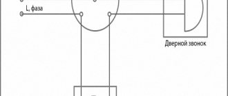
| 50. Electric bell | |
| 51. (Deleted, Amendment No. 1). | |
| 52. Electric igniter (squib) | |
| 53-55. (Excluded, Amendment No. 1). |
GOST 2.755-87 SWITCHING AND CONTACT CONNECTIONS DEVICES (fragment)
The dimensions (in the modular grid) of the main graphic symbols are given in Table 10. Table 10
| Name | Designation |
| 1. Switching device contact 1) normally open | |
| 2) opening | |
| 3) switching | |
| 2. Impulse contact when triggered and returned | |
| 3. A two-pole, six-position switch, in which the third contact of the upper pole operates earlier, and the fifth contact? later than the corresponding lower pole contacts | |
| 4. Finder with two movements with return to the starting position and multiple connection of contact fields with several finders, for example two |
GOST 2.756-76 RECEIVING PART OF ELECTROMECHANICAL DEVICES (fragment)
table 2
| Name | Designation |
| 1. Electro-mechanical device coil | |
| 2. Coil of an electro-mechanical device with one winding | |
| 3. Coil of an electromechanical device with two opposing windings | |
| 4. Coil of an electro-mechanical device with one tap | |
| 5. Electro-mechanical device reel: with one additional graphic field | |
| with two additional graphic fields | |
| 6. Sensing part of the electrothermal relay |
GOST 2.767-89 PROTECTION RELAY (fragment)
Dimensions (in a modular grid) of the main graphic symbols Table 4
| Name | Designation |
| Protection relay |
GOST 2.768?90 ELECTROCHEMICAL, ELECTROTHERMAL AND THERMAL SOURCES (fragment)
RATIO OF THE SIZES OF THE MAIN GRAPHIC SYMBOLS
| Name | Designation |
| 1. Galvanic cell | |
| 2. Thermocouple (thermocouple) | |
| 3. Non-contact heating of thermoelectric converter | |
| 4. Thermoelectric generator with heat source using combustion |
Additionally, I recommend reading the article: Dimensions of symbols in electrical circuits.
Methodical manual "Integrated circuits" educational and methodological manual on the topic
INTEGRATED CIRCUITS
Fundamentals of Microelectronics
1) Classification and UGO of integrated circuits (ICs).
2) Elements and components of hybrid ICs (GIS).
3) Elements and components of semiconductor ICs.
- Classification and UGO of integrated circuits.
IC is a microelectronic device that performs the functions of an entire electrical circuit and is designed as a single whole.
ICs are classified according to the following criteria:
- According to manufacturing technology:
Film ICs are ICs in which all elements are made in the form of thin films deposited on a dielectric base, i.e., substrate.
Hybrid (GIS) are ICs in which passive elements are made using thin-film technology, and active elements are made as separate, hinged, unframed ones.
Semiconductor ICs are microcircuits in which all elements are “grown” in a semiconductor crystal.
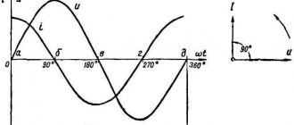
- 2. According to the method of converting and processing information, there are two types of ICs:
Analog ICs – with continuous information processing (see the process depicted in Figure 145);
Digital ICs – with discrete information processing (see Figure 146).
Rice. 57 Fig. 58
- By degree of integration: K = logN
N is the number of elements in one microcircuit package.
IC designation system
1-series IC. ICs developed on the basis of unified circuit solutions and implemented using the same technology are combined into one series. The first digit of the series is the technological sign of the IC:
1, 5, 7, 8 – semiconductor ICs; 2, 4, 6, 8 – hybrid ICs;
3 – all others.
2 – group of ICs by functional purpose: U – amplifiers
G – generators
A – signal conditioners
E – secondary power supplies (SPS) X – multifunctional circuits
L – logic circuits T – flip-flops
I - digital device circuits
B – circuits of computing devices and micro-computers – memory elements
3 – subgroup, clarifying the functional characteristic. In it, designations can be written as follows: UN, UV, UN, UT, UD. UN, for example, means “low-frequency amplifier”.
4 – type of IC according to its electrical parameters (for analog ICs) or further clarification of functions (for digital ICs).
K155LA3 – 4 elements 2I-NOT. KR, KM - a type of body, what it is made of.
One of the main elements of GIS is a substrate made of glass-ceramic material. The shape is always rectangular. The substrate is subject to high requirements in terms of surface finish, chemical resistance and electrical strength.
Contact pads and connecting conductors.
Contact pads are designed to ensure electrical contact between film elements and connecting conductors, as well as between film and hanging elements.
Rice. 59
Contact pads are most often made of aluminum, then copper, less often silver, and gold. To improve adhesion (sticking) between the conductor (contact pad) and the substrate, they are sprayed onto a nickel sublayer.
Film resistors have a rectangular shape (see Figures 60, 61).
Rice. 60 Fig. 61
If it is necessary to obtain a larger resistance value, they can be manufactured in the form of a meander. The materials used for the manufacture of resistors are nickel, nichrome, and cermets.
Film capacitors are a three-layer film structure, between which a dielectric film is applied. Aluminum, copper, and less commonly silver and gold are used for linings. Silicon oxide (SiO2;SiO), germanium monoxide (GeO), tantalum oxide (Ta2O5) is applied as a dielectric. It is not recommended, but it is allowed to spray multilayer capacitors to obtain large capacities. Film inductors are very rarely used (see Figure 62).
Rice. 62
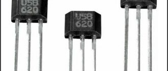
Attachment elements—diodes and transistors—can have flexible or rigid leads. The use of hinged elements with rigid leads complicates the design process of integrated circuits. But hard pins allow you to automate the assembly process.
3) Elements and components of semiconductor ICs. The basis of a semiconductor IC is a silicon substrate, usually of p-type conductivity. The manufacturing of semiconductor ICs is based on diffusion-planar or epitaxy-planar technology. Both of these methods involve the creation inside the semiconductor (i.e., in the substrate) of islands with alternating layers of p- and n-type conductivity (see Figs. 63, 64).
Rice. 63 Fig. 64
Main settings
Official publication
GOST P 55893—2013
Preface
1 DEVELOPED by the Open Joint Stock Company “Russian Research Institute “Electronstandart” (JSC “RNII “Electronstandart”)
2 INTRODUCED by the Technical Committee for Standardization TC 303 “Electronic products, materials and equipment”
3 APPROVED AND ENTERED INTO EFFECT by Order of the Federal Agency for Technical Regulation and Metrology dated December 9, 2013 No. 2199-st
4 INTRODUCED FOR THE FIRST TIME
The rules for applying this standard are established in GOST R 1.0-2012 (section 8). Information about changes to this standard is published in the annual (as of January 1 of the current year) information index “National Standards”, and the official text of changes and amendments is published in the monthly information index “National Standards”. In case of revision (replacement) or cancellation of this standard, the corresponding notice will be published in the next issue of the information index “National Standards”. Relevant information, notices and texts are also posted in the public information system - on the official website of the Federal Agency for Technical Regulation and Metrology on the Internet (gost.ru)
© Standardinform. 2014
This standard cannot be fully or partially reproduced, replicated or distributed as an official publication without permission from the Federal Agency for Technical Regulation and Metrology
GOST P 55893—2013
NATIONAL STANDARD OF THE RUSSIAN FEDERATION
Integrated circuits
Main settings
Integrated microcircuits Basic parameters
Date of introduction - 2015—01—01
1 area of use
This standard establishes the basic parameters of integrated circuits, multi-chip modules and microassemblies (hereinafter referred to as microcircuits).
Functional subgroups and types of microcircuits for which the main parameters are set are given in Appendix A.
This standard is used to select parameters when developing technical specifications for research and development work, as well as when developing technical specifications for microcircuits.
Note - This standard uses terms according to GOST 17021, GOST 26975 and GOST
19480.
2 Normative references
This standard uses references to the following standards:
GOST 17021-88 Integrated circuits. Terms and Definitions
GOST 19480-89 Integrated circuits. Terms, definitions and letter designations of electrical parameters
GOST 26975-86 Microassemblies. Terms and Definitions
Note - When using this standard, it is advisable to check the validity of the reference standards in the public information system - on the official website of the Federal Agency for Technical Regulation and Metrology on the Internet or using the annual information index "National Standards", which was published as of January 1 of the current year, and according to the releases of the monthly information index “National Standards” for the current year. If the reference standard to which an undated reference is given is replaced, then it is recommended to use the current version of this standard, taking into account all changes made to this version. If the reference standard is replaced. to which a dated reference is given, it is recommended that the version of this standard with the year of approval (adoption) indicated above be used. If, after the approval of this standard, a change is made to the reference standard to which a dated reference is given, affecting the provision to which the reference is given, then this provision is recommended to be applied without taking into account this change. If the reference standard is canceled without replacement, then the provision in which the reference is made it is recommended to be used in the part not affecting this link
Photosensitive charge coupled devices:
TL - linear; CM - matrix; CPU - others.
The fourth element is a number indicating the serial number of the development of the microcircuit in the series.
Additional symbols (from A to Z) can also be entered into the designation, defining tolerances for the variation in parameters of microcircuits, etc. The first element of the designation may be preceded by the following letters: A - plastic case of the fourth type; E - for export (lead pitch 2.54 and 1.27 mm); P - plastic housing of the second type; K - for equipment of wide application; M - ceramic, metal- or glass-ceramic body of the second type; E - metal-polymer housing of the second type; I - glass-ceramic body of the fourth type N - crystal carrier.
Computing devices:
VM - microprocessors; BE - microcomputer;
VU - microprogram control devices; VR - functional expanders; VT - memory management devices; VI - timing devices; VZh - specialized devices; ВХ - microcalculators; VF - functional information converters; VK - combined devices; BB - input-output control devices; VG - controllers; VN - interrupt control devices; VP - others.
BC - microprocessor sections; VA - devices for interfacing with the highway; VB - synchronization devices;